PAC1931/2/3/4
Single/Multi-Channel DC Power/Energy Monitor
with Accumulator
Features
Applications
• High-Side Current Monitor with One, Two, Three
or Four Channels
- 100 mV full-scale range for current sense
voltage,16-bit resolution
- Selectable bidirectional current sense
capability, -100 mV to +100 mV range, 16-bit
two’s complement (signed) data format
- External sense resistor sets full scale current
range
- Very low input current simplifies routing
• Wide Bus Voltage Range for Voltage Monitor
- 0V to 32V input common-mode voltage
- 16-bit resolution for voltage measurements;
14 bits are used for power calculations
• Real Time Auto-Calibration of Offset and Gain
Errors for Voltage and Current, No User
Adjustment Required
• 1% Power Measurement Accuracy over a Wide
Dynamic Range
• On-Chip Accumulation of 28-bit Power Results for
Energy Measurement
- 48-bit power accumulator register for
recording accumulated power data
- 24-bit Accumulator Count
- User programmable sampling rates of 8, 64,
256 and 1024 samples per second
- 17 minutes of power data accumulation
minimum at 1024 S/s
- Over 36 hours of power data accumulation
minimum at 8 S/s
• 2.7V to 5.5V Supply Operation
- Separate VDD I/O pin for digital I/O
- 1.62-5.5V capable SMBus and digital I/O
- SMBus 3.0 and I2C Fast Mode Plus (1 Mb/S)
• SMBus Address – 16 Options, set with Resistor
• No Input Filters Required
• ALERT Features that can be Enabled:
- ALERT on accumulator overflow
- ALERT on Conversion Complete
• 4 × 4 × 0.5 mm UQFN Package
• 2.225 × 2.17 mm WLCSP Package
•
•
•
•
•
•
•
•
•
•
2017-2019 Microchip Technology Inc.
Embedded Computing
Networking
FPGA Systems
Automotive
Low Voltage/High Power – AI, GPU
Industrial
Linux® Applications
Notebook and Tablet Computing
Cloud, Linux and Server Computing
Optical Networking Modules
Computing Platform Support
• Windows® 10 Driver
• Linux Driver
• Python™ Script
Description
The PAC1931/2/3/4 are one, two, three and
four-channel power and energy monitoring devices. A
high-voltage multiplexer sequentially connects the
inputs to a bus voltage monitor and current sense
amplifier that feed high-resolution ADCs. Digital
circuitry performs power calculations and energy
accumulation.
This enables energy monitoring with integration
periods from 1 ms up to 36 hours or longer. Bus
voltage, sense resistor voltage and accumulated
proportional power are stored in registers for retrieval
by the system master or Embedded Controller.
The sampling rate and energy integration period can be
controlled over SMBus or I2C. Active channel selection,
one-shot measurements and other controls are also
configurable by SMBus or I2C.
The PAC1931/2/3/4 device family uses real time
calibration to minimize offset and gain errors. No input
filters are required for this device.
DS20005850E-page 1
�PAC1931/2/3/4
Package Types
PAC1931/2/3/4 – Top View
2.225 × 2.17 mm WLCSP
SLOW/ALERT
VDD
13 SENSE2+
14 SENSE2-
VDD I/O
15
16 PWRDN
PAC1932/3/4 – Top View
4 × 4 × 0.5 mm UQFN*
1
2
12
SENSE1-
11
SENSE1+
9
SENSE4-
8
4
SENSE3+
SM_CLK
7
SENSE4+
SENSE3-
10
6
3
ADDRSEL
GND
5
2
3
4
SENSE2+
SENSE1-
SENSE1+
VDD
SENSE2-
VDD I/O
PWRDN
GND
SENSE3-
ADDRSEL
SLOW/ALERT
SM_CLK
SENSE3+
SENSE4-
SENSE4+
SM_DATA
A
B
Exposed pad
SM_DATA
1
C
D
*Includes Exposed Thermal Pad; see Table 3-1.
Device Block Diagram
VDD
SENSE 1+
VBUS1
SENSE 1-
Sen se1+
Sen se1-
SENSE 2+
VBUS2
VBUS3
SENSE 3-
Differen tia l
VSENS E
Amplifier
VBUS
Registe rs
16-bit
ADC
16-bit
ADC
Calculation
and
Calibra tion
VDD I/O
VSENS E
Registe rs
2
SENSE 3+
VBUS
Buffer/
Divi der
VPOWE R
Registe rs
Accumlato r
Sen se3+
Sen se3-
I C/SMBus
SENSE 2-
Sen se2+
Sen se2-
GND
Accumulator
Registe rs
SM_CLK
SM_DATA
SLO W/ALE RT
SENSE 4+
VBUS4
SENSE 4-
Sen se4+
Sen se4-
ADC/MUX Clocking &
Control
High
Voltage
MUX
Note:
Control
Registe rs
PWRDN
Resistor
Decoder
ADDRS EL
For PAC1931, channels 2, 3 and 4 are inactive.
For PAC1932, channels 3 and 4 are inactive.
For PAC1933, channel 4 is inactive.
DS20005850E-page 2
2017-2019 Microchip Technology Inc.
�PAC1931/2/3/4
1.0
ELECTRICAL CHARACTERISTICS
1.1
Electrical Specifications
Absolute Maximum Ratings(†)
VDD pin............................................................................................................................................................-0.3 to 6.0V
Voltage on SENSE- and SENSE+ pins ............................................................................................................-0.3 to 40V
Voltage on any other pin to GND .........................................................................................................GND -0.3 to +6.0V
Voltage between Sense pins (|(SENSE+ – SENSE-)|)..........................................................................................500 mV
Input current to any pin except VDD .................................................................................................................... ±100 mA
Output short-circuit current.............................................................................................................................. Continuous
Junction to Ambient (J-A) ...................................................................................................................................+78°C/W
Operating Ambient Temperature Range ..................................................................................................... -40 to +150°C
Storage Temperature Range....................................................................................................................... -55 to +150°C
ESD Rating – all pins – HBM...................................................................................................................................4000V
ESD Rating – all pins – CDM ..................................................................................................................................2000V
† Notice: Stresses above those listed under “Absolute Maximum Ratings” may cause permanent damage to the device.
This is a stress rating only and functional operation of the device at those or any other conditions above those indicated
in the operation listings of this specification is not implied. Exposure above maximum rating conditions for extended
periods may affect device reliability.
ESD Protection Diagram
(Floating ESD rail)
SM_DATA
SM_CLK
PWRDN
SLO W/
ALE RT
ADDRS EL
VDD I/O
GND
VDD
CLAMP
CIRCUIT
SENSE1+
SENSE2+
SENSE3+
SENSE4+
SENSE1-
SENSE2-
SENSE3-
SENSE4(~40v br eakdown)
This diagram represents the ESD protection circuitry
on the PAC1934. The SENSE pins are allowed to be at
32V if VDD is at zero. The back-to-back diodes between
the Sense+ and Sense- pins have 1 kΩ resistors in
series with them.
For PAC1931, PAC1932 and PAC1933, some of the
SENSE pins are not electrically connected inside.
These unconnected pins should be grounded.
2017-2019 Microchip Technology Inc.
DS20005850E-page 3
�PAC1931/2/3/4
TABLE 1-1:
DC CHARACTERISTICS
Electrical Characteristics: Unless otherwise specified, maximum values are at TA = -40°C to +85°C,
VDD = 2.7V to 5.5V, VDD I/O= 1.62V to 5.5V, VBUS = 0V to 32V; typical values are at TA = +25°C
VDD = VDD I/O = 3.3V, VBUS = 32V, VSENSE = (SENSE+ – SENSE-) = 0V
Characteristic
Symbol
Min.
Typ.
Max.
Unit
Conditions
Power Supply
VDD Range
VDD
2.7
—
5.5
V
VDD I/O Range
VDD I/O
1.62
—
5.5
V
VDD Pin Active
Current
IDD
—
585
675
µA
1024 Samples/s
All IDD specifications are the same
for PAC1931/2/3/4
VDD Pin Active
Current
IDD SLOW
—
16
—
µA
4 channels enabled, 8 Samples/s
Minimum VDD Rise
Rate
VDD_RISE_MIN
—
0.05
—
V/ms 0 to 5V in 100 ms
Maximum VDD Rise
Rate
VDD_RISE
—
1000
—
V/ms 0 to 5V in 5 µs
VDD Sleep Current
IDD_SLEEP
—
5
—
µA
Sleep State
VDD Power-Down
Current
IDD_PWRDN
—
0.1
—
µA
Power-Down State
IDD I/O
—
—
2
µA
All States
Common-mode range for SENSE+
and SENSE- pins, referenced to
ground (negative range not tested
in production)
VDD I/O Current
Analog Input Characteristics
VBUS Voltage Range
VBUS
–0.2V
—
32
V
VSENSE Differential
Input Voltage Range
VSENSE_DIF
–100
—
100
mV
SENSE+, SENSE- Pin
Input Current
ISENSE +, ISENSE-
–7
0
7
µA
VSENSE+ = VSENSE- = 32V
(Input current is the combined
current for the two pins)
SENSE+, SENSE- Pin
Input current
ISENSE +, ISENSE-
–1
0
1
µA
VSENSE+ = 6V, VSENSE- = 5.9V
RTRACE
—
1
—
k
—
±0.2
±1
±0.9
%
%
At +25°C
typical, -40 to +85°C
—
±0.012
±0.012
±0.1
mV
mV
At +25°C
typical, -40 to +85°C
VBUS, VSENSE Input
Trace Resistance
(allowable trace
resistance without
measurement error)
VSENSE Measurement Accuracy
VSENSE Gain
Accuracy
VSENSE Offset
Accuracy, referenced
to input
VSENSE_
GAIN_ERR
VBUS_
OFFSET_ERR
VSENSE – Unidirectional Currents
VSENSE
ADC Resolution
VSENSE_RES
—
—
16
Bits
Straight Binary for unidirectional
currents
VSENSE
Full Scale Range
VSENSE_FSR
0
—
100
mV
Unidirectional currents
VSENSE LSB Step
Size
VSENSE_LSB
—
1.5
—
µV
Unidirectional currents
DS20005850E-page 4
2017-2019 Microchip Technology Inc.
�PAC1931/2/3/4
TABLE 1-1:
DC CHARACTERISTICS (CONTINUED)
Electrical Characteristics: Unless otherwise specified, maximum values are at TA = -40°C to +85°C,
VDD = 2.7V to 5.5V, VDD I/O= 1.62V to 5.5V, VBUS = 0V to 32V; typical values are at TA = +25°C
VDD = VDD I/O = 3.3V, VBUS = 32V, VSENSE = (SENSE+ – SENSE-) = 0V
Characteristic
Symbol
Min.
Typ.
Max.
Unit
Conditions
VSENSE – Bidirectional Currents
VSENSE
ADC Resolution
VSENSE_RES
—
—
16
bits
16-bit two’s complement (signed)
VSENSE
Full Scale Range
VSENSE_FSR
-100
—
100
mV
Bidirectional currents
VSENSE LSB Step
Size
VSENSE_LSB
—
3
—
µV
Bidirectional currents
VBUS_GAIN_ERR
—
±0.02
±0.2
±0.5
%
%
At +25°C
typical, -40 to +85°C
VBUS_
—
±1
±2
—
LSB
LSB
At +25°C
typical, -40 to +85°C
Straight Binary for unidirectional
currents
VBUS Measurement Accuracy
VBUS Gain Accuracy
VBUS Offset Accuracy,
referenced to input
OFFSET_ERR
VBUS – Unipolar Voltages
VBUS
ADC Resolution
VBUS_RES
—
—
16
bits
VBUS Unipolar
Full-Scale Range
VBUS_FSR
0
—
32
V
Unipolar voltage
VBUS LSB Step Size
VBUS_LSB
—
488
—
µV
FSR = 32V, 16-bit resolution
VBUS ADC Resolution
VBUS_RES
—
—
16
bits
16-bit two's complement (signed)
numbers are reported for VBUS
measurement result
VBUS Bipolar
Full-Scale Range
VBUS_FSR
–32
—
32
V
Mathematical scaling.
Physics limits the negative input
voltage to -0.2V
VBUS LSB Step Size
VBUS_LSB
—
976
—
µV
Bipolar voltages
ACC_Err
—
0.2
—
%
VSENSE = 97 mV
ACC_Err
—
0.2
—
%
VSENSE = 10 mV
Accumulator Error
ACC_Err
—
1
—
%
VSENSE = 1 mV
Accumulator Error
ACC_Err
—
3
—
%
VSENSE = 100 µV
Accumulator Error
ACC_Err
—
5
—
%
VSENSE = 50 µV
Pull-Up Voltage
Range
VPULLUP
1.62
—
5.5
V
Pull-up voltage for I2C/SMBus pins
and digital I/O pins. Set by VDD I/O.
Time to First
Communications
tINT_T
—
14.25
—
ms
tSLEEP_TO_ACTIVE
—
3
—
ms
VBUS – Bipolar Voltages
Power Accumulator Accuracy
Accumulator Error
Accumulator Error
Active Mode Timing
Transition From Sleep
State to Start of
Conversion Cycle
Digital I/O Pins (SM_CLK, SM_DATA, SLOW/ALERT, PWRDN)
Input High Voltage
VIH
VDD I/O
x 0.7
—
—
V
Input Low Voltage
VIL
—
—
VDD I/O
x 0.3
V
2017-2019 Microchip Technology Inc.
DS20005850E-page 5
�PAC1931/2/3/4
TABLE 1-1:
DC CHARACTERISTICS (CONTINUED)
Electrical Characteristics: Unless otherwise specified, maximum values are at TA = -40°C to +85°C,
VDD = 2.7V to 5.5V, VDD I/O= 1.62V to 5.5V, VBUS = 0V to 32V; typical values are at TA = +25°C
VDD = VDD I/O = 3.3V, VBUS = 32V, VSENSE = (SENSE+ – SENSE-) = 0V
Characteristic
Symbol
Min.
Typ.
Max.
Unit
Output Low Voltage
VOL
—
—
0.4
V
Leakage Current
ILEAK
–1
—
+1
µA
DS20005850E-page 6
Conditions
Sinking 8 mA for the ALERT pin
and 20 mA for the SMCLK pin
2017-2019 Microchip Technology Inc.
�PAC1931/2/3/4
TABLE 1-2:
SMBUS MODULE SPECIFICATIONS
Electrical Characteristics: Unless otherwise specified, maximum values are at TA = -40°C to +85°C,
VDD = 2.7V to 5.5V, VBUS = 0V to 32V; Typical values are at TA = +25°C, VDD = 3.3V, VBUS = 32V,
VSENSE = (SENSE+ – SENSE-) = 0V, VDD I/O = 1.62V to 5.5V
Characteristic
Sym.
Min.
Typ.
Max.
Units
Conditions
CIN
—
4
10
pF
fSMB
.010
—
1
MHz
tSP
0
—
50
ns
tBUF
0.5
—
—
µs
Per SMBus 3.0
Hold Time after
Repeated Start
Condition
tHD:STA
0.26
—
—
µs
Per SMBus 3.0
Repeated Start
Condition Setup Time
tSU:STA
0.26
—
—
µs
Per SMBus 3.0
Setup Time: Stop
tSU:STO
0.26
—
—
µs
Per SMBus 3.0
Setup Time: Start
tSU:STA
0.26
—
—
µs
Data Hold Time
tHD:DAT
0
—
—
µs
Data Setup Time
tSU:DAT
50
—
—
ns
Per SMBus 3.0 (Note)
Clock Low Period
tLOW
0.5
—
—
µs
Per SMBus 3.0
Clock High Period
tHIGH
0.26
—
50
µs
Clock/Data Fall Time
tFALL
—
—
120
ns
Not tested in production
SMBus Interface
Input Capacitance
Not tested in production
SMBus Timing
Clock Frequency
Spike Suppression
Bus Free Time Stop to
Start
Clock/Data Rise Time
Capacitive Load
SLOW Pin Pulse Width
Note:
No minimum if Time-Out is not
enabled
tRISE
—
—
120
ns
Not tested in production
CLOAD
—
—
550
pF
Per bus line,
CLOAD not tested in production
SLOWpw
—
100
—
µs
Pulses narrower than 100 µS
may not be detected
A device must internally provide a hold time of at least 300 ns for the SM_DATA signal (with respect to the
VIH(min) of the SM_CLK signal) to bridge the undefined region of the falling edge of SM_CLK.
TLOW
THIGH
THD:STA
TRISE
SMCLK
T
THD:STA HD:DAT
TSU:STO
TFALL
TSU:DA
TSU:STA
T
SMDATA
TBUF
P
FIGURE 1-1:
S
S - Start Condition
S
P - Stop Condition
P
SMBus Timing.
2017-2019 Microchip Technology Inc.
DS20005850E-page 7
�PAC1931/2/3/4
2.0
TYPICAL OPERATING CURVES
Note:
The graphs and tables provided following this note are a statistical summary based on a limited number of
samples and are provided for informational purposes only. The performance characteristics listed herein
are not tested or guaranteed. In some graphs or tables, the data presented may be outside the specified
operating range (e.g., outside specified power supply range) and therefore outside the warranted range.
Note: Unless otherwise indicated, maximum values are at TA = -40°C to +85°C, VDD = 2.7V to 5.5V, VBUS = 0V to 32V;
typical values are at TA = +25°C, VDD = 3.3V, VBUS = 3.3V, VSENSE = (SENSE+ – SENSE-) = 0V, VDD I/O = 1.62 to 5.5V.
10
25
3.3vDC 25oC
3.3vDC 0oC
15
Error (percent)
5
Error (percent)
3.3vDC -40oC
20
0
5
3.3vDC 25oC
10
3.3vDC 85oC
5
3.3vDC 125oC
0
-5
-10
-15
-10
10uV
FIGURE 2-1:
Input Voltage.
100uV
1mV
Sense Input Voltage
100mV
VSENSE Error vs. VSENSE
1uV
0
0.0125%
-0.025%
-80 -60 -40 -20
0
20 40 60
Sense Input Voltage (mV)
Error (%FullScale)
Error (%FullScale)
CM3.3v 3.3vDC 25oC
0
-0.0125%
-0.5mV
0
0.5mV
Sense Input Voltage
Ch1 3.3vDC -40oC
o
Ch1 3.3vDC 0 C
Ch1 3.3vDC 25oC
0.025%
0
CM1v 3.3vDC 25oC
CM3v 3.3vDC 25oC
CM5v 3.3vDC 25oC
-0.025%
CM16v 3.3vDC 25oC
Ch1 3.3vDC 85oC
-0.15%
0
1mV
0.05%
0
-0.1%
100mV
FIGURE 2-5:
VSENSE Error vs. VSENSE
Input Voltage Bidirectional Mode (Zoom View).
0.05%
-0.05%
10mV
0.0125%
-0.025%
-1mV
80
FIGURE 2-2:
VSENSE Error vs. VSENSE
Input Voltage Bidirectional Mode.
0.1mV
1mV
Sense Input Voltage
0.025%
Error (%FullScale)
0.0125%
10uV
FIGURE 2-4:
VSENSE Error vs. VSENSE
Input Voltage and Temperature.
CM3.3v 3.3vDC 25oC
0.025%
Error (%FullScale)
10mV
Ch1 3.3vDC 125oC
20mV
40mV
60mV
Sense Input Voltage
80mV
100mV
FIGURE 2-3:
VSENSE Error vs. VSENSE
Input Voltage vs. Temperature.
DS20005850E-page 8
-0.05%
0
CM32v 3.3vDC 25oC
20mV
40mV
60mV
Sense Input Voltage
80mV
100mV
FIGURE 2-6:
VSENSE Error vs. VSENSE
and Common Mode.
2017-2019 Microchip Technology Inc.
�PAC1931/2/3/4
Note: Unless otherwise indicated, maximum values are at TA = -40°C to +85°C, VDD = 2.7V to 5.5V, VBUS = 0V to 32V;
typical values are at TA = +25°C, VDD = 3.3V, VBUS = 3.3V, VSENSE = (SENSE+ – SENSE-) = 0V, VDD I/O = 1.62 to 5.5V.
25
25
3.3vDC 25oC
Error (percent)
Error (percent)
20
15
10
5
20
3.3vDC 0oC
15
3.3vDC 85oC
3.3vDC 25oC
3.3vDC 125oC
10
5
0
1mV
10mV
0.1V
1V
Input Voltage
FIGURE 2-7:
Voltage.
0
1mV
10V
VBUS Error vs. VBUS Input
2%
10mV
0.1V
1V
Input Voltage
10V
FIGURE 2-10:
VBUS Error vs. VBUS Input
Voltage vs. Temperature.
2%
3.3vDC 25oC
1%
Error (percent)
1%
Error (percent)
3.3vDC -40oC
0
-1%
0
3.3vDC -40oC
3.3vDC 0oC
-1%
3.3vDC 25oC
3.3vDC 85oC
-2%
10mV
100mV
1V
Input Voltage
3.3vDC 125oC
-2%
10mV
100mV
10V
FIGURE 2-8:
VBUS Error vs. VBUS Input
Voltage (Zoom View).
-0.05%
32V
0.1%
0
Error (%FullScale)
Error (%FullScale)
0
10V
FIGURE 2-11:
VBUS Error vs. VBUS Input
Voltage vs. Temperature (Zoom View).
3.3vDC 25oC
0.05%
1V
Input Voltage
-0.2%
3.3vDC -40oC
-0.4%
3.3vDC 0oC
3.3vDC 25oC
-0.6%
3.3vDC 85oC
-0.1%
3.3vDC 125oC
-0.8%
0
FIGURE 2-9:
Voltage.
5
10
15
20
Input Voltage
25
30
VBUS Error vs. VBUS Input
2017-2019 Microchip Technology Inc.
-0.5v
0v
Input Voltage
0.5v
1v
FIGURE 2-12:
VBUS Error vs. VBUS Input
Voltage vs. Temperature (Bipolar Voltage Mode).
DS20005850E-page 9
�PAC1931/2/3/4
Note: Unless otherwise indicated, maximum values are at TA = -40°C to +85°C, VDD = 2.7V to 5.5V, VBUS = 0V to 32V;
typical values are at TA = +25°C, VDD = 3.3V, VBUS = 3.3V, VSENSE = (SENSE+ – SENSE-) = 0V, VDD I/O = 1.62 to 5.5V.
3.3vDC -40oC
0
3.3vDC 0oC
DC Offset (LSB's 15b+sign)
0.2%
Error (%FullScale)
3.3vDC 25oC
0.1%
3.3vDC 85oC
3.3vDC 125oC
0
-0.1%
-0.2%
0v
5v
10v
15v
20v
Input Voltage
25v
-0.2
-0.4
-0.6
-0.8
-1
-40
30v
FIGURE 2-13:
VBUS Error vs. VBUS Input
Voltage vs. Temperature.
0
25
55
Temperature (oC)
85
125
FIGURE 2-16:
Input Offset for VBUS
Measurements vs. Temperature.
DC Offset (LSB's 15b+sign)
0
-0.2
-0.4
-0.6
-0.8
-1
-40
FIGURE 2-14:
Zero Input Histogram for
VBUS (LSBs, 8X Average Results, Total
Population 5,000 devices).
SMBUS Drive Current (IOL) mA
60
85
125
VIO=1.6v VDD=2.6v
VIO=5.5v VDD=5.5v
50
40
30
20
10
0
0
DS20005850E-page 10
25
55
Temperature (oC)
FIGURE 2-17:
Input Offset for VSENSE
Measurements vs. Temperature.
70
FIGURE 2-15:
Zero Input Histogram for
VSENSE (LSBs, 8X Average Results, Total
Population 5,000 Devices).
0
0.1
FIGURE 2-18:
vs. VOL.
0.2
0.3
0.4
0.5
SMBUS Output Voltage (VOL)
0.6
0.7
I2C/SMBus Drive Current
2017-2019 Microchip Technology Inc.
�PAC1931/2/3/4
Note: Unless otherwise indicated, maximum values are at TA = -40°C to +85°C, VDD = 2.7V to 5.5V, VBUS = 0V to 32V;
typical values are at TA = +25°C, VDD = 3.3V, VBUS = 3.3V, VSENSE = (SENSE+ – SENSE-) = 0V, VDD I/O = 1.62 to 5.5V.
1kSps mode Current (uA)
640
620
600
580
2.6v
2.7v
3.3v
5.0v
5.5v
5.6v
560
540
520
-40
0
25
55
Temperature (oC)
85
125
FIGURE 2-19:
IDD vs. Temperature and
Supply at 1024 Samples/Second.
50
40
30
2.6v
2.7v
3.3v
5.0v
5.5v
5.6v
Sleep mode Current (uA)
8Sps mode Current (uA)
60
30
20
10
-40
0
25
55
Temperature (oC)
85
0
0
25
55
Temperature (oC)
85
125
FIGURE 2-21:
IDD for VDD I/O Pin vs.
Temperature and VDD.
2017-2019 Microchip Technology Inc.
15
2.6v
2.7v
3.3v
5.0v
5.5v
5.6v
10
5
12
VDD 2.6v/VIO 1.7v
VDD 5.6v/VIO 1.7v
VDD 2.6v/VIO 5.6v
VDD 5.6v/VIO 5.6v
0.05
-40
20
IDD vs.Temperature, VDD,
0
25
55
Temperature (oC)
85
125
FIGURE 2-23:
IDD in SLEEP Mode vs.
Temperature and VDD.
PowerDown Current (uA)
VIO Current (uA)
0.1
25
0
-40
125
FIGURE 2-20:
IDD in SLOW Mode vs.
Temperature and VDD.
0.15
FIGURE 2-22:
and Sample Rate.
10
8
6
2.6v
2.7v
3.3v
5.0v
5.5v
5.6v
4
2
0
-40
0
25
55
Temperature (oC)
85
125
FIGURE 2-24:
IDD in Power Down Mode
vs. Temperature and VDD.
DS20005850E-page 11
�PAC1931/2/3/4
Note: Unless otherwise indicated, maximum values are at TA = -40°C to +85°C, VDD = 2.7V to 5.5V, VBUS = 0V to 32V;
typical values are at TA = +25°C, VDD = 3.3V, VBUS = 3.3V, VSENSE = (SENSE+ – SENSE-) = 0V, VDD I/O = 1.62 to 5.5V.
1.5
1
0.03
0v CM
1v CM
5v CM
16v CM
32v CM
Leakage Current (uA)
Average Current 1kSps (uA)
2
0.5
0
-0.5
-40
0
25
55
Temperature (oC)
85
125
FIGURE 2-25:
VSENSE Input Current –
Active Mode, 1024 Samples/Second.
0.025
0.02
0v CM
1v CM
5v CM
16v CM
32v CM
0.015
0.01
0.005
0
-40
0
25
55
Temperature (oC)
85
125
FIGURE 2-28:
VSENSE Input Leakage
Current vs. VDD and Temperature.
Leakage Current (uA)
0.1
0.09
0.08
0.07
0.06
0v
1v
5v
16v
32v
0.05
0.04
0.03
-40
0
25
55
Temperature (oC)
85
125
FIGURE 2-26:
VBUS Input Leakage Current
vs. VDD and Temperature.
FIGURE 2-29:
Clock Frequency Error
-40°C to +85°C. Total Population 200 Devices.
Average Current 1kSps (uA)
2.5
2
1.5
0v
1v
5v
16v
32v
1
0.5
0
-40
0
25
55
Temperature (oC)
85
125
FIGURE 2-27:
VBUS Input Current – Active
Mode, 1024 Samples/Second.
DS20005850E-page 12
FIGURE 2-30:
Clock Frequency Error at
30°C. Total Population 11,189 Devices.
2017-2019 Microchip Technology Inc.
�PAC1931/2/3/4
Figure 2-31 shows the equivalent circuitry for the input
channels of the PAC193X devices. ESD protection
diodes include two 40V breakdown diodes. Input
leakage current is very low (no DC bias current). The
switched capacitor sampling circuits shown as a switch
with equivalent series resistance and sampling
capacitor. The switches work at 1024 samples per
second (SPS) maximum, independent of sampling rate
(at 8 SPS, the device is sleeping in between samples).
Input impedance for each input is about 32 MΩ.
6 kΩ
VSENSE1 kΩ
6 kΩ
30 pF
1
1
1 kΩ
30 pF
29 kΩ
VSENSE+
1.2 pF
40V
1
1
40V
VSS/GND
FIGURE 2-31:
Equivalent Input Circuits for PAC193X Devices.
2017-2019 Microchip Technology Inc.
DS20005850E-page 13
�PAC1931/2/3/4
3.0
PIN DESCRIPTIONS
The descriptions of the pins are listed in Table 3-1.
TABLE 3-1:
PIN DESCRIPTIONS
QFN
WLCSP16
Symbol
1
C3
SLOW/ALERT
Digital I/O pin
Voltage range is set by VDD I/O pin. Default function is
SLOW, may be programmed to function as ALERT pin
(Open Collector when functioning as ALERT, requires pull-up
resistor to VDD I/O).
2
A4
VDD
Power for IC
Positive power supply voltage
Description
3
B4
GND
Ground pin
Ground for the IC
4
C4
SM_CLK
SMBus clock input
Clock Input pin
5
D4
SM_DATA
SMBus data I/O
Open drain requires pull-up resistor to VDD I/O
6
C2
ADDRSEL
Analog I/O pin
Address selection for the SMBus Slave address
7(1)
C1(2)
SENSE3-
32V analog pin
0-32V range, connect to load side of sense resistor
(1)
D1(2)
SENSE3+
32V analog pin
0-32V range, connect to supply side of sense resistor
9(1)
D2(2)
SENSE4-
32V analog pin
0-32V range, connect to load side of sense resistor
D3(2)
SENSE4+
32V analog pin
0-32V range, connect to supply side of sense resistor
0-32V range, connect to supply side of sense resistor
8
10
(1)
11
A3
SENSE1+
32V analog pin
12
A2
SENSE1-
32V analog pin
0-32V range, connect to load side of sense resistor
13
A1(2)
SENSE2+
32V analog pin
0-32V range, connect to supply side of sense resistor
14
B1(2)
SENSE2-
32V analog pin
0-32V range, connect to load side of sense resistor
15
B2
VDD I/O
Sets VIH
reference for digital
I/O
Digital power reference level for digital I/O
16
B3
PWRDN
Digital input pin
Voltage range is set by VDD I/O pin. Active low puts the
device in power-down state (all circuitry is powered down
including SMBus).
—
EP
17
Note 1:
2:
3.1
Pin Type
N/C
The Exposed pad is not electrically connected
For PAC1932, pins 7,8,9,10 are not connected inside and should be grounded.
For PAC1933, pins 9 and 10 are not connected inside and should be grounded.
For PAC1931, solder balls on A1, B1, C1, D1, D2, and D3 are present but the channels are disabled internally and
should be grounded. For PAC1932, solder balls on C1, D1, D2, and D3 are present but the channels are disabled
internally and should be grounded. For PAC1933, solder balls on D2 and D3 are present but the channels are disabled
internally and should be grounded.
SenseN+/SenseN– (N=1,2,3,4)
3.5
Positive Power Supply Voltage
(VDD)
These two pins form the differential input for measuring
voltage across a sense resistor in the application. The
positive input (SenseN+) also acts as the input pin for
bus voltage.
Power supply input pin for the device. 2.7-5.5V range,
bypass with 100 nF ceramic capacitor to ground near
the IC.
3.2
3.6
Ground (GND)
System ground.
3.3
SMBus Data (SM_DATA)
This is the bi-directional SMBus data pin. This pin is
open drain, and requires a pull-up resistor to VDD I/O.
3.4
SMBus Clock (SM_CLK)
Digital Power Reference Voltage
(VDD I/O)
Connect this pin to the power supply voltage for the
digital controller driving the SMBus pins and digital
input pins for the device, 1.62V-5.5V. Bypass with
100 nF ceramic capacitor to ground near the IC. This
pin does not supply power, instead it acts as the VIH
reference.
This is the SMBus clock input pin.
DS20005850E-page 14
2017-2019 Microchip Technology Inc.
�PAC1931/2/3/4
3.7
Address Selection (ADDR_SEL)
Connect a resistor from this pin to ground to select
SMBus address.
3.8
Enable Pin (PWRDN)
Power down input pin for the device, active low.
3.9
SLOW/ALERT
In default mode, if this pin is forced high, sampling rate
is forced to eight samples/second. When it is forced
low, the sampling rate is 1024 samples/second unless
a different sample rate has been programmed.This pin
may be programmed to act as the ALERT pin, in
ALERT mode the pin needs a pull-up resistor to VDD
I/O.
3.10
Exposed Thermal Pad Pin (EP)
The Exposed pad is not electrically connected. It is
recommended that you connect it to ground.
2017-2019 Microchip Technology Inc.
DS20005850E-page 15
�PAC1931/2/3/4
4.0
GENERAL DESCRIPTION
VSENSE are converted to digital results by a 16-bit ADC,
and the digital results are multiplied to give VPOWER.
The VPOWER results are accumulated on-chip, which
enables energy measurement over the accumulation
period.
The PAC1934 is a four-channel, bidirectional, high-side
current-sensing device with precision voltage
measurement capabilities, DSP for power calculation
and a power accumulator. PAC1931, PAC1932 and
PAC1933 are one, two and three-channel versions of
the PAC1934. These devices measure the voltage
developed across an external sense resistor (VSENSE)
to represent the high-side current of a battery or
voltage regulator. The PAC1931/2/3/4 also measures
the SENSE+ pin voltages (VBUS). Both VBUS and
The PAC1931/2/3/4 has an I2C/SMBus interface for
digital control and reading results. It also has digital
supply reference VDD I/O that is to be connected to the
same supply as the digital master for the I2C/SMBUS,
enabling digital I/O voltages as low as 1.62V.
A system diagram is shown in Figure 4-1.
Sense
Resistors
VSOURCE 0V – 32V
Load
VSOURCE 0V – 32V
Load
Load
VSOURCE 0V – 32V
Load
2.7V to 5.5V
SENSE4-
SENSE3-
SENSE4+
SENSE3+
SENSE2-
SENSE2+
SENSE1-
SENSE1+
VSOURCE 0V – 32V
1.62V to 5.5V
Digital Supply
VDD I/O
VDD
PAC193X
PAC1934
ADDRSEL
SM_CLK
System
Master
SM_DATA
GND
SLOW
PWRDN
Note:
VDD and VDD I/O may be connected together.
FIGURE 4-1:
DS20005850E-page 16
PAC1931/2/3/4 System Diagram.
2017-2019 Microchip Technology Inc.
�PAC1931/2/3/4
VDD
SENSE 1+
VBUS1
SENSE 1-
Sen se1+
Sen se1-
SENSE 2+
VBUS2
SENSE 3-
16-bit
ADC
Calculation
and
Calibra tion
VDD I/O
VSENS E
Registe rs
2
SENSE 3+
Differen tia l
VSENS E
Amplifier
VBUS
Registe rs
16-bit
ADC
VPOWE R
Registe rs
VBUS3
Accumlato r
Sen se3+
Sen se3-
I C/SMBus
SENSE 2-
Sen se2+
Sen se2-
VBUS
Buffer/
Divi der
GND
Accumulator
Registe rs
SM_CLK
SM_DATA
SLO W/ALE RT
SENSE 4+
VBUS4
SENSE 4-
Sen se4+
Sen se4-
ADC/MUX Clocking &
Control
High
Voltage
MUX
FIGURE 4-2:
PAC1931/2/3/4 Functional Block Diagram.
FIGURE 4-3:
Resistor.
PCB Pattern for Sense
Control
Registe rs
PWRDN
Resistor
Decoder
ADDRS EL
Figure 4-3 shows the recommended PCB pattern for
sense resistor with wide metal for the high-current path.
The drawing shows metal, solder paste openings and
resistor outline. VSOURCE connects to the +terminal of the
high-current path, and the load connects to the -terminal
of the high-current path. Sense+ and Sense- have a
Kelvin connection to the current sense resistor to ensure
that no metal with high current is included in the VSENSE
measurement path. Sense+ and Sense- are shown as a
differential pair, route them as a differential pair to the
Sense inputs at the chip. The input pins allow for a typical
VSENSE trace resistance of 1 k, which allows the routing
flexibility far away from the chip itself on the board.
2017-2019 Microchip Technology Inc.
DS20005850E-page 17
�PAC1931/2/3/4
4.1
Detailed Description
A high-voltage multiplexer connects the input pins to
the VBUS and VSENSE amplifiers. The amplifier outputs
are sampled simultaneously for each channel,
converted by 16 bit ADCs and processed for gain and
offset error correction. After each conversion, VBUS
and VSENSE are multiplied together to give VPOWER.
An internal oscillator and digital control signals control
the two ADCs and the mux. The mux sequentially
connects each channel’s amplifiers to the ADC inputs.
The PAC1931/2/3/4 measures the source-side voltage,
VBUS, and the voltage VSENSE across an external
current sense resistor, RSENSE.
4.1.1
INITIAL OPERATION AND ACTIVE
STATE
After POR and a start-up sequence, the device is in
the Active state and begins sampling the inputs
sequentially. Voltage and current are sampled for all
active channels and power is calculated and
accumulated. All active channels are sampled at 1024
samples/second by default. Sample rates of 256, 64 or
eight samples/second may be programmed over I2C
or SMBus. If the SLOW pin is asserted the sample rate
is eight samples per second. For sampling rates lower
than 1024 samples/second, the device is in Sleep
mode for a portion of the conversion cycle, which
results in lower power dissipation. If fewer than four
channels are active, power is also reduced.
To read accumulator data and reset the accumulators,
the REFRESH command is used. To read the voltage,
current, power and accumulator data without resetting
the accumulators, the REFRESH_V command is
used. Changes to the Control register (01h) are
activated by sending either REFRESH or
REFRESH_V. When a new value is written to the
Control register (01h), the new values take effect at
the end of the next round-robin sampling cycle
following the next REFRESH or REFRESH_V
command.
4.1.2
REFRESH COMMAND
The master sends the REFRESH command after
changing the Control register and/or before reading
accumulator data from the device. The master controls
the accumulation period in this manner.
The readable registers for the VBUS, VSENSE, Power,
accumulator outputs and accumulator count are
updated by the REFRESH command and the values
will be static until the next REFRESH command.
These readable registers will be stable within 1 mS
from sending the REFRESH command, and may be
read by the master at any time up until the next
REFRESH command is sent. The internal accumulator
values and accumulator count will be reset by the
REFRESH command, but the sampling of the inputs,
DS20005850E-page 18
data conversion and power integration is not
interrupted and will continue as determined by the
settings in the Control register.
Changes written to the control and configuration
registers take effect 1 mS after a REFRESH command
is sent. Any new commands written within this 1 mS
window will be ignored and NACKed to indicate that
they are ignored.
The values for VBUS and VSENSE measurement results
and Power calculation results respond to the
REFRESH command in the same fashion as the
accumulators and accumulator count. The readable
registers will be stable within 1 mS from sending the
REFRESH command and may be read by the master
at any time. The internal values continue to be
updated according to the sampling plan determined by
the settings in the Control register. The results that are
sent to the readable registers for VBUS, VSENSE and
Power are the values from the most recent complete
conversion cycle. See Register 6-1 REFRESH
Command (Address 00h).
4.1.3
REFRESH_G COMMAND
The REFRESH_G is identical in every respect to the
REFRESH command, but it is used with the I2C
General Call address (0000 000). This allows the
system to issue a REFRESH command to all of the
PAC1931/2/3/4 devices in the system with a single
command. Then the data from this REFRESH_G
command may be read device-by-device to capture a
snapshot of the system power and energy for all
devices. See Register 6-12 REFRESH_G Command
(Address 1Eh). Note that the REFRESH_G command
can also be used with a valid Slave address but in this
case only the device with this Slave address will
receive the command. In other words it has the same
properties as the REFRESH command with the
possibility of being compatible with the I2C General
Call address.
4.1.4
REFRESH_V COMMAND
If the user wants to read VSENSE and VBUS results, the
most recent Power calculation, and/or the accumulator
values and count without resetting the accumulators,
the REFRESH_V command may be sent. Sending the
REFRESH_V command and waiting 1 mS ensures that
the VSENSE, VBUS, Power, accumulator and
accumulator count values will be stable when read by
the master. The sampling of the inputs, data conversion
and power integration are not interrupted and will
continue as determined by the settings in the Control
register. The data in these readable registers will
remain stable until the next REFRESH or REFRESH_V
command. The internal accumulator values and
accumulator count are unaffected by the REFRESH_V
command.
2017-2019 Microchip Technology Inc.
�PAC1931/2/3/4
Note that the REFRESH_V command may also be
used to activate changes to the Control register, just
like the REFRESH command, except with the
REFRESH_V command changes to the Control
register will be enacted without resetting the
accumulators
or
accumulator
count.
See
Register 6-13 REFRESH_V Command (Address
1Fh).
new sample rate to take effect and for all the sample
rate related registers (like CTRL_ACT) to show their
updated values.
4.1.5
If the SLOW pin is pulled high, the device will sample
at eight samples/second. No matter what the
programmed sample rate, this new SLOW sample rate
will take effect on the next conversion cycle (if a
round-robin conversion cycle is in process when the
SLOW pin goes high, that conversion cycle will
complete before the SLOW sample rate takes effect.)
SLEEP STATE
The SLEEP state is a lower power state than the
Active state. While in this state, the device will draw a
supply current of ISLEEP from the VDD pin. The device
automatically goes to this state between conversion
cycles when sampling rates lower than 1,024
samples/second are selected, or if fewer than four
channels are active. All digital states and data are
retained in the SLEEP state. The device can also be
put in the Sleep state by setting the SLEEP bit
followed by a REFRESH or REFRESH_V command,
and sampling will resume when the SLEEP bit is
cleared followed by a REFRESH of REFRESH_V
command. The device does not go into SLEEP state
based on any other condition such as static conditions
on the SMBus pins. If SMBus Timeout is enabled, it is
supported in SLEEP mode or ACTIVE mode.
4.1.6
POWER-DOWN STATE
The Power-Down state is entered by pulling the
PWRDN pin low. In this state, all circuits on the chip
including the SMBus pins are inactive, and the device
is in a state of minimum power dissipation.
In the Power-Down state, no data is retained in the
chip (neither register configuration nor measurement
data). When the PWRDN pin is pulled high,
integration, measurement and accumulation will begin
using the default register settings, as described in
Section 4.1.1 “Initial Operation and Active State”.
The first measurement data may be requested by a
REFRESH or REFRESH_V command 20 ms after the
PWRDN pin is pulled high.
4.1.7
PROGRAMMING THE SAMPLE
RATE AND THE SLOW PIN
The default sampling rate after power-up is 1024
samples/second. Sampling rates of 256, 64 or 8
samples/second may be programmed in the
Register 6-2 CTRL Register (Address 01h). Any time
a new sample rate is programmed, it does not take
effect until a REFRESH, REFRESH_G, or
REFRESH_V command is received. When any of
these REFRESH commands are received, any
round-robin sampling cycle in progress will complete
before the new sampling rate takes effect. For
example, if the user is sampling at 8 SPS and program
a new sample rate, it may take up to 125 mS for the
2017-2019 Microchip Technology Inc.
If one of these lower sample rates is used, power
dissipation is reduced. The round-robin sampling and
conversion cycle is exactly the same, but the device
goes into the sleep state between conversion cycles.
See Section 2.0 “Typical Operating Curves”.
If the device is programmed for Single Shot mode, and
the SLOW pin is asserted, the first sampling will begin
within 125 ms after the SLOW pin is asserted.
If the device is in the Sleep state, asserting the SLOW
pin will not cause sampling to start.
Whenever the SLOW pin changes state, a limited
REFRESH or REFRESH_V command may be
executed by the chip hardware (default is REFRESH).
Like any other REFRESH command, this resets the
accumulators and accumulator count for a REFRESH
command, and updates the readable registers for
either REFRESH or REFRESH_V. These are limited
REFRESH commands because no programmed
changes to the Control or Status registers take effect
(Control and Status registers means registers 01h,
1Ch, 1Dh, and 20h-26h). The readable registers are
stable with the new values within 1 ms of the SLOW
pin transition.
The Slow register enables selection of REFRESH or
REFRESH_V on the SLOW pin transitions, which
allows this function to be disabled for either edge, and
also tracks both the state of the SLOW pin and
transitions on the SLOW pin. See Register 6-14,
SLOW (Address 20h).
This is the default functionality of the SLOW pin, but it
may be reconfigured to function as an ALERT pin (see
paragraph Section 4.4 “Alert Functionality”). If the
SLOW pin is configured to serve as an ALERT pin, the
slower sampling rate of eight samples/second is only
available by programming the Control register 01h.
DS20005850E-page 19
�PAC1931/2/3/4
4.2
Conversion Cycles
A conversion cycle for the device consists of
analog-to-digital conversion being complete for all
channels (including the real-time calibration that is part
of each conversion cycle). Immediately following the
data conversion, the power results are calculated for
that channel and the power value is added to the
accumulator. Averaged values for VSENSE and VBUS
are also updated internally as part of each conversion
cycle.
Data conversion and processing is performed for each
active channel in sequential fashion until all active
channels have been converted, completing the
conversion cycle for the device. The sequential
sampling of each channel, along with the calculation
time and any sleep time needed to set the overall
sampling rate, is referred to as a round-robin sampling
period.
4.3
4.3.1
Conversion Cycle Controls
REDUCING THE NUMBER OF
CHANNELS TO BE SAMPLED
Program Register 6-10 CHANNEL_DIS and SMBus
(Address 1Ch) to reduce the number of channels that
are active. The sample rate is unaffected, but power
dissipation is reduced very slightly if some channels
are disabled. Any or all channels may be disabled; if
all channels are disabled, the device goes into Sleep
mode. When a channel is disabled due to register
programming in the PAC1934, or due to factory
programming on the PAC1931, PAC1932 and
PAC1933, the auto-incrementing pointer will skip
these channels by default (see Section 5.5
“Auto-Incrementing Pointer”).
4.3.2
SINGLE SHOT MODE
The Control register also allows the device to operate
in Single Shot mode. In Single Shot mode, all active
channels will sample and convert once, followed by
results being calculated. The accumulator and
accumulator count operate the same as for continuous
conversion mode, accumulating each single shot
power calculation and incrementing the accumulator
count. The conversion cycle will start when the
REFRESH
command
(or
REFRESH_V
or
REFRESH_G) is sent.
4.4
Alert Functionality
The Alert functionality can serve two purposes: to
notify the system that a conversion cycle for all active
channels is complete, or to notify the system that the
accumulator or accumulator count has overflowed.
4.4.1
USING THE ALERT FUNCTION
To use the ALERT function, configure the SLOW pin to
function as ALERT using Register 6-2 CTRL Register
(Address 01h). For this configuration, the ALERT pin
must have a pull-up to VDD I/O (it will function as an
open drain output). If a pull-up resistor is attached to
the pin for Alert functionality, the device will power up
in Slow mode. Any of the four sample rates can be
programmed using Register 6-2 CTRL Register
(Address 01h).
The Alert function for Accumulator Overflow can also
be used without reconfiguring the SLOW pin, by
monitoring the OVF bit in Register 6-2 CTRL Register
(Address 01h).
4.4.2
ALERT AFTER COMPLETE
CONVERSION
Register 6-2 has an ALERT_CC bit that can be used
to enable the ALERT_CC function. If this bit is set, the
ALERT pin will go low for 5 μS after each complete
conversion cycle is complete.
4.4.3
ALERT ON ACCUMULATOR
OVERFLOW
If the ALERT function is enabled, and any of the
accumulators or the accumulator count overflow, the
ALERT pin may be used to notify the system. To
enable this trigger for the ALERT pin, bit 1 in the
Register 6-2 CTRL Register (Address 01h) must be
set. Note that the OVF bit in the Register 6-2 CTRL
Register (Address 01h) will be set when these
overflows occur.
4.4.4
CLEARING ALERT AND OVF
When the Alert function has been tripped by
accumulator or accumulator count overflow, it will
remain asserted until a REFRESH command is
received. REFRESH_G will also clear the OVF bit and
the Alert function, but REFRESH_V will not.
After the single shot measurements and calculations
are complete, the device will go into Sleep mode. A
REFRESH, REFRESH_G or REFRESH_V command
may be sent to read the data. The user needs to wait
3 ms after the REFRESH command before
commanding another Single Shot conversion by
means of sending one of the REFRESH commands.
This is because a 1 ms delay is required between
REFRESH commands, and coming out of Sleep
requires 2 ms.
DS20005850E-page 20
2017-2019 Microchip Technology Inc.
�PAC1931/2/3/4
4.5
Voltage Measurement
The VBUS voltage for each channel is measured by the
SENSE+ pin for each channel. A high-voltage
multiplexer is connected to each SENSE+ pin, and the
multiplexer sequentially connects each SENSE+ input
to an ADC for conversion. The result is stored in a
16-bit VBUS results register and the 14 MSBs are
multiplied by the VSENSE number for the VPOWER
results value. The VPOWER results are accumulated in
the accumulator.
Full-Scale Voltage (FSV) is 32V by default. The device
may be programmed for bipolar VBUS measurements.
in this bipolar mode, the mathematical range for
negative VBUS numbers is -32V, the actual range is
limited to about -200mV due to physical factors. This
bipolar capability for VBUS enables accurate offset
measurement and correction. For bipolar operation,
the 16-bit VBUS result is a two’s complement (signed)
number.
4.7
Selecting RSENSE Values
RSENSE can easily be calculated if you know the
maximum current you want to sense, as shown in
Equation 4-2.
Consider that you may need to select a value for IMax
that includes current peaks well beyond your nominal
current.
EQUATION 4-2:
CALCULATING RSENSE
FSR
Rsense = ------------IMax
Where:
FSR
=
Full Scale VSENSE voltage input
RSENSE
=
External RSENSE resistor value
IMax
=
Maximum current to measure
The measured voltage at SENSE+ can be calculated
using Equation 4-1.
Full-Scale Current (FSC) can be calculated from
Equation 4-3.
EQUATION 4-1:
EQUATION 4-3:
V Source
BUS VOLTAGE
V BUS
= 32V ----------------------------------Denominator
FULL-SCALE CURRENT
100 mV
FSC = ---------------------R SENSE
Where:
Where:
VSOURCE = The measured voltage on the
SENSE+ pin
VBUS = The value read from the VBUS
results registers
Denominator = 216 for unipolar measurements
= 215 for bipolar measurements
4.6
FSC
=
Full-scale current
RSENSE
=
External sense resistor value
The actual current through RSENSE can then be
calculated using Equation 4-4.
EQUATION 4-4:
V SENSE
I SENSE = FSC ----------------------------------Denominator
Current Measurement
The PAC1931/2/3/4 device family includes high-side
current sensing circuits. These circuits measure the
voltage (VSENSE) induced across a fixed external
current sense resistor (RSENSE) and store the voltage
as a 16-bit number in the VSENSE Results registers.
The PAC1931/2/3/4 current sensing operates with a
Full-Scale Range (FSR) of 100 mV in unidirectional
mode (default).
When sensing unidirectional currents (the default
mode), the ADC results are presented in straight binary
format. For bidirectional current sensing, the ADC
results are in two’s complement (signed) format. For
bipolar current measurements, the range is ±100 mV,
but use FSR = 100 mV in the equations that follow. For
best accuracy on current values near zero, it is
recommended to use the bidirectional current mode
and 8x average current results.
2017-2019 Microchip Technology Inc.
SENSE CURRENT
Where:
ISENSE
=
Actual bus current
FSC
=
Full-scale current value (from
Equation 4-3)
VSENSE
=
The value read from the
VSENSE results registers
Denominator
=
216 for unipolar measurements
=
215 for bipolar measurements
DS20005850E-page 21
�PAC1931/2/3/4
4.8
ADC Measurements, Offset, and
8x Averaging
The PAC1931/2/3/4 is primarily desired for energy
measurements where many power readings are
accumulated. This is inherently an averaging process.
Individual voltage and current measurements can also
benefit from averaging to reduce noise and offset.
Averaged values are internally calculated for VBUS and
VSENSE, with a rolling average of the most recent eight
values present in the VBUSn_AVG (Register 6-7) and
VSENSEn_AVG (Register 6-6) registers. The average
is updated internally after every conversion cycle. The
readable registers are updated with REFRESH,
REFRESH_V, or REFRESH_G commands like all the
other readable results registers. These averaged
results may be used for the most accurate, lowest
noise and lowest offset measurements.
The ADC channels use a special offset canceling
technique. If the user observes the unaveraged results
for near-zero values of VBUS and VSENSE, they may
observe a cyclical pattern of offset variation. The user
may think this is noise, but in fact it is due to internal
circuitry switching through different permutations of
offset cancellation circuitry. This small variation in
unaveraged offset is canceled in the 8x averaged
result. It is also canceled in the Power Accumulator
results. The overall effect is offset that is consistently
very close to zero LSB over supply and temperature
variations.
The offset canceling technique is illustrated in
Figure 4-4. It is very difficult to accurately observe, as
it is a challenge to read the data from every conversion
cycle. The effect of capturing data points at a rate that
does not correspond exactly to the internal sampling
rate of the PAC1931/2/3/4 can make these
permutations appear less periodic and deterministic
than they are inside the chip. The data conversion uses
one of the permute positions 1-4 for each input on each
conversion, cycling through all four permutations in four
conversions. When averaged the Permute Enabled
result shown below is realized, evenly distributed
around zero.
DS20005850E-page 22
FIGURE 4-4:
Illustration of the Four
Permute Combinations that the ADC Cycles
through and the Resulting Low Average Offset.
Each Bin Represents One Code.
Results from both the VBUS and VSENSE ADCs are 17b
two's complement (signed) internally. There is an
additional bit of resolution that is not accessible from the
results register. The NEG_PWR (Address 1Dh) register
determines whether the conversion results are reported
in the readable registers as unipolar or bipolar numbers.
Using bipolar numbers can give more accurate results
for very small numbers that may actually be negative for
some readings, in addition to measuring bidirectional
currents (charging/discharging) and voltages that can dip
below ground.
Averaged values are also calculated for VBUS and
VSENSE. A rolling average of the most recent eight
values is present in the VBUSn_AVG (Register 6-7)
and VSENSEn_AVG (Register 6-6) registers. These
registers require eight conversion cycles after POR
before they represent an accurate value, they are
updated after every conversion cycle. The readable
registers are updated with REFRESH, REFRESH_V
or REFRESH_G commands like all the other readable
results registers.
2017-2019 Microchip Technology Inc.
�PAC1931/2/3/4
4.9
Power and Energy
The Full-Scale Range for Power depends on the
external sense resistor used, as shown in
Equation 4-5.
EQUATION 4-5:
POWER FSR
CALCULATION
PowerFSR = 100 mV R SENSE 32V
accumulation period, T. In this equation, T must be
known from a system clock time stamp or other
accurate indicator of the total accumulation period.
EQUATION 4-8:
V accum
T
Energy = ----------------------------------- PwrFSR -------------------------Denominator
AccCount
Where:
2
= 3.2V R SENSE
Denominator
Where:
RSENSE
=
External RSENSE resistor value
100 mV
=
Full-Scale VSENSE voltage input
32V
=
Full-Scale VBUS voltage input
The device implements Power measurements by
multiplying VBUS and the VSENSE to give a result
VPOWER. VPOWER values are used to calculate
Proportional Power as shown in Equation 4-6. The
Proportional Power is the fractional portion of Power
FSR measured in one sample. Bipolar mode is where
VBUS is bipolar mode, VBUS is bidirectional mode, or
both VBUS and VSENSE are bipolar/bidirectional.
EQUATION 4-6:
ENERGY CALCULATION
=
228 (unipolar mode)
=
227 (bipolar mode)
EQUATION 4-9:
ENERGY CALCULATION
V accum
PwrFSR
Energy = ----------------------------------- -------------------------Denominator
fs
Where:
Denominator
=
228 (unipolar mode)
=
227 (bipolar mode)
Equation 4-9 shows how to calculate energy using the
accumulated power and the sampling rate, fs.
PROPORTIONAL POWER
CALCULATION
Vpower
P PROP = ----------------------------------Denominator
Where:
Denominator
=
=
228 (unipolar mode)
227 (bipolar mode)
To calculate the actual power from the Proportional
Power, multiply by the Power FSR as shown in
Equation 4-7. This Actual Power number is the power
measured in one sample.
EQUATION 4-7:
POWER CALCULATION
P actual = PowerFSR P PROP
These VPOWER results are digitally accumulated on
chip, and stored in the VACCUM registers.
The energy calculation Equations 4-8 and 4-9 use a
different denominator term depending on unipolar or
bipolar mode. Bipolar mode for energy applies when
bipolar/bidirectional mode is used for VBUS and/or
VSENSE. Equation 4-8 shows how to realize this using
the Accumulator results, Accumulator count and the
2017-2019 Microchip Technology Inc.
DS20005850E-page 23
�PAC1931/2/3/4
4.9.1
ADDITIONAL ACCUMULATOR
INFORMATION
The math for the Power calculation and accumulation
inside the chip is always done in two's complement
math, no matter what the user sets the output registers
to show. VBUS and VSENSE are 17-bit two's
complement (signed) numbers internally. VPOWER is
the product of VSENSE multiplied by the 14 MSBs of
VBUS, and this is a 31 bit two's complement result
(signed) internally. In some cases this results in a
Power result that is not identical to the product of the
VBUS results register multiplied by the VSENSE register.
However, the Power result from the Power results
register is more accurate than the product of the VBUS
register multiplied by the VSENSE register in these
cases, as explained below.
not all be full-scale numbers; this is especially true if
VBUS is not 32V. If VBUS is a lower number, the
maximum number of full-scale samples that can be
accumulated is scaled by 32V/VBUS. This limitation can
limit the accumulation period before overflow to 17
minutes at 1024 samples/second, or 36 hours at eight
samples/second, if most values are near full-scale. The
Accumulator Count limit described above will still limit
the total number of samples to 224.
If VSENSE and VBUS are both programmed to be
unsigned (unipolar) in register NEG_PWR (Address
1Dh), 16b without sign are exported to VBUS and
VSENSE results registers.
If VBUS is programmed to be signed (bipolar) in
Register 6-11 NEG_PWR (Address 1Dh), the
corresponding data is truncated to 16-bit two's
complement (signed) for the readable results register.
If VSENSE is programmed to be signed (bipolar) in
register NEG_PWR (Address 1Dh), the corresponding
results register value is truncated to 16-bit two's
complement (signed), but the power calculation uses
17-bit two's complement (signed). Therefore, a
mismatch is possible between an externally calculated
power value (VBUS times VSENSE) and the actual power
value calculated internally to the chip. The internally
calculated (and accumulated) value is more accurate
than the externally calculated value in every case.
The continuous power integration periods (also called
the energy accumulation period) can range from ~1ms
to many hours, depending on the number of samples
per second selected via SMBus. The number of
samples is limited by the size of the Accumulator Count
register to 16,777,216 (224). This count corresponds to
about 273 minutes at 1024 samples/second, or 582
hours at eight samples/second. This Accumulator
Count can overflow, and it will not reset when it
overflows.
When the accumulation registers reach their maximum
value, this is called accumulator overflow. The
accumulator outputs remain at their maximum value;
they do not roll over. The user can calculate the
worst-case time to roll over and read them at or before
that time or use the built in Alert functions to detect
rollover and read them at that time.
Worst-case accumulator overflow time can be
calculated assuming that every measurement that is
accumulated is a full-scale number. Since the power
numbers are 28 bits, and the accumulator is 48 bits, 220
samples can be accumulated before overflow if they
are all full-scale values. For most applications, they will
DS20005850E-page 24
2017-2019 Microchip Technology Inc.
�PAC1931/2/3/4
NOTES:
2017-2019 Microchip Technology Inc.
DS20005850E-page 25
�PAC1931/2/3/4
5.0
SMBUS AND I2C
COMMUNICATIONS
PROTOCOL
The PAC1931/2/3/4 communicates over a two-wire bus
with a controller using SMBus or I2C serial
communication protocol. A detailed timing diagram is
shown in Figure 1-1.
Stretching of the SMCLK signal is supported; however,
the PAC1931/2/3/4 will not stretch the clock signal.
5.1
5.1.1
I2C/SMBus Addressing and
Control Bits
SMBUS ADDRESS AND RD/WR BIT
The SMBus Address Byte consists of the 7-bit slave
address followed by a 1-bit RD / WR indicator. If this
RD / WR bit is a logic ‘0’, the SMBus master is writing
data to the slave device. If this RD / WR bit is a logic
‘1’, the SMBus master is reading data from the slave
device.
The PAC1931/2/3/4 I2C/SMBus address is determined
by a single pull-down resistor connected between
ground and the ADDRSEL pin as shown in Table 5-1.
The chip translates the resistor value into an address
on power-up, and the value is latched until another
power-up event takes place. The address cannot be
changed on the fly.
5.1.2
5.1.5
SMBUS DATA BYTES
All SMBus data bytes are sent most significant bit first
and composed of eight bits of information.
TABLE 5-1:
ADDRESS SELECT
RESISTOR
Resistor (1%)
SMBus Address
0 (Tie to GND)
499
806
1,270
2,050
3,240
5,230
8,450
13,300
21,500
34,000
54,900
88,700
140,000
226,000
Tie to VDD
0010_000(r/w)
0010_001(r/w)
0010_010(r/w)
0010_011(r/w)
0010_100(r/w)
0010_101(r/w)
0010_110(r/w)
0010_111(r/w)
0011_000(r/w)
0011_001(r/w)
0011_010(r/w)
0011_011(r/w)
0011_100(r/w)
0011_101(r/w)
0011_110(r/w)
0011_111(r/w)
SMBUS START BIT
The SMBus Start bit is defined as a transition of the
SMBus data line from a logic ‘1’ state to a logic ‘0’ state
while the SMBus Clock line is in a logic ‘1’ state.
5.1.3
SMBUS ACK AND NACK BITS
The SMBus slave will ACK (acknowledge) all data
bytes that it receives. This is done by the slave device
pulling the SMBus data line low after the eighth bit of
each byte that is transmitted.
5.1.4
SMBUS STOP BIT
The SMBus Stop bit is defined as a transition of the
SMBus data line from a logic ‘0’ state to a logic ‘1’ state
while the SMBus clock line is in a logic ‘1’ state. When
the PAC1931/2/3/4 detects an SMBus Stop bit, and it
has been communicating with the SMBus protocol, it
will reset its slave interface and prepare to receive
further communications.
DS20005850E-page 26
2017-2019 Microchip Technology Inc.
�PAC1931/2/3/4
5.2
SMBus Time-Out
The PAC1931/2/3/4 can support the SMBus Time-Out
functionality. This functionality is disabled by default,
and can be enabled by writing to the Timeout bit (see
Register 6-10 CHANNEL_DIS and SMBus (Address
1Ch).
If Time-Out is enabled and the clock is held at logic ‘0’
for tTIMEOUT = 25-43 ms, the device will time-out and
reset the SMBus interface. Communication is restored
with a start condition.
5.3
SMBus and I2C Compatibility
The PAC1931/2/3/4 is compatible with SMBus 3.0
1 MHz class and I2C Fast-mode Plus. The major
differences between SMBus and I2C devices are
highlighted here. For more information, refer to the
SMBus 3.0 and I2C specifications.
1.
2.
3.
4.
If Time-Out function is enabled, the minimum
frequency for SMBus communications is
10 kHz. If Time-Out function is disabled (default
condition), then there is no minimum frequency
for SMBus communications.
If SMBus Time-Out is enabled in Register 6-10:
CHANNEL_DIS and SMBus (Address 1Ch),the
SMBus slave protocol will reset if the clock is
held at a logic ‘0’ for tTIMEOUT. I2C does not have
a time-out, this is the default condition.
I2C devices do not support the Alert Response
Address functionality (which is optional for
SMBus).The PAC1931/2/3/4 does not support
the Alert Response Address functionality;
instead, the ALERT is a GPIO pin that may be
monitored by the master or Embedded
Controller.
I2C devices support Block Read and Block Write
differently. I2C protocol allows for unlimited
number of bytes to be sent in either direction.
The SMBus protocol for Block Read and Block
Write requires that an additional data byte
indicating number of bytes to read/write is
transmitted. PAC1931/2/3/4 devices support the
I2C protocol for Block Read by default (no byte
count information is sent). If the Byte Count bit is
set (see Register 6-10: CHANNEL_DIS and
SMBus (Address 1Ch), it will be sent as the first
data byte in response to the Block Read
command, per SMBus protocol.
2017-2019 Microchip Technology Inc.
5.4
I2C/SMBus Protocols
The PAC1931/2/3/4 supports Write Byte, Read Byte,
Block Read, Send Byte and Receive Byte as valid
protocols.
It will not respond to the Alert Response Address
protocol. It will respond to the I2C General Call
Address.
All of the protocol charts listed below use the
convention in Table 5-2.
TABLE 5-2:
PROTOCOL FORMAT
Data Sent to Device
# of bits sent
5.5
Data Sent to the Master
# of bits sent
Auto-Incrementing Pointer
The PAC1931/2/3/4 has an auto-incrementing address
pointer. The pointer has two loops for auto-incrementing,
a read loop and a write loop.
The read loop includes all of the readable registers,
including all of the configuration and Control registers,
the results registers, and the Product ID, Manufacturer
ID and Revision ID registers.
The write loop includes only the writable control and
configuration registers.
Neither loop includes the REFRESH commands.
The read loop will skip inactive channels, if some
channels have been disabled. This automatic channel
skipping feature can be disabled by setting the No Skip
bit in Register 6-10: CHANNEL_DIS and SMBus
(Address 1Ch).
If the user elects to read disabled channels, they will
return FFh and the register address will by NACKed.
See Figure 5-1 for a graphic representation.
DS20005850E-page 27
�PAC1931/2/3/4
App Read Loop
0x00 W
App Write Loop
Channels ON or
(Channels OFF and
Skip OFF)
Channels 1 & 4 OFF
and Skip ON
Channels OFF and
Skip ON
Don’t care if Channels
ON or OFF
REFRESH
REFRESH
REFRESH
REFRESH
CTRL
CTRL
CTRL
CTRL
1 byte
0x01 R/W 1 byte
0x02 R
3 bytes
ACC_COUNT
ACC_COUNT
ACC_COUNT
ACC_COUNT
0x03 R
6 bytes
VPOWER1_ACC
VPOWER1_ACC
VPOWER1_ACC
VPOWER1_ACC
0x04 R
6 bytes
VPOWER2_ACC
VPOWER2_ACC
VPOWER2_ACC
VPOWER2_ACC
0x05 R
6 bytes
VPOWER3_ACC
VPOWER3_ACC
VPOWER3_ACC
VPOWER3_ACC
0x06 R
6 bytes
VPOWER4_ACC
VPOWER4_ACC
VPOWER4_ACC
VPOWER4_ACC
0x07 R
2 bytes
VBUS1
VBUS1
VBUS1
VBUS1
0x08 R
2 bytes
VBUS2
VBUS2
VBUS2
VBUS2
0x09 R
2 bytes
VBUS3
VBUS3
VBUS3
VBUS3
0x0A R
2 bytes
VBUS4
VBUS4
VBUS4
VBUS4
0x0B R
2 bytes
VSENSE1
VSENSE1
VSENSE1
VSENSE1
0x0C R
2 bytes
VSENSE2
VSENSE2
VSENSE2
VSENSE2
0x0D R
2 bytes
VSENSE3
VSENSE3
VSENSE3
VSENSE3
0x0E R
2 bytes
VSENSE4
VSENSE4
VSENSE4
VSENSE4
0x0F R
2 bytes
VBUS1_AVG
VBUS1_AVG
VBUS1_AVG
VBUS1_AVG
0x10 R
2 bytes
VBUS2_AVG
VBUS2_AVG
VBUS2_AVG
VBUS2_AVG
0x11 R
2 bytes
VBUS3_AVG
VBUS3_AVG
VBUS3_AVG
VBUS3_AVG
0x12 R
2 bytes
VBUS4_AVG
VBUS4_AVG
VBUS4_AVG
VBUS4_AVG
0x13 R
2 bytes
VSENSE1_AVG
VSENSE1_AVG
VSENSE1_AVG
VSENSE1_AVG
0x14 R
2 bytes
VSENSE2_AVG
VSENSE2_AVG
VSENSE2_AVG
VSENSE2_AVG
0x15 R
2 bytes
VSENSE3_AVG
VSENSE3_AVG
VSENSE3_AVG
VSENSE3_AVG
0x16 R
2 bytes
VSENSE4_AVG
VSENSE4_AVG
VSENSE4_AVG
VSENSE4_AVG
0x17 R
4 bytes
VPOWER1
VPOWER1
VPOWER1
VPOWER1
0x18 R
4 bytes
VPOWER2
VPOWER2
VPOWER2
VPOWER2
0x19 R
4 bytes
VPOWER3
VPOWER3
VPOWER3
VPOWER3
0x1A R
4 bytes
VPOWER4
VPOWER4
VPOWER4
VPOWER4
CHANNEL_DIS
CHANNEL_DIS
CHANNEL_DIS
CHANNEL_DIS
0x1C R/W 1 byte
NEG_PWR
NEG_PWR
NEG_PWR
NEG_PWR
0x1E W
1 byte
REFRESH_G
REFRESH_G
REFRESH_G
REFRESH_G
0x1F W
1 byte
REFRESH_V
REFRESH_V
REFRESH_V
REFRESH_V
SLOW
SLOW
SLOW
SLOW
0x1D R/W 1 byte
0x20 R/W 1 byte
0x21 R
1 byte
CTRL_ACT
CTRL_ACT
CTRL_ACT
CTRL_ACT
0x22 R
1 byte
CHANNEL_DIS_ACT
CHANNEL_DIS_ACT
CHANNEL_DIS_ACT
CHANNEL_DIS_ACT
0x23 R
1 byte
NEG_PWR_ACT
NEG_PWR_ACT
NEG_PWR_ACT
NEG_PWR_ACT
0x24 R
1 byte
CTRL_LAT
CTRL_LAT
CTRL_LAT
CTRL_LAT
0x25 R
1 byte
CHANNEL_DIS_LAT
CHANNEL_DIS_LAT
CHANNEL_DIS_LAT
CHANNEL_DIS_LAT
0x26 R
1 byte
NEG_PWR_LAT
NEG_PWR_LAT
NEG_PWR_LAT
NEG_PWR_LAT
0xF D R
1 byte
PID
PID
PID
PID
0xF E R
1 byte
MID
MID
MID
MID
0xF F R
1 byte
REV
REV
REV
REV
FIGURE 5-1:
READ and WRITE Auto Incrementing Loops.
Figure 5-1 shows how the auto-incrementing READ
loop works with SKIP option on and off, for reading. It
also shows how the WRITE loop works with the
REFRESH,
REFRESH_V,
and
REFRESH_G
commands.
DS20005850E-page 28
2017-2019 Microchip Technology Inc.
�PAC1931/2/3/4
I2C/SMBus Commands
5.6
5.6.1
REFRESH AND REFRESH_V
REFRESH and REFRESH_V commands are sent
using the Send byte command, the Slave Address and
the desired command (00h for REFRESH or 1Fh for
REFRESH_V. See Table 5-3.
TABLE 5-3:
REFRESH AND REFRESH_V COMMANDS
START
Slave Address
WR
ACK
REFRESH or
REFRESH_V
Command
ACK
STOP
10
YYYY_YYY
0
0
00h or 1Fh
0
01
5.6.2
GENERAL CALL ADDRESS
RESPONSE
Just as the REFRESH command is sent using a Send
Byte command with the slave address, and the
REFRESH command (00h), the REFRESH_G
command is sent using Send Byte with the General
Call address (0000 000) and the REFRESH_G
command (1Eh).
When the master sends the General Call address, the
PAC1931/2/3/4 will be able to execute the REFRESH
command by means of a second version of the
REFRESH command called REFRESH_G (see
Register 6-12 REFRESH_G Command (Address
1Eh)).
TABLE 5-4:
Table 5-4 shows the response to the General Call
command for REFRESH_G.
GENERAL CALL RESPONSE
START
General Call
Address
WR
ACK
REFRESH_G
Command
ACK
STOP
10
0000_000
0
0
1Eh
0
01
5.6.3
WRITE BYTE
The Write Byte is used to write one byte of data to the
registers, as shown in Table 5-5.
TABLE 5-5:
WRITE BYTE PROTOCOL
START
Slave
Address
WR
ACK
Register
Address
ACK
Register
Data
ACK
STOP
10
YYYY_YYY
0
0
XXh
0
XXh
0
01
2017-2019 Microchip Technology Inc.
DS20005850E-page 29
�PAC1931/2/3/4
5.6.4
READ BYTE
The Read Byte protocol is used to read one byte of data
from the registers, as shown in Table 5-6.
If an invalid register address is specified, the slave will
ACK its address but NACK (not acknowledge) the
register address.
The master will NACK the data received from the slave
by holding the SMBus data line high after the eighth
data bit has been sent.
TABLE 5-6:
READ BYTE PROTOCOL
START
Slave
Address
WR
ACK
Register
Address
ACK
START
Slave Address
RD
ACK
Register Data
NACK
STOP
10
YYYY_YYY
0
0
XXh
0
10
YYYY_YYY
1
0
XXh
1
01
5.6.5
SEND BYTE
The Send Byte protocol is used to set the internal
address register pointer to the correct address location.
No data is transferred during the Send Byte protocol,
as shown in Table 5-7.
TABLE 5-7:
SEND BYTE PROTOCOL
START
Slave Address
WR
ACK
Register Address
ACK
STOP
10
YYYY_YYY
0
0
XXh
0
01
5.6.6
RECEIVE BYTE
If the master wishes to continue clocking and read the
next register, the master will ACK after the register
data, instead of sending NACK followed by STOP.
The Receive Byte protocol is used to read data from a
register when the internal register address pointer is
known to be at the right location (e.g., set via Send
Byte). This is shown in Table 5-8.
If some channels are deactivated, their data registers
will be skipped by the auto-incrementing pointer.
Alternatively, you may set bit 0 in Register 6-10
CHANNEL_DIS and SMBus (Address 1Ch) and the
pointer will not skip the addresses associated with the
inactive channels. The measurement data for these
inactive channels will read FFh.
When an ACK is received after the REGISTER DATA,
then the address pointer automatically increments.
When a NACK is received after the REGISTER DATA,
then the address pointer stays at the same position.
TABLE 5-8:
RECEIVE BYTE PROTOCOL
START
Slave Address
RD
ACK
Register Data
NACK
STOP
10
YYYY_YYY
1
0
XXh
1
01
DS20005850E-page 30
2017-2019 Microchip Technology Inc.
�PAC1931/2/3/4
5.6.7
BLOCK READ – I2C VERSION
Block Read is used to read multiple data bytes from a
register that contains more than one byte of data, or
from a group of contiguous registers, as shown in
Table 5-9. The PAC1931/2/3/4 supports I2C Block
Read by default, but the SMBus format can also be
supported (see Table 5-10).
If an invalid register address is specified, the slave will
ACK its address but NACK the register address.
The master will NACK the data received from the slave
by holding the SMBus data line high after the 8th data
bit has been sent.
BLOCK READ PROTOCOL I2C VERSION (DEFAULT)
TABLE 5-9:
START
Slave Address
WR
ACK
Register
Address
ACK
START
Slave Address
RD
ACK
Register
Data
1 0
YYYY_YYY
0
0
XXh
0
1 0
YYYY_YYY
1
0
XXh
ACK
Register Data
ACK
Register
Data
ACK
Register
Data
ACK
Register
Data
NACK
STOP
0
XXh
0
XXh
0
XXh
0
XXh
1
01
5.6.8
BLOCK READ – SMBUS VERSION
PAC1931/2/3/4 can also support the SMBus version of
Block Read. If the Byte Count bit is set, Block Read will
result in the device sending the Byte Count data before
the first data byte. This protocol is shown in Table 5-10.
Also see Section 4.3 “Conversion Cycle Controls”
above and Register 6-10 CHANNEL_DIS and SMBus
(Address 1Ch).
TABLE 5-10:
BLOCK READ PROTOCOL SMBUS VERSION (MUST SET BYTE COUNT BIT)
START
Slave Address
WR
ACK
Register
Address
ACK
START
Slave Address
RD
ACK
Byte Count
1 0
YYYY_YYY
0
0
XXh
0
1 0
YYYY_YYY
1
0
XXh = N
ACK
Register Data
ACK
Register
Data
ACK
Register
Data
ACK
Register
Data
NACK
STOP
0
XXh
0
XXh
0
XXh
0
XXh
1
01
2017-2019 Microchip Technology Inc.
DS20005850E-page 31
�PAC1931/2/3/4
6.0
REGISTERS IN HEXADECIMAL
ORDER
The registers shown in Table 6-1 are accessible
through the SMBus. In the individual register tables that
follow, an entry of ‘—’ indicates that the bit is not used
and will always read ‘0’.
Data represented by the data registers are ensured to
be synchronized and stable 1 ms after any of the
REFRESH commands are sent. Immediately after the
REFRESH commands are sent, the data bytes will be
changing dynamically until 1 ms has elapsed. When
new data is written to a Control register, and the master
reads it back, this new data will be read back even if no
REFRESH command has been sent to cause the new
data to take effect.
Note:
The letter N or n is used to represent
1,2,3,4 in the register and bit names
below, in sections that describe registers
that are grouped for all four channels.
Note:
For PAC1931, channels 2, 3 and 4 do not
contain valid data and will read FF. Also,
for PAC1932, channels 3 and 4 do not
contain valid data and will read FF. The
auto-incrementing pointer will skip these
channels by default (see Section 5.5
“Auto-Incrementing Pointer”). The
same applies to channel 4 for the
PAC1933.
TABLE 6-1:
REGISTER SET IN HEXADECIMAL ORDER
Register
Number
Description
Type
Bytes
POR
Value
Register 6-1
REFRESH Command (Address 00h)
Send Byte for REFRESH command
SEND
0
00h
Register 6-2
CTRL Register (Address 01h)
Configuration controls and status
R/W
1
00h
Register 6-3
ACC_COUNT Register (Address 02h)
Accumulator count for all channels
Block
Read
3
000000h
Register 6-4
VPOWERN Accumulator Registers:
VPOWER1_ACC(03h), VPOWER2_ACC
(04h), VPOWER3_ACC (05h),
VPOWER4_ACC (06h)
Accumulator output for channel 1
Block
Read
6
Note 1
Accumulator output for channel 2
Block
Read
6
Note 1
Accumulator output for channel 3
Block
Read
6
Note 1
Accumulator output for channel 4
Block
Read
6
Note 1
Note 1:
The VPOWERN Accumulator Registers, 03h-06h, have a POR value that is all zeros: 6 bytes 000000000000h.
DS20005850E-page 32
2017-2019 Microchip Technology Inc.
�PAC1931/2/3/4
TABLE 6-1:
REGISTER SET IN HEXADECIMAL ORDER (CONTINUED)
Register
Number
Description
Type
Bytes
POR
Value
VBUS measurement for channel 1
Block
Read
2
0000h
VBUS measurement for channel 2
Block
Read
2
0000h
VBUS measurement for channel 3
Block
Read
2
0000h
VBUS measurement for channel 4
Block
Read
2
0000h
VSENSE measurement for channel 1
Block
Read
2
0000h
VSENSE measurement for channel 2
Block
Read
2
0000h
VSENSE measurement for channel 3
Block
Read
2
0000h
VSENSE measurement for channel 4
Block
Read
2
0000h
Rolling average of eight most recent
VBUS1 measurements
Block
Read
2
0000h
Rolling average of eight most recent
VBUS2 measurements
Block
Read
2
0000h
Rolling average of eight most recent
VBUS3 measurements
Block
Read
2
0000h
Rolling average of eight most recent
VBUS4 measurements
Block
Read
2
0000h
Rolling average of eight most recent
VSENSE1 measurements
Block
Read
2
0000h
Rolling average of eight most recent
VSENSE2 measurements
Block
Read
2
0000h
Rolling average of eight most recent
VSENSE3 measurements
Block
Read
2
0000h
Rolling average of eight most recent
VSENSE4 measurements
Block
Read
2
0000h
VSENSE x VBUS for Channel 1
Block
Read
4
00000000h
VSENSE x VBUS for Channel 2
Block
Read
4
00000000h
VSENSE x VBUS for Channel 3
Block
Read
4
00000000h
VSENSE x VBUS for Channel 4
Block
Read
4
00000000h
Register 6-10
CHANNEL_DIS and SMBus (Address 1Ch)
Disable selected channels,
activate SMBus functionality,
pointer increment
R/W
1
PAC1931: 70h
PAC1932: 30h
PAC1933: 10h
PAC1934: 00h
Register 6-11
NEG_PWR (Address 1Dh)
Configuration control for
enabling bidirectional current and
bipolar voltage measurements
R/W
1
00h
Register 6-5
VBUSN Result Registers VBUS1 (07h),
VBUS2 (08h), VBUS3 (09h),VBUS4 (0Ah )
Register 6-6
VSENSEn Result Registers: VSENSE1
(0Bh), VSENSE2 (0Ch), VSENSE3 (0Dh),
VSENSE4 (0Eh)
Register 6-7
VBUSN_AVG Result Registers
VBUS1_AVG (0Fh), VBUS2_AVG (10h),
VBUS3_AVG (11h), VBUS4_AVG (12h)
Register 6-8
VSENSEn AVG Result Register
VSENSE1_AVG (13h), VSENSE2_AVG
(14h), VSENSE3_AVG(15h),
VSENSE4_AVG (16h)
Register 6-9
VPOWERN Result Register: VPOWER1
(17h), VPOWER2 (18h), VPOWER3 (19h),
VPOWER4 (1Ah)
Note 1:
The VPOWERN Accumulator Registers, 03h-06h, have a POR value that is all zeros: 6 bytes 000000000000h.
2017-2019 Microchip Technology Inc.
DS20005850E-page 33
�PAC1931/2/3/4
TABLE 6-1:
REGISTER SET IN HEXADECIMAL ORDER (CONTINUED)
Register
Number
Description
Type
Bytes
POR
Value
Register 6-12
REFRESH_G Command (Address 1Eh)
REFRESH response to
General Call Address
SEND
0
N/A
Register 6-13
REFRESH_V Command (Address 1Fh)
Refreshes VBUS and VSENSE data
only,
no accumulator reset
SEND
0
N/A
Register 6-14
SLOW (Address 20h)
Status and control for
SLOW pin functions
R/W
1
15h
Register 6-15
CTRL_ACT Register (Address 21h)
Currently active value of 01h
(Control)
R
1
00h
Register 6-16
Channel DIS_ACT (Address 22h)
Currently active value of
1Ch (CHANNEL_DIS and SMBus)
R
1
00h
Register 6-17
NEG_PWR_ACT (Address 23h)
Currently active value of
1Dh(NEG_PWR)
R
1
00h
Register 6-18
CTRL_LAT Register (Address 24h)
Latched image of 21h (CTRL_ACT)
R
1
00h
Register 6-19
Channel DIS_LAT (Address 25h)
Latched image of
22h (Channel DIS_ACT)
R
1
00h
Register 6-20
NEG_PWR _LAT (Address 26h)
Latched image of
23h (NEG_PWR_ACT)
R
1
00h
Register 6-21
Product ID Register (Address FDh)
Stores the Product ID
R
1
See register
details
Register 6-22
Manufacturer ID Register (Address FEh)
Stores the Manufacturer ID
R
1
5Dh
Register 6-23
Revision ID Register (Address FFh)
Stores the revision
R
1
03h
Note 1:
The VPOWERN Accumulator Registers, 03h-06h, have a POR value that is all zeros: 6 bytes 000000000000h.
DS20005850E-page 34
2017-2019 Microchip Technology Inc.
�PAC1931/2/3/4
6.1
Detailed Register Information
REGISTER 6-1:
SEND
REFRESH COMMAND (ADDRESS 00H)
SEND
SEND
SEND
SEND
SEND
SEND
SEND
No Data in this command, Send Byte only
bit 7
bit 0
Legend:
R = Readable bit
W = Writeable bit
U = Unimplemented bit, read as ‘0’
-n = Value at POR
‘1’ = bit is set
‘0’ = Bit is cleared
bit 7-0
x = Bit is unknown
This command is a SEND Byte, does not contain any data. When it is sent to the device, the REFRESH
command is executed. The accumulator data, accumulator count, VBUS, and VSENSE measurements
are all refreshed and the accumulators are reset. The master can read the accumulator data and
accumulator count anytime 1 ms after the REFRESH command is sent, and anytime after than up until
the next REFRESH command is sent. (The master can read VBUS and VSENSE data in the same time
period. The accumulator results, accumulator count, VBUS and VSENSE data can be refreshed with the
REFRESH_V command without resetting the accumulators, see Register 6-7).
REGISTER 6-2:
RW-0
CTRL REGISTER (ADDRESS 01H)
RW-0
Sample_Rate[1:0]
RW-0
RW-0
RW-0
RW-0
RW-0
R-0
SLEEP
SING
ALERT_PIN
ALERT_CC
OVF ALERT
OVF
bit 7
bit 0
Legend:
R = Readable bit
W = Writeable bit
U = Unimplemented bit, read as ‘0’
-n = Value at POR
‘1’ = bit is set
‘0’ = Bit is cleared
x = Bit is unknown
bit 7-1
Write to these bits to change settings from default value.
bit 7-6
Sample_Rate[1:0]: determines sample rate in Normal mode (if SLOW pin is not asserted).
00b = 1024 samples/s
01b = 256 samples/s
10b = 64 samples/s
11b = 8 samples/s
bit 5
SLEEP: setting this bit to 1, followed by the REFRESH or REFRESH_V command, puts the device in
SLEEP mode. All programmed, readable, and measured digital data is stable in this mode. Clearing the
SLEEP bit and sending a REFRESH or REFRESH_V command causes the device become active and
start converting in the mode specified by the Control registers (unless the SLOW pin is asserted, in
which case it will start converting at an 8 Hz rate). The SLEEP bit has higher priority than the SING bit
or the SLOW pin, if the SLEEP bit is set the device goes into SLEEP mode not matter how the SING
bit or the SLOW pin are set.
0 = Active mode
1 = SLEEP mode, no data conversion
2017-2019 Microchip Technology Inc.
DS20005850E-page 35
�PAC1931/2/3/4
REGISTER 6-2:
CTRL REGISTER (ADDRESS 01H) (CONTINUED)
bit 4
SING: setting this bit to 1 puts the device in Single-shot mode. After writing this bit and sending a
REFRESH command, the device resets the accumulators and performs one conversion cycle for any
and all active channels, then returns to sleep mode. Another REFRESH command, without changing
this bit, will perform another single-shot command. When the bit is cleared, sending a REFRESH
command resets the accumulators and causes the device to start converting in the sequential scan
mode for active channels. A REFRESH_V command may be used instead of REFRESH to move in and
out of Single Shot mode without resetting the accumulators and accumulator count.
0 = Sequential scan mode
1 = Single-shot mode
bit 3
ALERT_PIN: setting this bit to 1 causes the SLOW pin to function as an ALERT pin (active low output
pin). If this bit is set to 1, the ALERT pin can be triggered by conversion complete if bit 2 is set.
If this bit is set to 1, and the Overflow ALERT enable bit is set to 1, the ALERT pin will be triggered by
accumulator or accumulator count overflow (see bit 1 and bit 0 descriptions directly below).
Note that bit 3 only determines the functionality of this pin, SLOW or ALERT, it does not influence the
ALERT functionality. If there is a pull-up resistor connected to the pin for ALERT functionality, the device
will initially power-up in SLOW mode. Once bit 3 is set to enable ALERT functionality, the conversion
rate will change to either the default or programmed value.
0 = Disable the ALERT pin function
1 = Enable the ALERT pin function
bit 2
ALERT_CC: setting this bit to 1 causes the ALERT pin to be asserted for 5 μS at the end of each
conversion cycle.
0 = No ALERT on Conversion Cycle Complete
1 = ALERT function asserted for 5 μS on each completion of the conversion cycle
Note:
If this bit and the OVF ALERT bit are set, OVF ALERT dominates. EOC alerts will not be
seen on the ALERT pin if OVF ALERT = 1.
bit 1
OVF ALERT: Overflow ALERT enable. If this bit is set and any of the accumulators or the accumulator
counter overflow, the ALERT function will be triggered. This will be reflected in bit 0 of this register, and
if bit 3 is set to 1, the ALERT pin will be triggered (sent low).
The ALERT function is cleared by REFRESH or REFRESH_G.
0 = no ALERT if accumulator or accumulator counter overflow has occurred.
1 = ALERT pin triggered if accumulator or accumulator counter has overflowed
If this bit and the ALERT_CC bit are set, OVF ALERT dominates. EOC alerts will not be seen on the
ALERT pin if OVF ALERT =1.
bit 0
OVF: Overflow indication status bit, this bit will be set to 1 if any of the accumulators or the accumulator
counter overflows.This bit is by cleared REFRESH or REFRESH_G. These commands also clear the
ALERT function.
0 = no accumulator or accumulator counter overflow has occurred
1 = accumulator or accumulator counter has overflowed
DS20005850E-page 36
2017-2019 Microchip Technology Inc.
�PAC1931/2/3/4
REGISTER 6-3:
R-0
ACC_COUNT REGISTER (ADDRESS 02h)
R-0
R-0
R-0
R-0
ACC_COUNT[23:16]
R-0
R-0
bit 23
R-0
bit 16
R-0
R-0
R-0
R-0
R-0
ACC_COUNT[15:8]
R-0
R-0
R-0
bit 15
bit 8
R-0
R-0
R-0
bit 7
Legend:
R = Readable bit
-n = Value at POR
bit 23-0
W = Writeable bit
‘1’ = bit is set
R-0
R-0
ACC_COUNT[7:0]
bit0
R-0
R-0
R-0
bit0
U = Unimplemented bit, read as ‘0’
‘0’ = Bit is cleared
x = Bit is unknown
ACC_COUNT[23:0]: contain the count for each time a power result has been summed in the
accumulator
2017-2019 Microchip Technology Inc.
DS20005850E-page 37
�PAC1931/2/3/4
REGISTER 6-4:
R-0
VPOWERN ACCUMULATOR REGISTERS: VPOWER1_ACC(03h),
VPOWER2_ACC (04h), VPOWER3_ACC (05h), VPOWER4_ACC (06h)
R-0
R-0
R-0
R-0
VPOWERn[47:40]
R-0
R-0
bit 47
R-0
bit 40
R-0
R-0
R-0
R-0
R-0
VPOWERn[39:32]
R-0
R-0
bit 39
R-0
bit 32
R-0
R-0
R-0
R-0
R-0
VPOWERn[31:24]
R-0
R-0
bit 31
R-0
bit 24
R-0
R-0
R-0
R-0
R-0
VPOWERn[23:16]
R-0
R-0
bit 23
R-0
bit 16
R-0
R-0
R-0
R-0
R-0
VPOWERn[15:8]
R-0
R-0
R-0
bit 15
bit 8
R-0
R-0
R-0
R-0
R-0
VPOWERn[7:0]
R-0
R-0
bit 7
bit 0
Legend:
R = Readable bit
-n = Value at POR
bit 47-0
R-0
W = Writeable bit
‘1’ = bit is set
U = Unimplemented bit, read as ‘0’
‘0’ = Bit is cleared
x = Bit is unknown
VPOWERn_ACC[47:0]: contain the accumulated sum of VPOWER samples, where n = 1 to 4,
depending on device. These are 48 bit unsigned numbers unless either VBUS or VSENSE are configured
to have a bipolar range. In that case they will be 48-bit two's complement (signed) numbers.
Note that power is always calculated and accumulated using signed numbers for VBUS and VSENSE, but
if both VBUS and VSENSE are in the default unipolar mode, power is reported as an unsigned number.
This can lead to very small discrepancies between a manual comparison of the product of VBUS and
VSENSE and the results that the chip calculates and accumulates for VPOWER. The digital math in the
chip uses more bits than the reported results for VBUS and VSENSE, so the results registers for VPOWER
and Accumulated Power will in some cases have a more accurate number than calculations using the
results registers for VSENSE and VBUS will provide.
DS20005850E-page 38
2017-2019 Microchip Technology Inc.
�PAC1931/2/3/4
REGISTER 6-5:
R-0
VBUSN RESULT REGISTERS VBUS1 (07h), VBUS2 (08h), VBUS3 (09h),VBUS4
(0Ah)
R-0
R-0
R-0
R-0
VBUSn[15:8]
R-0
R-0
R-0
bit 15
bit 8
R-0
R-0
R-0
R-0
R-0
VBUSn[7:0]
R-0
R-0
R-0
bit 7
bit 0
Legend:
R = Readable bit
-n = Value at POR
bit 15-0
W = Writeable bit
‘1’ = bit is set
U = Unimplemented bit, read as ‘0’
‘0’ = Bit is cleared
x = Bit is unknown
VBUSn[15:0]: contain the most recent digitized value of a VBUS sample, where n = 1 to 4, depending
on device. These are 16 bit unsigned numbers unless VBUS is configured to have a bipolar range. In
that case they will be 16-bit two's complement (signed) numbers.
REGISTER 6-6:
R-0
VSENSEn RESULT REGISTERS: VSENSE1 (0Bh), VSENSE2 (0Ch), VSENSE3
(0Dh), VSENSE4 (0Eh)
R-0
R-0
R-0
R-0
VSENSEn[15:8]
R-0
R-0
R-0
bit 15
bit 8
R-0
R-0
R-0
R-0
R-0
VSENSEn[7:0]
R-0
R-0
bit 7
bit 0
Legend:
R = Readable bit
-n = Value at POR
bit 15-0
R-0
W = Writeable bit
‘1’ = bit is set
U = Unimplemented bit, read as ‘0’
‘0’ = Bit is cleared
x = Bit is unknown
VSENSEn[15:0]: contain the most recent digitized value of VSENSE samples, where n = 1 to 4,
depending on device. These are 16 bit unsigned numbers unless VSENSE is configured to have a bipolar
range. In that case they will be 16-bit two's complement (signed) numbers.
2017-2019 Microchip Technology Inc.
DS20005850E-page 39
�PAC1931/2/3/4
REGISTER 6-7:
R-0
VBUSN_AVG RESULT REGISTERS VBUS1_AVG (0FH), VBUS2_AVG (10H),
VBUS3_AVG (11H), VBUS4_AVG (12H)
R-0
R-0
R-0
R-0
VBUSn_AVG[15:8]
R-0
R-0
R-0
bit 15
bit 8
R-0
R-0
R-0
R-0
R-0
VBUSn_AVG[7:0]
R-0
R-0
R-0
bit 7
bit 0
Legend:
R = Readable bit
-n = Value at POR
bit 15-0
W = Writeable bit
‘1’ = bit is set
U = Unimplemented bit, read as ‘0’
‘0’ = Bit is cleared
x = Bit is unknown
VBUSn_AVG[15:0]: contain a rolling average of the eight most recent VBUS measurements. They have
the same format as the values in the VBUS registers.
REGISTER 6-8:
R-0
VSENSEn AVG RESULT REGISTER VSENSE1_AVG (13H), VSENSE2_AVG (14H),
VSENSE3_AVG(15H), VSENSE4_AVG (16H)
R-0
R-0
R-0
R-0
VSENSEn_AVG[15:8]
R-0
R-0
R-0
bit 15
bit 8
R-0
R-0
R-0
R-0
R-0
VSENSEn_AVG[7:0]
R-0
R-0
bit 7
bit 0
Legend:
R = Readable bit
-n = Value at POR
bit 15-0
R-0
W = Writeable bit
‘1’ = bit is set
U = Unimplemented bit, read as ‘0’
‘0’ = Bit is cleared
x = Bit is unknown
VSENSEn_AVG[15:0]: contain a rolling average of the eight most recent VSENSE results.
They have the same format as the values in the VSENSE registers.
DS20005850E-page 40
2017-2019 Microchip Technology Inc.
�PAC1931/2/3/4
REGISTER 6-9:
R-0
VPOWERN RESULT REGISTER: VPOWER1 (17H), VPOWER2 (18H), VPOWER3
(19H), VPOWER4 (1AH)
R-0
R-0
R-0
R-0
VPOWERn[27:20]
R-0
R-0
bit 31
R-0
bit 24
R-0
R-0
R-0
R-0
R-0
VPOWERn[19:12]
R-0
R-0
bit 23
R-0
bit 16
R-0
R-0
R-0
R-0
R-0
VPOWERn[11:4]
R-0
R-0
R-0
bit 15
bit 8
R-0
R-0
R-0
VPOWERn[3:0]
R-0
U
—
U
—
U
—
bit 7
bit 0
Legend:
R = Readable bit
-n = Value at POR
bit 31-4
bit 3-0
U
—
W = Writeable bit
‘1’ = bit is set
U = Unimplemented bit, read as ‘0’
‘0’ = Bit is cleared
x = Bit is unknown
VPOWERn[27:0]: these registers contain the product of VBUS (14 MSBs) and VSENSE which
represents Proportional Power for each channel.These are 28 bit unsigned numbers unless either VBUS
or VSENSE are configured to have a bipolar range. In that case they will be 28-bit two's complement
(signed) numbers.These are the numbers that are accumulated in the accumulators.
Note that power is always calculated using signed numbers for VBUS and VSENSE, but if both VBUS and
VSENSE are in the default unipolar mode, power is reported as an unsigned number. This can lead to
very small discrepancies between a manual comparison of the product of VBUS and VSENSE and the
results that the chip calculates for VPOWER.The digital math in the chip uses more bits than the reported
results for VBUS and VSENSE, so the results registers for VPOWER and Accumulated Power will in some
cases have a more accurate number than calculations using the results registers for VSENSE and VBUS
will provide.
Not used at this time, always reads ‘0’
2017-2019 Microchip Technology Inc.
DS20005850E-page 41
�PAC1931/2/3/4
REGISTER 6-10:
RW-0
CH1_OFF
CHANNEL_DIS AND SMBUS (ADDRESS 1CH)
RW-0
CH2_OFF
RW-0
CH3_OFF
RW-0
CH4_OFF
RW-0
TIMEOUT
RW-0
BYTE
COUNT
RW-0
NO SKIP
bit 7
bit 0
Legend:
R = Readable bit
-n = Value at POR
bit 7-4
bit 7
bit 6
bit 5
bit 4
bit 3
bit 2
bit 1
bit 0
U
—
W = Writeable bit
‘1’ = bit is set
U = Unimplemented bit, read as ‘0’
‘0’ = Bit is cleared
x = Bit is unknown
CHn_OFF[7:4]: allows one or more channels to be inactive during the conversion cycle. These settings
apply for normal continuous round-robin conversion cycles or Single-Shot mode, if Single-Shot mode
is selected. Note that if a channel is set to inactive, the auto incrementing address pointer will skip
addresses associated with that channel unless the Pointer Skipping bit 1 in this register is set.
Changes to bits 7-4 do not take effect until a REFRESH, REFRESH_V, or REFRESH_G command are
sent.
Changes to bits 3-1 take place as soon as a new value is written, they are not gated by a REFRESH
command like most other control bits.
0 = CH1 ON. Channel 1 active during conversion cycle
1 = CH1 OFF. Channel 1 inactive during conversion cycle
0 = CH2 ON. Channel 2 active during conversion cycle
1 = CH2 OFF. Channel 2 inactive during conversion cycle (for PAC1931, this bit is set to ‘1’ with factory
trim. Although you can program this bit to a ‘1’ for PAC1931, you will not be able to read the data from
this channel).
0 = CH3 ON. Channel 3 active during conversion cycle
1 = CH3 OFF. Channel 3 inactive during conversion cycle (for PAC1931 and PAC1932, this bit is set to
‘1’ with factory trim. Although you can program this bit to a ‘1’ for PAC1931 and PAC1932, you will not
be able to read the data from this channel).
0 = CH4 ON. Channel 4 active during conversion cycle
1 = CH4 OFF. Channel 4 inactive during conversion cycle (for PAC1931, PAC1932 and PAC1933, this
bit is set to ‘1’ with factory trim. Although you can program this bit to a ‘1’ for PAC1931, PAC1932 and
PAC1933, you will not be able to read the data from this channel).
TIMEOUT: Timeout enable bit. The SMBus timeout is disabled by default, and is enabled by setting this
bit.
0 = No SMBus timeout feature
1 = SMBus timeout feature is available
BYTE COUNT: causes Byte Count data to be included in the response to the SMBus Block Read
command for each register read. This functionality is disabled by default, and Block Read corresponds
to I2C protocol.
0 = No Byte Count in response to a Block Read command
1 = Data in response to a Block Read command includes the Byte Count data
NO SKIP: controls the auto-incrementing of the address pointer for channels that are inactive
0 = The auto-incrementing pointer will skip over addresses used by/for channels that are inactive
1 = The auto-incrementing pointer will not skip over addresses used by/for channels that are inactive.
With this setting, these channels that are disabled will read 0xFF if read.
Unimplemented bits always read ‘0’
DS20005850E-page 42
2017-2019 Microchip Technology Inc.
�PAC1931/2/3/4
REGISTER 6-11:
RW-0
CH1_BIDI
bit 7
RW-0
CH2_BIDI
Legend:
R = Readable bit
-n = Value at POR
bit 7-4
bit 3-0
bit 7
bit 6
bit 5
bit 4
bit 3
bit 2
bit 1
bit 0
NEG_PWR (ADDRESS 1DH)
RW-0
CH3_BIDI
RW-0
CH4 BIDI
W = Writeable bit
‘1’ = bit is set
RW-0
CH1_BIDV
RW-0
CH2_BIDV
RW-0
CH3_BIDV
RW-0
CH4_BIDV
bit 0
U = Unimplemented bit, read as ‘0’
‘0’ = Bit is cleared
x = Bit is unknown
CHn_BIDI[7:4]: these control bits allow the user to enable bidirectional current measurements for any
channel, which will result in the VSENSE voltage measurement data being in 16-bit two's complement
(signed) format. If the channel is enabled for negative current measurements, the full scale range for
VSENSE is -100 mV to +100 mV.
If these bits are enabled for any channel, that channel’s power numbers are also capable of reporting
bidirectional numbers in two’s complement format.
CHn_BIDI[3:0]: these control bits allow the user to enable bidirectional/bipolar voltage measurements
for any channel, which will result in the VBUS voltage measurement data being in 16 bit two’s
complement format.
If the channel is enabled for negative voltage measurements, the full scale range for VBUS is +32V to
-32V. Note that this range is the digital FSR, the VBUS input will not give accurate measurements if taken
more than 200 mV below ground.
If these bits are enabled for any channel, that channel’s power numbers are also capable of reporting
bidirectional numbers in two’s complement format.
0 = Channel 1 VSENSE ADC converts 0 to +100 mV range with 16-bit straight binary output
1 = Channel 1 VSENSE ADC converts -100 mV to +100 mV range with 16-bit two’s complement output
0 = Channel 2 VSENSE ADC converts 0 to +100 mV range with 16 bit straight binary output
1 = Channel 2 VSENSE ADC converts -100 mV to +100 mV range with 16 bit two’s complement output
0 = Channel 3 VSENSE ADC converts 0 to +100 mV range with 16-bit straight binary output
1 = Channel 3 VSENSE ADC converts -100 mV to +100 mV range with 16-bit two’s complement output
0 = Channel 4 VSENSE ADC converts 0 to +100 mV range with 16-bit straight binary output
1 = Channel 4 VSENSE ADC converts -100 mV to +100 mV range with 16 bit two’s complement output
0 = Channel 1 VBUS ADC converts 0 to +32V range with 16-bit straight binary output
1 = Channel 1 VBUS ADC converts -32V to +32 range with 16-bit two’s complement output
0 = Channel 2 VBUS ADC converts 0 to +32V range with 16-bit straight binary output
1 = Channel 2 VBUS ADC converts -32V to +32V range with 16-bit two’s complement output
0 = Channel 3 VBUS ADC converts 0 to +32V range with 16-bit straight binary output
1 = Channel 3 VBUS ADC converts -32V to +32V range with 16-bit two’s complement output
0 = Channel 4 VBUS ADC converts 0 to +32V range with 16-bit straight binary output
1 = Channel 4 VBUS ADC converts -32V to +32V range with 16-bit two’s complement output
2017-2019 Microchip Technology Inc.
DS20005850E-page 43
�PAC1931/2/3/4
REGISTER 6-12:
SEND
REFRESH_G COMMAND (ADDRESS 1EH)
SEND
SEND
SEND
SEND
SEND
No Data in this command, Send Byte only
SEND
SEND
bit 7
bit 0
Legend:
R = Readable bit
-n = Value at POR
bit 7-0
U = Unimplemented bit, read as ‘0’
‘0’ = Bit is cleared
x = Bit is unknown
This command is a SEND Byte, does not contain any data. It is exactly like the REFRESH command
but is intended for use with the General Call command.
When it is sent to the device, the REFRESH command is executed and the readable accumulator data,
readable accumulator count, VBUS, and VSENSE measurements are all refreshed and the internal
accumulators values or accumulator count are reset, exactly like the REFRESH command. The master
can read the updated data 1 ms after the REFRESH_G command is sent, and anytime after than up
until the next REFRESH, REFRESH_G, or REFRESH_V command is sent.
REGISTER 6-13:
SEND
W = Writeable bit
‘1’ = bit is set
REFRESH_V COMMAND (ADDRESS 1FH)
SEND
SEND
SEND
SEND
SEND
No Data in this command, Send Byte only
SEND
SEND
bit 7
bit 0
Legend:
R = Readable bit
-n = Value at POR
bit 7-0
W = Writeable bit
‘1’ = bit is set
U = Unimplemented bit, read as ‘0’
‘0’ = Bit is cleared
x = Bit is unknown
This command is a SEND Byte, does not contain any data. When it is sent to the device, the
REFRESH_V command is executed.
It is similar to the REFRESH command except the accumulators and accumulator count are not reset.
The readable accumulator data, readable accumulator count, VBUS, and VSENSE measurements are all
refreshed without affecting the internal accumulators values or accumulator count. The master can read
the updated data 1 ms after the REFRESH_V command is sent, and anytime after than up until the next
REFRESH, REFRESH_G, or REFRESH_V command is sent.
DS20005850E-page 44
2017-2019 Microchip Technology Inc.
�PAC1931/2/3/4
REGISTER 6-14:
R-0
SLOW
bit 7
SLOW (ADDRESS 20H)
R-0
SLOW-LH
Legend:
R = Readable bit
-n = Value at POR
R-0
SLOW_HL
W = Writeable bit
‘1’ = bit is set
RW-1
R_RISE
RW-0
R_V_RISE
RW-1
R_FALL
RW-0
R_V_FALL
RW-1
POR
bit 0
U = Unimplemented bit, read as ‘0’
‘0’ = Bit is cleared
x = Bit is unknown
This register tracks the state of the SLOW pin, tracks transitions on the SLOW pin, and controls the type of limited
REFRESH command (if any) that occurs on a SLOW pin transition. This allows software to monitor the state of the
SLOW pin and its transitions over I2C even though the SLOW pin is asynchronous to the I2C pins and may have a
different controller. All of the bits in this register are updated in real time, they do not require a REFRESH signal to be
updated.
Note that if a REFRESH and REFRESH_V are both enabled for a certain SLOW pin transition, REFRESH will be
executed (REFRESH wins over REFRESH_V).
On a transition of the SLOW pin, a limited REFRESH function is executed. These limited REFRESH and REFRESH_V
functions update all of the readable results registers. For the limited REFRESH function only, it also reset the
accumulators and accumulator count. These are called limited REFRESH and limited REFRESH_V functions because
there is no activation of any pending changes to the Control registers.
If the SLOW pin is configured to act as an ALERT pin, all of these bits are always 0. The bits are not cleared when
read, see the details on each bit for clearing information.
SLOW Control and Status Bits
bit 7 = 0
The SLOW pin is pulled low externally
bit 7 = 1
The SLOW pin is pulled high externally
bit 6 = 0
The SLOW pin has not transitioned low to high since the last REFRESH command
The SLOW pin has transitioned low to high since the last REFRESH command
bit 6 = 1
The bit is reset to 0 by a REFRESH or REFRESH_G command
bit 5 = 0
The SLOW pin has not transitioned high to low since the last REFRESH command
The SLOW pin has transitioned high to low since the last REFRESH command
bit 5 = 1
The bit is reset to 0 by a REFRESH or REFRESH_G command
bit 4 = 0
Disables a limited REFRESH function to take place on the rising edge of the SLOW pin
bit 4 = 1
Enables a limited REFRESH function to take place on the rising edge of the SLOW pin
The bit is not reset automatically, it must be written to be changed.
bit 3 = 0
Disables a limited REFRESH_V function to take place on the rising edge of the SLOW pin
bit 3 = 1
Enables a limited REFRESH_V function to take place on the rising edge of the SLOW pin
The bit is not reset automatically, it must be written to be changed
bit 2 = 0
Disables a limited REFRESH function to take place on the falling edge of the SLOW pin
bit 2 = 1
Enables a limited REFRESH function to take place on the falling edge of the SLOW pin
The bit is not reset automatically, it must be written to be changed
bit 1 = 0
Disables a limited REFRESH_V function to take place on the falling edge of the SLOW pin
bit 1 = 1
Enables a limited REFRESH_V function to take place on the falling edge of the SLOW pin
The bit is not reset automatically, it must be written to be changed
POR Status Bit
The POR bit is a POR flag, for the purpose of enabling the system designer can clear it after POR, and then monitor
it to detect if the device was powered cycled or somehow reset since the POR. If the reset is detected in this manner,
any non-default programming can be reprogrammed.
bit 0 = 0
This bit has been cleared over I2C since the last POR occurred
bit 0 = 1
This bit has the POR default value of 1, and has not been cleared since the last reset occurred
This bit is only reset by POR
2017-2019 Microchip Technology Inc.
DS20005850E-page 45
�PAC1931/2/3/4
REGISTER 6-15:
CTRL_ACT REGISTER (ADDRESS 21H)
R-0
R-0
Sample_Rate[1:0]
bit 7
Legend:
R = Readable bit
-n = Value at POR
R-0
SLEEP
W = Writeable bit
‘1’ = bit is set
R-0
SING
R-0
ALERT_PIN
R-0
ALERT_CC
R-0
OVF ALERT
R-0
OVF
bit 0
U = Unimplemented bit, read as ‘0’
‘0’ = Bit is cleared
x = Bit is unknown
This register contains an image of the Control register, 01h. The bits in this register reflect the current active value of
these settings, whereas the values in register 01h may have been programmed but not activated by one of the
REFRESH commands. This register allows the software to determine the actual active setting.
This register is valid when the Results registers are valid, 1 ms after a REFRESH/_V/_G command (in most cases).
However, if the users program a conversion rate change followed by REFRESH, the new conversion rate will not
become effective until the current conversion cycle is complete. For example, if the old sample rate was 8 Hz, it will
take up to 125 mS before the conversion cycle (and the CTRL_ACT register) are updated. This delay can be variable,
depending on where we are in the conversion cycle when the REFRESH command is sent.
bit 7-6
Sample_Rate[1:0]: shows the value that is currently active since the most recent REFRESH function
was received for programmed sample rate in Normal mode (that is, if SLOW pin is not asserted)
00b = 1024 samples/s
01b = 256 samples/s
10b = 64 samples/s
11b = 8 samples/s
bit 5
SLEEP: shows the value that is currently active since the most recent REFRESH function was received
for the SLEEP bit.
0 = ACTIVE mode
1 = SLEEP mode, no data conversion
bit 4
SING: shows the value that is currently active since the most recent REFRESH function was received
for the single shot select bit, SING.
0 = Sequential scan mode
1 = Single-shot mode
bit 3
ALERT_PIN: shows the value that is currently active since the most recent REFRESH function was
received for the ALERT_PIN bit.
0 = Disable the ALERT pin function
1 = Enable the ALERT pin function
bit 2
ALERT_CC: shows the value that is currently active since the most recent REFRESH function was
received for the ALERT_CC bit.
0 = No ALERT on Conversion Cycle Complete
1 = ALERT function asserted for 5 μS on each completion of the conversion cycle
bit 1
OVF ALERT: shows the value that is currently active since the most recent REFRESH function was
received for the OVF ALERT bit.
0 = No ALERT if accumulator or accumulator counter overflow has occurred
1 = ALERT pin triggered if accumulator or accumulator counter has overflowed
bit 0
OVF: shows the value that is currently active since the most recent REFRESH function was received
for the OVF bit.
0 = No accumulator or accumulator counter overflow has occurred
1 = Accumulator or accumulator counter has overflowed
DS20005850E-page 46
2017-2019 Microchip Technology Inc.
�PAC1931/2/3/4
REGISTER 6-16:
R-0
CH1_OFF
bit 7
CHANNEL DIS_ACT (ADDRESS 22H)
R-0
CH2_OFF
Legend:
R = Readable bit
-n = Value at POR
R-0
CH3_OFF
R-0
CH4_OFF
W = Writeable bit
‘1’ = bit is set
U
—
U
—
U
—
U
—
bit 0
U = Unimplemented bit, read as ‘0’
‘0’ = Bit is cleared
x = Bit is unknown
This register contains an image of the Channel Disable bits in register 1Ch.The bits in this register reflect the value
that was activated by the most recent REFRESH function, and is currently active. Whereas the values in register 1Ch
may have been programmed but not activated by one of the REFRESH commands, register 22h allows software to
determine the actual active setting. This register is valid when the Results registers are valid, 1 ms after a
REFRESH/_V/_G command.
bit 7-4
CHn_OFF[7:4]: shows the value that is currently active for these bits.
bit 7
0 = CH1 ON. Channel 1 active during conversion cycle
1 = CH1 OFF. Channel 1 inactive during conversion cycle
bit 6
0 = CH2 ON. Channel 2 active during conversion cycle
1 = CH2 OFF. Channel 2 inactive during conversion cycle
bit 5
0 = CH3 ON. Channel 3 active during conversion cycle
1 = CH3 OFF. Channel 3 inactive during conversion cycle
bit 4
0 = CH4 ON. Channel 4 active during conversion cycle
1 = CH4 OFF. Channel 4 inactive during conversion cycle
bit 3-0
Not used, always reads ‘0’
REGISTER 6-17:
R-0
CH1_BIDI
bit 7
NEG_PWR_ACT (ADDRESS 23H)
R-0
CH2_BIDI
Legend:
R = Readable bit
-n = Value at POR
R-0
CH3_BIDI
R-0
CH4 BIDI
W = Writeable bit
‘1’ = bit is set
R-0
CH1_BIDV
R-0
CH2_BIDV
R-0
CH3_BIDV
R-0
CH4_BIDV
bit 0
U = Unimplemented bit, read as ‘0’
‘0’ = Bit is cleared
x = Bit is unknown
This register contains an image of the NEG_PWR register, 1Dh.The bits in this register reflect the current active value
of these settings, whereas the values in register 1Dh may have been programmed but not activated by one of the
REFRESH commands. This register allows software to determine the actual active setting. This register is valid when
the Results registers are valid, 1 ms after a REFRESH/_V/_G command.
bit 7-4
CH1_BIDI[7:4]: these bits show the current active value of the corresponding bits in Register 6-11,
NEG_PWR (Address 1Dh).
bit 3-0
CH1_BIDV[3:0]: these bits show the current active value of the corresponding bits in Register 6-11,
NEG_PWR (Address 1Dh).
bit 7
0 = Channel 1 VSENSE ADC converts 0 to +100 mV range with 16-bit straight binary output
1 = Channel 1 VSENSE ADC converts -100 mV to +100 mV range with 16-bit two’s complement output
bit 6
0 = Channel 2 VSENSE ADC converts 0 to +100 mV range with 16-bit straight binary output
1 = Channel 2 VSENSE ADC converts -100 mV to +100 mV range with 16-bit two’s complement output
bit 5
0 = Channel 3 VSENSE ADC converts 0 to +100 mV range with 16-bit straight binary output
1 = Channel 3 VSENSE ADC converts -100 mV to +100 mV range with 16-bit two’s complement output
bit 4
0 = Channel 4 VSENSE ADC converts 0 to +100 mV range with 16-bit straight binary output
1 = Channel 4 VSENSE ADC converts -100 mV to +100 mV range with 16-bit two’s complement output
2017-2019 Microchip Technology Inc.
DS20005850E-page 47
�PAC1931/2/3/4
REGISTER 6-17:
bit 3
bit 2
bit 1
bit 0
NEG_PWR_ACT (ADDRESS 23H) (CONTINUED)
0 = Channel 1 VBUS ADC converts 0 to +32V range with 16-bit straight binary output
1 = Channel 1 VBUS ADC converts -32V to +32V range with 16-bit two’s complement output
0 = Channel 2 VBUS ADC converts 0 to +32V range with 16-bit straight binary output
1 = Channel 2 VBUS ADC converts -32V to +32V range with 16-bit two’s complement output
0 = Channel 3 VBUS ADC converts 0 to +32V range with 16-bit straight binary output
1 = Channel 3 VBUS ADC converts -32V to +32V range with 16-bit two’s complement output
0 = Channel 4 VBUS ADC converts 0 to +32V range with 16-bit straight binary output
1 = Channel 4 VBUS ADC converts -32V to +32V range with 16-bit two’s complement output
REGISTER 6-18:
CTRL_LAT REGISTER (ADDRESS 24H)
R-0
R-0
Sample_Rate[1:0]
bit 7
Legend:
R = Readable bit
-n = Value at POR
R-0
SLEEP
W = Writeable bit
‘1’ = bit is set
R-0
SING
R-0
ALERT_PIN
R-0
ALERT_CC
R-0
OVF ALERT
R-0
OVF
bit 0
U = Unimplemented bit, read as ‘0’
‘0’ = Bit is cleared
x = Bit is unknown
This register contains an image of the Register 6-15 CTRL_ACT Register (Address 21h). The bits in this register
reflect the value of these settings that was active before the most recent REFRESH command (including REFRESH_V
and/or REFRESH_G). The values in register 01h may have been programmed but not activated by one of the
REFRESH commands, and the values in 21h are currently active. This register allows software to determine the actual
active setting that was active prior to the most recent REFRESH command and therefore corresponds to the dataset
that is held in the readable registers. This register is valid when the Results registers are valid, 1 ms after a
REFRESH/_V/_G command.
bit 7-6
Sample_Rate[1:0]: shows the value of these settings that was latched prior to the most recent
REFRESH command (including REFRESH_V and/or REFRESH_G)
00b = 1024 samples/s
01b = 256 samples/s
10b = 64 samples/s
11b = 8 samples/s
bit 5
SLEEP: shows the value of these settings that was latched prior to the most recent REFRESH
command (including REFRESH_V and/or REFRESH_G).
0 = Active mode
1 = SLEEP mode, no data conversion
bit 4
SING: shows the value of these settings that was latched prior to the most recent REFRESH command
(including REFRESH_V and/or REFRESH_G).
0 = Sequential scan mode
1 = Single-shot mode
bit 3
ALERT_PIN: the value of these settings that was latched prior to the most recent REFRESH command
(including REFRESH_V and/or REFRESH_G).
0 = Disable the ALERT pin function
1 = Enable the ALERT pin function
bit 2
ALERT_CC: shows the value of these settings that was latched prior to the most recent REFRESH
command (including REFRESH_V and/or REFRESH_G) for the ALERT_CC bit.
0 = No ALERT on Conversion Cycle Complete
1 = ALERT function asserted for 5 μS on each completion of the conversion cycle
DS20005850E-page 48
2017-2019 Microchip Technology Inc.
�PAC1931/2/3/4
REGISTER 6-18:
bit 1
bit 0
OVF ALERT: shows the value of these settings that was latched prior to the most recent REFRESH
command (including REFRESH_V and/or REFRESH_G) for the OVF_ALERT bit.
0 = No ALERT if accumulator or accumulator counter overflow has occurred
1 = ALERT pin triggered if accumulator or accumulator counter has overflowed
OVF: shows the value of these settings that was latched prior to the most recent REFRESH command
(including REFRESH_V and/or REFRESH_G) for the OVF bit.
0 = No accumulator or accumulator counter overflow has occurred
1 = Accumulator or accumulator counter has overflowed
REGISTER 6-19:
R-0
CH1_OFF
bit 7
CTRL_LAT REGISTER (ADDRESS 24H) (CONTINUED)
CHANNEL DIS_LAT (ADDRESS 25H)
R-0
CH2_OFF
Legend:
R = Readable bit
-n = Value at POR
R-0
CH3_OFF
R-0
CH4_OFF
W = Writeable bit
‘1’ = bit is set
U
—
U
—
U
—
U
—
bit 0
U = Unimplemented bit, read as ‘0’
‘0’ = Bit is cleared
x = Bit is unknown
This register contains an image of the Register 6-16 Channel DIS_ACT (Address 22h).The bits in this register reflect
the value of these settings that was active before the most recent REFRESH command (including REFRESH_V and/or
REFRESH_G). The values in register 1Ch may have been programmed but not activated by one of the REFRESH
commands, and the values in 22h are currently active. This register allows software to determine the actual active
setting that was active prior to the most recent REFRESH command and therefore corresponds to the dataset that is
held in the readable registers. This register is valid when the Results registers are valid, 1 ms after a REFRESH/_V/_G
command.
bit 7-4
CHn_OFF[7:4]: the value of these settings that was latched prior to the most recent REFRESH
command (including REFRESH_V and/or REFRESH_G).
bit 7
0 = CH1 ON. Channel 1 active during conversion cycle
1 = CH1 OFF. Channel 1 inactive during conversion cycle
bit 6
0 = CH2 ON. Channel 2 active during conversion cycle
1 = CH2 OFF. Channel 2 inactive during conversion cycle
bit 5
0 = CH3 ON. Channel 3 active during conversion cycle
1 = CH3 OFF. Channel 3 inactive during conversion cycle
bit 4
0 = CH4 ON. Channel 4 active during conversion cycle
1 = CH4 OFF. Channel 4 inactive during conversion cycle
bit 3-0
Not used, always read ‘0’
2017-2019 Microchip Technology Inc.
DS20005850E-page 49
�PAC1931/2/3/4
REGISTER 6-20:
R-0
CH1_BIDI
bit 7
NEG_PWR _LAT (ADDRESS 26H)
R-0
CH2_BIDI
Legend:
R = Readable bit
-n = Value at POR
R-0
CH3_BIDI
R-0
CH4 BIDI
W = Writeable bit
‘1’ = bit is set
R-0
CH1_BIDV
R-0
CH2_BIDV
R-0
CH3_BIDV
R-0
CH4_BIDV
bit 0
U = Unimplemented bit, read as ‘0’
‘0’ = Bit is cleared
x = Bit is unknown
This register contains an image of the Register 6-17 NEG_PWR_ACT (Address 23h).The bits in this register reflect
the value of these settings that was active before the most recent REFRESH command (including REFRESH_V and/or
REFRESH_G). The values in register 1Dh may have been programmed but not activated by one of the REFRESH
commands, and the values in 23h are currently active. This register allows software to determine the actual active
setting that was active prior to the most recent REFRESH command and therefore corresponds to the dataset that is
held in the readable registers. This register is valid when the Results registers are valid, 1 ms after a REFRESH/_V/_G
command.
bit 7-4
CHn_BIDI[7:4]: the value of these settings that was latched prior to the most recent REFRESH
command (including REFRESH_V and/or REFRESH_G).
bit 3-0
CHn_BIDV[3:0]: the value of these settings that was latched prior to the most recent REFRESH
command (including REFRESH_V and/or REFRESH_G).
bit 7
0 = Channel 1 VSENSE ADC converts 0 to +100mV range with 16-bit straight binary output
1 = Channel 1 VSENSE ADC converts -100mV to +100mV range with 16 bit two’s complement output
bit 6
0 = Channel 2 VSENSE ADC converts 0 to +100mV range with 16-bit straight binary output
1 = Channel 2 VSENSE ADC converts -100mV to +100mV range with 16-bit two’s complement output
bit 5
0 = Channel 3 VSENSE ADC converts 0 to +100mV range with 16-bit straight binary output
1 = Channel 3 VSENSE ADC converts -100mV to +100mV range with 16-bit two’s complement output
bit 4
0 = Channel 4 VSENSE ADC converts 0 to +100mV range with 16-bit straight binary output
1 = Channel 4 VSENSE ADC converts -100mV to +100mV range with 16-bit two’s complement output
bit 3
0 = Channel 1 VBUS ADC converts 0 to +32V range with 16-bit straight binary output
1 = Channel 1 VBUS ADC converts -32V to +32V range with 16-bit two’s complement output
bit 2
0 = Channel 2 VBUS ADC converts 0 to +32V range with 16-bit straight binary output
1 = Channel 2 VBUS ADC converts -32V to +32V range with 16-bit two’s complement output
bit 1
0 = Channel 3 VBUS ADC converts 0 to +32V range with 16-bit straight binary output
1 = Channel 3 VBUS ADC converts -32V to +32V range with 16-bit two’s complement output
bit 0
0 = Channel 4 VBUS ADC converts 0 to +32V range with 16-bit straight binary output
1 = Channel 4 VBUS ADC converts -32V to +32V range with 16-bit two’s complement output
DS20005850E-page 50
2017-2019 Microchip Technology Inc.
�PAC1931/2/3/4
REGISTER 6-21:
R-0
PRODUCT ID REGISTER (ADDRESS FDh)
R-1
R-0
R-1
R-1
R-0
R-1
R-1
PID[7:0]
bit 7
bit 0
Legend:
R = Readable bit
-n = Value at POR
bit 7-0
W = Writeable bit
‘1’ = bit is set
U = Unimplemented bit, read as ‘0’
‘0’ = Bit is cleared
x = Bit is unknown
PID[7:0]: contain the Product ID for the PAC1931/2/3/4.
0101_1000 for PAC1931
0101_1001 for PAC1932
0101_1010 for PAC1933
0101_1011 for PAC1934 (Default shown in table directly above)
REGISTER 6-22:
R-0
MANUFACTURER ID REGISTER (ADDRESS FEh)
R-1
R-0
R-1
R-1
R-1
R-0
R-1
MID[7:0]
bit 7
bit 0
Legend:
R = Readable bit
-n = Value at POR
bit 7-0
W = Writeable bit
‘1’ = bit is set
U = Unimplemented bit, read as ‘0’
‘0’ = Bit is cleared
x = Bit is unknown
MID[7:0]: the Manufacturer ID register identifies Microchip as the manufacturer of the PAC1931/2/3/4
This value is 5Dh.
REGISTER 6-23:
R-0
REVISION ID REGISTER (ADDRESS FFh)
R-0
R-0
R-0
R-0
R-0
R-1
R-1
RID[7:0]
bit 7
bit 0
Legend:
R = Readable bit
-n = Value at POR
bit 7-0
W = Writeable bit
‘1’ = bit is set
U = Unimplemented bit, read as ‘0’
‘0’ = Bit is cleared
x = Bit is unknown
RID[7:0]: the Revision register identifies the die revision
This register reads 03h.
2017-2019 Microchip Technology Inc.
DS20005850E-page 51
�PAC1931/2/3/4
7.0
PACKAGE DESCRIPTION
7.1
Package Marking Information
UQFN
PAC1932/3/4
Example
PAC
1932
JQ^^
e3
929256
WLCSP-16
PAC1931/2/3/4
Example
934
925
Legend: XX...X
Y
YY
WW
NNN
e3
*
Note:
DS20005850E-page 52
Customer-specific information
Year code (last digit of calendar year)
Year code (last 2 digits of calendar year)
Week code (week of January 1 is week ‘01’)
Alphanumeric traceability code
Pb-free JEDEC® designator for Matte Tin (Sn)
This package is Pb-free. The Pb-free JEDEC designator ( e3 )
can be found on the outer packaging for this package.
In the event the full Microchip part number cannot be marked on one line, it will
be carried over to the next line, thus limiting the number of available
characters for customer-specific information.
2017-2019 Microchip Technology Inc.
�PAC1931/2/3/4
16-Lead Ultra Thin Plastic Quad Flat, No Lead Package (JQ) - 4x4x0.5 mm Body [UQFN]
Note:
For the most current package drawings, please see the Microchip Packaging Specification located at
http://www.microchip.com/packaging
D
A
B
N
NOTE 1
1
2
E
(DATUM B)
(DATUM A)
2X
0.20 C
2X
TOP VIEW
0.20 C
SEATING
PLANE
A1
0.10 C
C
A
16X
(A3)
0.08 C
SIDE VIEW
0.10
C A B
D2
0.10
C A B
E2
2
e
2
1
NOTE 1
K
N
16X b
0.10
L
e
C A B
BOTTOM VIEW
Microchip Technology Drawing C04-257A Sheet 1 of 2
2017-2019 Microchip Technology Inc.
DS20005850E-page 53
�PAC1931/2/3/4
16-Lead Ultra Thin Plastic Quad Flat, No Lead Package (JQ) - 4x4x0.5 mm Body [UQFN]
Note:
For the most current package drawings, please see the Microchip Packaging Specification located at
http://www.microchip.com/packaging
Units
Dimension Limits
Number of Pins
N
e
Pitch
A
Overall Height
Standoff
A1
A3
Terminal Thickness
Overall Width
E
E2
Exposed Pad Width
D
Overall Length
D2
Exposed Pad Length
b
Terminal Width
Terminal Length
L
K
Terminal-to-Exposed-Pad
MIN
0.45
0.00
2.50
2.50
0.25
0.30
0.20
MILLIMETERS
NOM
16
0.65 BSC
0.50
0.02
0.127 REF
4.00 BSC
2.60
4.00 BSC
2.60
0.30
0.40
-
MAX
0.55
0.05
2.70
2.70
0.35
0.50
-
Notes:
1. Pin 1 visual index feature may vary, but must be located within the hatched area.
2. Package is saw singulated
3. Dimensioning and tolerancing per ASME Y14.5M
BSC: Basic Dimension. Theoretically exact value shown without tolerances.
REF: Reference Dimension, usually without tolerance, for information purposes only.
Microchip Technology Drawing C04-257A Sheet 2 of 2
DS20005850E-page 54
2017-2019 Microchip Technology Inc.
�PAC1931/2/3/4
16-Lead Ultra Thin Plastic Quad Flat, No Lead Package (JQ) - 4x4x0.5 mm Body
[UQFN]
Note:
For the most current package drawings, please see the Microchip Packaging Specification located at
http://www.microchip.com/packaging
C1
X2
16
1
2
C2 Y2
Y1
X1
E
SILK SCREEN
RECOMMENDED LAND PATTERN
Units
Dimension Limits
E
Contact Pitch
Optional Center Pad Width
X2
Optional Center Pad Length
Y2
Contact Pad Spacing
C1
Contact Pad Spacing
C2
Contact Pad Width (X16)
X1
Contact Pad Length (X16)
Y1
MIN
MILLIMETERS
NOM
0.65 BSC
MAX
2.70
2.70
4.00
4.00
0.35
0.80
Notes:
1. Dimensioning and tolerancing per ASME Y14.5M
BSC: Basic Dimension. Theoretically exact value shown without tolerances.
Microchip Technology Drawing C04-2257A
2017-2019 Microchip Technology Inc.
DS20005850E-page 55
�PAC1931/2/3/4
���%DOO�:DIHU�/HYHO�&KLS�6FDOH�3DFNDJH��&6����������[�����PP�%RG\�>:/&63@
3$&����
1RWH�
)RU�WKH�PRVW�FXUUHQW�SDFNDJH�GUDZLQJV��SOHDVH�VHH�WKH�0LFURFKLS�3DFNDJLQJ�6SHFLILFDWLRQ�ORFDWHG�DW
KWWS���ZZZ�PLFURFKLS�FRP�SDFNDJLQJ
'
�
�
$
�
%
�
127(��
$
%
(
�'$780�%�
�'$780�$�
&
�;
'
����� &
�;
����� &
&
$
723�9,(:
$�
$�
6($7,1*
3/$1(
��;
6,'(�9,(:
�
�
�
����� &
�
��;�E
����
����
'
& $ %
&
&
H(
�
%
$
H(
H'
�
H'
%27720�9,(:
0LFURFKLS�7HFKQRORJ\�'UDZLQJ��&�����������5HY��%�6KHHW���RI��
DS20005850E-page 56
2017-2019 Microchip Technology Inc.
�PAC1931/2/3/4
���%DOO�:DIHU�/HYHO�&KLS�6FDOH�3DFNDJH��&6����������[�����PP�%RG\�>:/&63@
3$&����
1RWH�
)RU�WKH�PRVW�FXUUHQW�SDFNDJH�GUDZLQJV��SOHDVH�VHH�WKH�0LFURFKLS�3DFNDJLQJ�6SHFLILFDWLRQ�ORFDWHG�DW
KWWS���ZZZ�PLFURFKLS�FRP�SDFNDJLQJ
%XPS�3LWFK
%XPS�3LWFK
/HQJWK
:LGWK
2YHUDOO�+HLJKW
%XPS�+HLJKW
'LH�7KLFNQHVV
%XPS�'LDPHWHU
8QLWV
'LPHQVLRQ�/LPLWV
H'
H(
'
(
$
$�
$�
E
0,1
�����
�����
�����
�����
0,//,0(7(56
120
�����%6&
�����%6&
������%6&
������%6&
�����
�
�����
�����
0$;
�����
�����
�����
�����
Notes:
�� 7RSVLGH�$��LQGLFDWRU�LV�DQ�HQJUDYHG�ILJXUH�
�� 8QGHU�ILOO�LV�UHFRPPHQGHG�IRU�EHVW�VROGHU�MRLQW�UHOLDELOLW\�
�� 6ROGHU�GLDPHWHU�DW�LQWHUIDFH�WR�SDFNDJH�ERG\�LV����P��QRPLQDO��
�� 'LPHQVLRQLQJ�DQG�WROHUDQFLQJ�SHU�$60(�
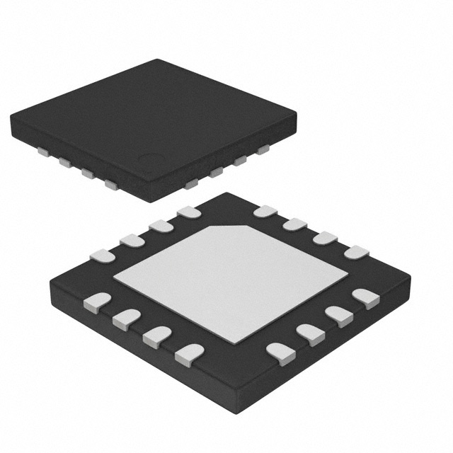


 工商网监
湘ICP备2023018690号
工商网监
湘ICP备2023018690号
