NOT RECOMMENDED FOR NEW DESIGNS
SY10E151
SY100E151
6-BIT D
REGISTER
Micrel, Inc.
SY10E151
SY100E151
DESCRIPTION
FEATURES
■ 1100MHz toggle frequency
■ Extended 100E VEE range of –4.2V to –5.46V
The SY10/100E151 offer 6 edge-triggered, high-speed,
master-slave D-type flip-flops with differential outputs,
designed for use in new, high-performance ECL systems.
The two external clock signals (CLK1, CLK2) are gated
through a logical OR operation before use as clocking
control for the flip-flops. Data is clocked into the flip-flops
on the rising edge of either CLK1 or CLK2 (or both). When
both CLK1 and CLK2 are at a logic LOW, data enters the
master and is transferred to the slave when either CLK1 or
CLK2 (or both) go HIGH.
The MR (Master Reset) signal operates asynchronously
to make all Q outputs go to a logic LOW.
■
■
■
■
Differential outputs
Asynchronous Master Reset
Dual clocks
Fully compatible with industry standard 10KH,
100K ECL levels
■ Internal 75KΩ input pulldown resistors
■ Fully compatible with Motorola MC10E/100E151
■ Available in 28-pin PLCC package
BLOCK DIAGRAM
PIN NAMES
Pin
D0
Q0
D
R
D1
Q1
D
R
D2
Data Inputs
CLK1, CLK2
Clock Inputs
MR
Master Reset
Q0–Q5
True Outputs
Q0–Q5
Inverting Outputs
VCCO
VCC to Output
Q2
Q3
Q4
D
R
D5
D0–D5
Q3
D
R
D4
Q1
Q2
D
R
D3
Q0
Function
Q4
Q5
D
R
Q5
CLK1
CLK2
M
R
M9999-052108
hbwhelp@micrel.com or (408) 955-1690
Rev.: H
1
Amendment: /0
Issue Date: May 2008
�SY10E151
SY100E151
Micrel, Inc.
Ordering Information(1)
VCCO
Q5
Q5
CLK1
NC
MR
CLK2
PACKAGE/ORDERING INFORMATION
25 24 23 22 21 20 19
D5
26
18
Q4
D4
D3
VEE
27
17
15
Q4
VCC
Q3
14
28
16
PLCC
TOP VIEW
J28-1
1
Part Number
Package
Type
Operating
Range
Package
Marking
Lead
Finish
SY10E151JI
J28-1
Industrial
SY10E151JI
Sn-Pb
SY10E151JITR(2)
J28-1
Industrial
SY10E151JI
Sn-Pb
SY10E151JC
J28-1
Commercial
SY10E151JC
Sn-Pb
SY10E151JCTR(2)
J28-1
Commercial
SY10E151JC
Sn-Pb
Q3
SY100E151JC
J28-1
Commercial
SY100E151JC
Sn-Pb
3
13
Q2
D0
Q2
J28-1
Commercial
SY100E151JC
Sn-Pb
4
12
SY100E151JCTR(2)
SY10E151JY(3)
J28-1
Industrial
SY10E151JY with
Pb-Free bar-line indicator
Matte-Sn
SY10E151JYTR(2, 3)
J28-1
Industrial
SY10E151JY with
Pb-Free bar-line indicator
Matte-Sn
SY100E151JZ(3)
J28-1
Commercial
SY100E151JZ with
Pb-Free bar-line indicator
Matte-Sn
SY100E151JZTR(2, 3)
J28-1
Commercial
SY100E151JZ with
Pb-Free bar-line indicator
Matte-Sn
7
8
9
10 11
VCCO
6
NC
VCCO
5
Q0
2
D1
Q0
Q1
Q1
D2
28-Pin PLCC (J28-1)
Notes:
1. Contact factory for die availability. Dice are guaranteed at TA = 25°C, DC Electricals only.
2. Tape and Reel.
3. Pb-Free package is recommended for new designs.
M9999-052108
hbwhelp@micrel.com or (408) 955-1690
2
�SY10E151
SY100E151
Micrel, Inc.
TRUTH TABLES(1)
Synchronous Operation
Asynchronous Operation
Inputs
Inputs
Output
Output
Dn
CLK1
CLK2
MR
Qn(t + 1)
Dn
CLK1
CLK2
MR
Qn(t + 1)
X
X
X
H
L
L
u
L
L
L
H
u
L
L
H
L
L
u
L
L
H
L
u
L
H
X
H
u
L
Qn(t)
X
u
H
L
Qn(t)
X
L
L
L
Qn(t)
Note:
1. H = HIGH Voltage Level
L = LOW Voltage Level
X = Don’t Care
t = Time before positive CLK transition
t+1 = Time after positive CLK transition
u = LOW-to-HIGH transition
DC ELECTRICAL CHARACTERISTICS(1)
VEE = VEE (Min.) to VEE (Max.); VCC = VCCO = GND
TA = 0°C
Symbol
Parameter
TA = +25°C
Min. Typ. Max. Min. Typ.
IIH
Input HIGH Current
IEE
Power Supply Current
10E
100E
TA = +85°C
Max. Min. Typ.
Max.
Unit
Condition
µA
—
mA
—
Max.
Unit
Condition
—
MHz
—
ps
—
—
—
150
—
—
150
—
—
150
—
—
65
65
78
78
—
—
65
65
78
78
—
—
65
75
78
90
Note:
1. Specification for packaged product only.
AC ELECTRICAL CHARACTERISTICS(2)
VEE = VEE (Min.) to VEE (Max.); VCC = VCCO = GND
TA = 0°C
Symbol
Parameter
TA = +25°C
Min. Typ. Max. Min. Typ.
—
1100 1400
TA = +85°C
Max. Min. Typ.
fMAX
Max. Toggle Frequency
1100 1400
—
1100 1400
tPD
Propagation Delay to Output
CLK
MR
475
475
650
650
800
850
475
475
650
650
800
850
475
475
650
650
800
850
0
–175
—
0
–175
—
0
–175
—
ps
—
tS
Set-up Time, D
tH
Hold Time, D
350
175
—
350
175
—
350
175
—
ps
—
tRR
Reset Recovery Time
750
550
—
750
550
—
750
550
—
ps
—
tPW
Minimum Pulse Width
CLK, MR
400
—
—
400
—
—
400
—
—
ps
—
tskew
Within-Device Skew
—
65
—
—
65
—
—
65
—
ps
1
tr
tf
Rise/Fall Time
20% to 80%
300
450
700
300
450
700
300
450
700
ps
—
Note:
1. Within-device skew is defined as identical transitions on similar paths through a device.
2. Specification for packaged product only.
M9999-052108
hbwhelp@micrel.com or (408) 955-1690
3
�SY10E151
SY100E151
Micrel, Inc.
28-PIN PLCC (J28-1)
Rev. 03
MICREL, INC. 2180 FORTUNE DRIVE SAN JOSE, CA 95131
TEL
+ 1 (408) 944-0800
FAX
+ 1 (408) 474-1000
WEB
USA
http://www.micrel.com
The information furnished by Micrel in this data sheet is believed to be accurate and reliable. However, no responsibility is assumed by Micrel for its use.
Micrel reserves the right to change circuitry and specifications at any time without notification to the customer.
Micrel Products are not designed or authorized for use as components in life support appliances, devices or systems where malfunction of a product can
reasonably be expected to result in personal injury. Life support devices or systems are devices or systems that (a) are intended for surgical implant into
the body or (b) support or sustain life, and whose failure to perform can be reasonably expected to result in a significant injury to the user. A Purchaser’s
use or sale of Micrel Products for use in life support appliances, devices or systems is at Purchaser’s own risk and Purchaser agrees to fully indemnify
Micrel for any damages resulting from such use or sale.
© 2006 Micrel, Incorporated.
M9999-052108
hbwhelp@micrel.com or (408) 955-1690
4
�
很抱歉,暂时无法提供与“SY10E151JI”相匹配的价格&库存,您可以联系我们找货
免费人工找货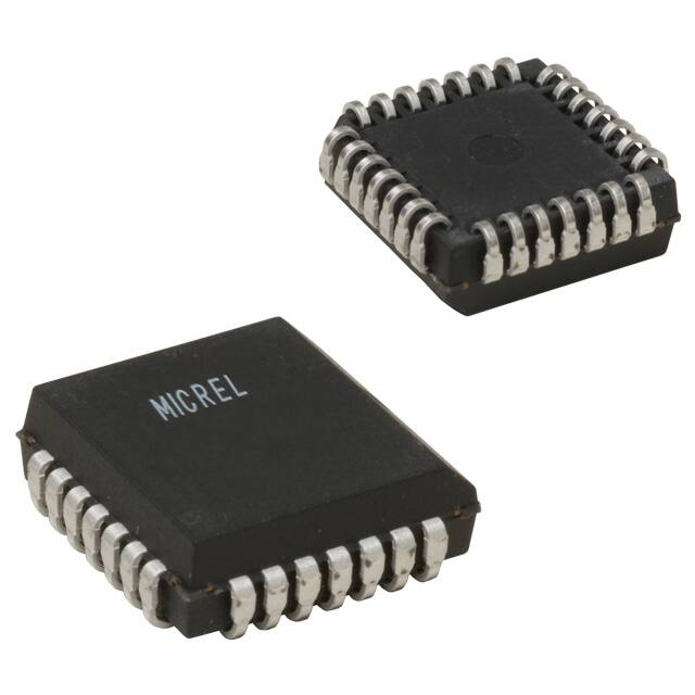


 工商网监
湘ICP备2023018690号
工商网监
湘ICP备2023018690号
