HMC723LC3C
v03.0514
HIGH SPEED LOGIC - SMT
13 Gbps, FAST RISE TIME D-TYPE FLIP-FLOP
w/ PROGRAMMABLE OUTPUT VOLTAGE
Typical Applications
Features
The HMC723LC3C is ideal for:
Supports High Data Rates: up to 13 Gbps
• RF ATE Applications
Differential & Singe-Ended Operation
• Broadband Test & Measurement
Fast Rise and Fall Times: 19 / 17 ps
• Serial Data Transmission up to 13 Gbps
Low Power Consumption: 260 mW typ.
• Digital Logic Systems up to 13 GHz
Programmable Differential
Output Voltage Swing: 700 - 1300 mV
Propagation Delay: 105 ps
Single Supply: -3.3V
16 Lead Ceramic 3x3mm SMT Package: 9mm 2
Functional Diagram
General Description
The HMC723LC3C is a D-type Flip Flop designed to
support data transmission rates of up to 13 Gbps, and
clock frequencies as high as 13 GHz. During normal
operation, data is transferred to the outputs on the
positive edge of the clock. Reversing the clock inputs
allows for negative-edge triggered applications. The
HMC723LC3C also features an output level control pin,
VR, which allows for loss compensation or for signal
level optimization.
All input signals to the HMC723LC3C are terminated with
50 Ohms to ground on-chip, and maybe either AC or DC
coupled. The differential outputs of the HMC723LC3C
may be either AC or DC coupled. Outputs can be
connected directly to a 50 Ohm to ground terminated
system, while DC blocking capacitors may be used if
the terminating system is 50 Ohms to a non-ground
DC voltage. The HMC723LC3C operates from a single
-3.3V DC supply and is available in a ceramic RoHS
compliant 3x3 mm SMT package.
Electrical Specifications, TA = +25°C, Vee = -3.3V
Parameter
Conditions
Power Supply Voltage
Min.
Typ.
Max
-3.6
-3.3
-3.0
V
Power Supply Current
80
mA
Maximum Data Rate
13
Gbps
Maximum Clock Rate
13
GHz
Input High Voltage
-0.5
0.5
Input Low Voltage
-1.0
0.0
Input Return Loss
Output Amplitude
Output High Voltage
1
Units
Frequency H
H
H - Positive voltage level
L - Negative voltage level
For price,
delivery
and
to place
orders:
Hittite
Corporation,
Elizabeth
Chelmsford,
MA
01824Inc.,
Information
furnished
by Analog
Devices
is believed
to be accurate
andMicrowave
reliable. However,
no
For price,2 delivery,
andDrive,
to place
orders: Analog
Devices,
responsibility is assumed by Analog Devices for its use, nor for any infringements of patents or other
One Technology Way, P.O. Box 9106, Norwood, MA 02062-9106
Phone:
978-250-3343
Fax:
978-250-3373
rights of third parties that may
result from
its use. Specifications subject
to change
without notice. No Order On-line at www.hittite.com
Phone: 781-329-4700 • Order online at www.analog.com
license is granted by implication or otherwise under any patent or patent rights of Analog Devices.
Application
Support:
Phone: 978-250-3343
or apps@hittite.com
Application
Support: Phone: 1-800-ANALOG-D
Trademarks and registered trademarks are
the property of their
respective owners.
4
�HMC723LC3C
v03.0514
13 Gbps, FAST RISE TIME D-TYPE FLIP-FLOP
w/ PROGRAMMABLE OUTPUT VOLTAGE
HIGH SPEED LOGIC - SMT
Absolute Maximum Ratings
Power Supply Voltage (Vee)
-3.75V to +0.5V
Input Signals
-2V to +0.5V
Output Signals
-1.5V to +1V
Storage Temperature
-65°C to +150°C
Operating Temperature
-40°C to +85°C
ELECTROSTATIC SENSITIVE DEVICE
OBSERVE HANDLING PRECAUTIONS
Outline Drawing
NOTES:
1. PACKAGE BODY MATERIAL: ALUMINA
2. LEAD AND GROUND PADDLE PLATING:
30-80 MICROINCHES GOLD OVER 50 MICROINCHES MINIMUM NICKEL.
3. DIMENSIONS ARE IN INCHES [MILLIMETERS].
4. LEAD SPACING TOLERANCE IS NON-CUMULATIVE.
5. PACKAGE WARP SHALL NOT EXCEED 0.05mm DATUM -C6. ALL GROUND LEADS MUST BE SOLDERED TO PCB RF GROUND.
7. GROUND PADDLE MUST BE SOLDERED TO Vee.
Package Information
Part Number
Package Body Material
Lead Finish
HMC723LC3C
Alumina, White
Gold over Nickel
MSL Rating
MSL3
[1]
Package Marking [2]
H723
XXXX
[1] Max peak reflow temperature of 260 °C
[2] 4-Digit lot number XXXX
5
Information
furnished
by Analog
Devices
is believed
to be accurate
andMicrowave
reliable. However,
no
For price,
delivery
and
to place
orders:
Hittite
Corporation,
Elizabeth
01824
For price,2delivery,
and Drive,
to placeChelmsford,
orders: AnalogMA
Devices,
Inc.,
responsibility is assumed by Analog Devices for its use, nor for any infringements of patents or other
One Technology Way, P.O. Box 9106, Norwood, MA 02062-9106
Phone:
Fax:
978-250-3373
rights of third parties that may
result from978-250-3343
its use. Specifications subject
to change
without notice. No Order On-line at www.hittite.com
Phone: 781-329-4700 • Order online at www.analog.com
license is granted by implication or otherwise under any patent or patent rights of Analog Devices.
Application
Support:
Phone: 978-250-3343
or apps@hittite.com
Application
Support: Phone: 1-800-ANALOG-D
Trademarks and registered trademarks are
the property of their
respective owners.
�HMC723LC3C
v03.0514
13 Gbps, FAST RISE TIME D-TYPE FLIP-FLOP
w/ PROGRAMMABLE OUTPUT VOLTAGE
Pin Descriptions
Function
Description
1, 4, 5, 8, 9, 12
GND
Signal Grounds
2, 3
DN, DP
Data Inputs
6, 7
CP, CN
Clock Inputs
10, 11
QN, QP
Data Outputs
13, 16
GND
Supply Ground
14
VR
Output level control. Output level may be adjusted by
either applying a voltage to VR per “Output Differential
vs. VR” plot, or by tying VR to GND with a resistor per the
following equation: V0(R) = 1.2 / (2.1 + R), R in kΩ
15, Package
Base
Vee
Negative Supply
Interface Schematic
For price,
delivery
and
to place
orders:
HittiteandMicrowave
Corporation,
Elizabeth
Chelmsford,
MA
01824Inc.,
Information
furnished
by Analog
Devices
is believed
to be accurate
reliable. However,
no
For price,2 delivery,
andDrive,
to place
orders: Analog
Devices,
responsibility is assumed by Analog Devices for its use, nor for any infringements of patents or other
One Technology Way, P.O. Box 9106, Norwood, MA 02062-9106
Phone:
978-250-3343
Fax:
978-250-3373
rights of third parties that may
result from
its use. Specifications subject
to change
without notice. No Order On-line at www.hittite.com
Phone: 781-329-4700 • Order online at www.analog.com
license is granted by implication or otherwise under any patent or patent rights of Analog Devices.
Application
Support:
Phone: 978-250-3343
or apps@hittite.com
Application
Support: Phone: 1-800-ANALOG-D
Trademarks and registered trademarks are
the property of their
respective owners.
HIGH SPEED LOGIC - SMT
Pin Number
6
�HMC723LC3C
v03.0514
13 Gbps, FAST RISE TIME D-TYPE FLIP-FLOP
w/ PROGRAMMABLE OUTPUT VOLTAGE
HIGH SPEED LOGIC - SMT
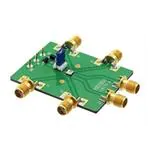
Evaluation PCB
Item
Description
J1
DN
J2
DP
J3
CP
J4
CN
J5
QN
J6
QP
J7
Vee
J8
VR
J9
GND
List of Materials for Evaluation PCB 118777 [1]
Item
Description
J1 - J6
PCB Mount SMA RF Connectors
J7 - J9
DC Pin
C1, C2
100 pF Capacitor, 0402 Pkg.
C3, C4
4.7 µF Capacitor, Tantalum
R1
10 Ohm Resistor, 0603 Pkg.
U1
HMC723LC3C
High Speed Logic, D-Type Flip-Flop
PCB [2]
118775 Evaluation Board
[1] Reference this number when ordering complete evaluation PCB
[2] Circuit Board Material: Rogers 4350
7
The circuit board used in the application should use
RF circuit design techniques. Signal lines should
have 50 Ohm impedance while the package ground leads should be connected directly to the
ground plane similar to that shown. The exposed
package base should be connected to Vee. A sufficient number of via holes should be used to connect
the top and bottom ground planes. The evaluation
circuit board shown is available from Hittite upon
request.
Information
furnished
by Analog
is believed
to be accurate
reliable. However,
no
For
price,
delivery
andDevices
to place
orders:
Hittiteand
Microwave
Corporation,
2 Elizabeth
Drive,
Chelmsford,
MADevices,
01824 Inc.,
For price,
delivery, and
to place
orders: Analog
responsibility is assumed by Analog Devices for its use, nor for any infringements of patents or other
One Technology Way, P.O. Box 9106, Norwood, MA 02062-9106
978-250-3343
Fax:to978-250-3373
rights of third parties that Phone:
may result from
its use. Specifications subject
change without notice. No Order On-line at www.hittite.com
Phone: 781-329-4700 • Order online at www.analog.com
license is granted by implication or otherwise under any patent or patent rights of Analog Devices.
or apps@hittite.com
Application
Support: Phone: 1-800-ANALOG-D
Trademarks and registered trademarksApplication
are the property ofSupport:
their respectivePhone:
owners. 978-250-3343
�HMC723LC3C
v03.0514
13 Gbps, FAST RISE TIME D-TYPE FLIP-FLOP
w/ PROGRAMMABLE OUTPUT VOLTAGE
HIGH SPEED LOGIC - SMT
Application Circuit
For price,
delivery
and
to place
orders:
HittiteandMicrowave
Corporation,
Elizabeth
Chelmsford,
MA
01824Inc.,
Information
furnished
by Analog
Devices
is believed
to be accurate
reliable. However,
no
For price,2 delivery,
andDrive,
to place
orders: Analog
Devices,
responsibility is assumed by Analog Devices for its use, nor for any infringements of patents or other
One Technology
P.O. Box 9106, Norwood, MA 02062-9106
Phone: 978-250-3343
Fax: 978-250-3373
Order
On-line Way,
at www.hittite.com
rights of third parties that may result from its use. Specifications subject to change without notice. No
Phone: 781-329-4700 • Order online at www.analog.com
license is granted by implication or otherwise
under any patent
or patentPhone:
rights of Analog
Devices.
Application
Support:
978-250-3343
or apps@hittite.com
Application Support: Phone: 1-800-ANALOG-D
Trademarks and registered trademarks are the property of their respective owners.
8
�


 工商网监
湘ICP备2023018690号
工商网监
湘ICP备2023018690号
