REVISIONS
LTR
DESCRIPTION
DATE (YR-MO-DA)
APPROVED
A
Changes in accordance with N.O.R 5962-R319-92.
92-09-30
M. A. FRYE
B
Drawing updated to reflect current requirements. Add theta JC to 1.3. Make
change to -ISC and +ISC tests as specified under table I. –ro
00-08-28
R. MONNIN
Replaced reference to MIL-STD-973 with reference to MIL-PRF-38535. -rrp
03-12-17
R. MONNIN
C
THE ORIGINAL FIRST SHEET OF THIS DRAWING HAS BEEN REPLACED.
REV
SHEET
REV
SHEET
REV STATUS
REV
C
C
C
C
C
C
C
C
OF SHEETS
SHEET
1
2
3
4
5
6
7
8
PMIC N/A
PREPARED BY
MARCIA B. KELLEHER
STANDARD
MICROCIRCUIT
DRAWING
THIS DRAWING IS AVAILABLE
FOR USE BY ALL
DEPARTMENTS
AND AGENCIES OF THE
DEPARTMENT OF DEFENSE
AMSC N/A
DEFENSE SUPPLY CENTER COLUMBUS
COLUMBUS, OHIO 43216
http://www.dscc.dla.mil
CHECKED BY
D. A. DiCENZO
APPROVED BY
N. A. HAUCK
MICROCIRCUIT, LINEAR, DUAL MATCHED HIGH
PERFORMANCE OPERATIONAL AMPLIFIERS,
MONOLITHIC SILICON
DRAWING APPROVAL DATE
87-09-15
REVISION LEVEL
C
SIZE
CAGE CODE
A
67268
SHEET
DSCC FORM 2233
APR 97
DISTRIBUTION STATEMENT A. Approved for public release; distribution is unlimited.
1 OF
5962-87714
8
5962-E085-04
�1. SCOPE
1.1 Scope. This drawing describes device requirements for MIL-STD-883 compliant, non-JAN class level B microcircuits in
accordance with MIL-PRF-38535, appendix A.
1.2 Part or Identifying Number (PIN). The complete PIN is as shown in the following example:
5962-87714
01
G
X
Drawing number
Device type
(see 1.2.1)
Case outline
(see 1.2.2)
Lead finish
(see 1.2.3)
1.2.1 Device type(s). The device type(s) identify the circuit function as follows:
Device type
Generic number
Circuit function
01
OP-14A
02
OP-14B
Dual matched high performance
operational amplifiers
Dual matched high performance
operational amplifiers
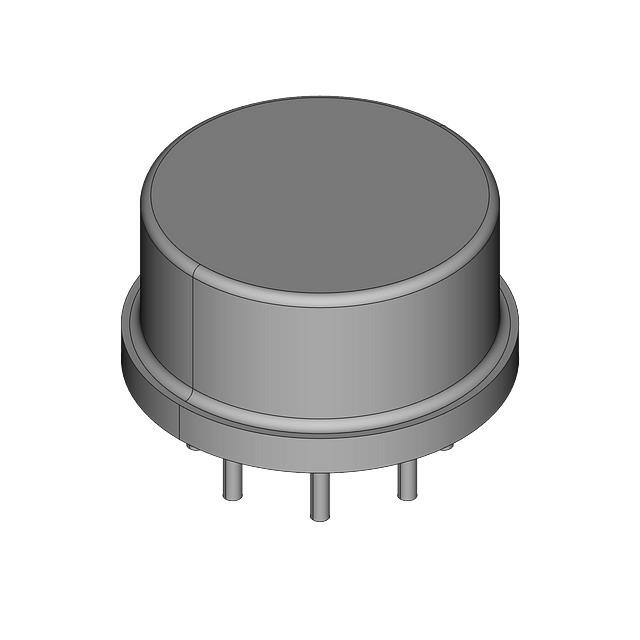
1.2.2 Case outline(s). The case outline(s) are as designated in MIL-STD-1835 and as follows:
Outline letter
Descriptive designator
Terminals
Package style
G
MACY1-X8
8
P
GDIP1-T8 or CDIP2-T8
8
1.2.3 Lead finish. The lead finish is as specified in MIL-PRF-38535, appendix A.
Can
Dual-in-line
1.3 Absolute maximum ratings.
Supply voltage (VS) ...................................................................................................
Power dissipation (PD) ..............................................................................................
Differential input voltage ...........................................................................................
Input voltage .............................................................................................................
Output short-circuit duration .....................................................................................
Storage temperature range .......................................................................................
Lead temperature range (soldering, 60 seconds) .....................................................
Junction temperature (TJ) .........................................................................................
Thermal resistance, junction-to-case (θJC) ................................................................
±22 V
500 mW
±30 V
Supply voltage
Indefinite
-65°C to +150°C
+300°C
-65°C to +150°C
See MIL-STD-1835
1.4 Recommended operating conditions.
Supply voltage (VS) ................................................................................................... ±15 V
Ambient operating temperature range (TA) ............................................................... -55°C to +125°C
STANDARD
MICROCIRCUIT DRAWING
DEFENSE SUPPLY CENTER COLUMBUS
COLUMBUS, OHIO 43216-5000
DSCC FORM 2234
APR 97
SIZE
5962-87714
A
REVISION LEVEL
C
SHEET
2
�2. APPLICABLE DOCUMENTS
2.1 Government specification, standards, and handbooks. The following specification, standards, and handbooks form a
part of this drawing to the extent specified herein. Unless otherwise specified, the issues of these documents are those listed
in the issue of the Department of Defense Index of Specifications and Standards (DoDISS) and supplement thereto, cited in
the solicitation.
SPECIFICATION
DEPARTMENT OF DEFENSE
MIL-PRF-38535 -- Integrated Circuits, Manufacturing, General Specification for.
STANDARDS
DEPARTMENT OF DEFENSE
MIL-STD-883 MIL-STD-1835 -
Test Method Standard Microcircuits.
Interface Standard Electronic Component Case Outlines.
HANDBOOKS
DEPARTMENT OF DEFENSE
MIL-HDBK-103 -- List of Standard Microcircuit Drawings.
MIL-HDBK-780 - Standard Microcircuit Drawings.
(Unless otherwise indicated, copies of the specification, standards, and handbooks are available from the Standardization
Document Order Desk, 700 Robbins Avenue, Building 4D, Philadelphia, PA 19111-5094.)
2.2 Order of precedence. In the event of a conflict between the text of this drawing and the references cited herein, the text
of this drawing takes precedence. Nothing in this document, however, supersedes applicable laws and regulations unless a
specific exemption has been obtained.
3. REQUIREMENTS
3.1 Item requirements. The individual item requirements shall be in accordance with MIL-PRF-38535, appendix A for nonJAN class level B devices and as specified herein. Product built to this drawing that is produced by a Qualified Manufacturer
Listing (QML) certified and qualified manufacturer or a manufacturer who has been granted transitional certification to MILPRF-38535 may be processed as QML product in accordance with the manufacturers approved program plan and qualifying
activity approval in accordance with MIL-PRF-38535. This QML flow as documented in the Quality Management (QM) plan
may make modifications to the requirements herein. These modifications shall not affect form, fit, or function of the device.
These modifications shall not affect the PIN as described herein. A "Q" or "QML" certification mark in accordance with MILPRF-38535 is required to identify when the QML flow option is used.
3.2 Design, construction, and physical dimensions. The design, construction, and physical dimensions shall be as
specified in MIL-PRF-38535, appendix A and herein.
3.2. Case outline(s). The case outline(s) shall be in accordance with 1.2.2 herein.
3.2.1 Terminal connections. The terminal connections shall be as specified on figure 1.
3.3 Electrical performance characteristics. Unless otherwise specified herein, the electrical performance characteristics are
as specified in table I and shall apply over the full ambient operating temperature range.
3.4 Electrical test requirements. The electrical test requirements shall be the subgroups specified in table II. The electrical
tests for each subgroup are described in table I.
3.5 Marking. Marking shall be in accordance with MIL-PRF-38535, appendix A. The part shall be marked with the PIN
listed in 1.2 herein. In addition, the manufacturer's PIN may also be marked as listed in MIL-HDBK-103 (see 6.6 herein). For
packages where marking of the entire SMD PIN number is not feasible due to space limitations, the manufacturer has the
option of not marking the "5962-" on the device.
STANDARD
MICROCIRCUIT DRAWING
DEFENSE SUPPLY CENTER COLUMBUS
COLUMBUS, OHIO 43216-5000
DSCC FORM 2234
APR 97
SIZE
5962-87714
A
REVISION LEVEL
C
SHEET
3
�TABLE I. Electrical performance characteristics.
Test
Input offset voltage
Symbol
Conditions
-55°C ≤ TA ≤ +125°C
VS = ±15 V
unless otherwise specified
VOS
RS ≤ 20 kΩ
Group A
subgroups
Device
type
1
01
Limits
2, 3
1
02
2, 3
Input offset current
IOS
1
01
2, 3
1
02
2, 3
Input bias current
IB
1
1
IVR
1/
Common mode rejection
ratio
CMRR
VCM = IVR = ±10 V,
Power supply rejection ratio
PSRR
Output voltage swing
VO
RS ≤ 20 kΩ
AVO
VO = ±10 V, RL ≥ 2 kΩ
-5
5
-10
10
-25
25
-60
60
02
-100
100
-200
200
nA
nA
±10
V
1
01
85
dB
80
1, 2, 3
02
1, 2, 3
01
60
70
02
150
4, 5, 6
01
±12
4
02
±12
01
100
4
µV/V
V
±10
V/mV
50
50
02
5, 6
No load each amplifier,
6
mV
All
4
ISY
5
-6
50
5, 6
Power supply current
-5
50
5, 6
Large signal voltage gain
1.5
1, 2, 3
RS ≤ 20 kΩ
RL ≥ 2 kΩ
-1.5
-50
2, 3
VS = ±5 V to ±20 V,
Max
0.75
01
2, 3
Input voltage range
Min
-0.75
-50
2, 3
Unit
25
1
All
3
mA
1
All
90
mW
TA = +25°C
Power dissipation
PD
No load each amplifier,
TA = +25°C
Channel separation
Output short circuit current
CS
-ISC
7
TA = +25°C
1
TA = +25°C
01
100
02
80
All
-60
+ISC
Input resistance differential
mode
RIN
dB
mA
60
1
TA = +25°C 2/
01
2.0
02
1.0
MΩ
See footnotes at end of table.
STANDARD
MICROCIRCUIT DRAWING
DEFENSE SUPPLY CENTER COLUMBUS
COLUMBUS, OHIO 43216-5000
DSCC FORM 2234
APR 97
SIZE
5962-87714
A
REVISION LEVEL
C
SHEET
4
�TABLE I. Electrical performance characteristics – Continued.
Test
Symbol
Conditions
-55°C ≤ TA ≤ +125°C
VS = ±15 V
unless otherwise specified
tr
AVCL = +1, VIN = 50 mV,
Group A
subgroups
Device
type
Limits
9
All
Max
350
ns
9
All
10
%
7
All
0.25
V/µs
Min
Rise time
Unit
RL ≥ 2 kΩ, RS = 50 Ω,
CL = 50 pF, TA = +25°C
Overshoot
OS
AVCL = +1, VIN = 50 mV,
RL ≥ 2 kΩ, RS = 50 Ω,
CL = 50 pF, TA = +25°C
Slew rate
SR
RL ≥ 2 kΩ, RS = 50 kΩ,
CL = 100 pF, TA = +25°C
Bandwidth
BW
AVCL = +1, TA = +25°C 3/
7
All
1
MHz
Large signal bandwidth
LSBW
VO = 20 VP-P,
7
All
4
kHz
Input offset voltage match
∆VOS
1
All
-1
1
-1.5
1.5
Common mode rejection
match
∆CMRR
All
94
4/
TA = +25°C
2, 3
VCM = ±10 V, RS ≤ 100 Ω
1
2, 3
mV
dB
90
1/ IVR is guaranteed by CMRR test.
2/ RIN is guaranteed by IB test. RIN = 4 kT/qIB where kT/q = 0.026 at +25°C.
3/ Bandwidth is guaranteed by tr test. BW = 0.35/ tr.
4/ Large signal bandwidth is guaranteed by SR test. LSBW = SR/(2 x π x VPEAK).
3.5.1 Certification/compliance mark. A compliance indicator “C” shall be marked on all non-JAN devices built in compliance
to MIL-PRF-38535, appendix A. The compliance indicator “C” shall be replaced with a "Q" or "QML" certification mark in
accordance with MIL-PRF-38535 to identify when the QML flow option is used.
3.6 Certificate of compliance. A certificate of compliance shall be required from a manufacturer in order to be listed as an
approved source of supply in MIL-HDBK-103 (see 6.6 herein). The certificate of compliance submitted to DSCC-VA prior to
listing as an approved source of supply shall affirm that the manufacturer's product meets the requirements of MIL-PRF38535, appendix A and the requirements herein.
3.7 Certificate of conformance. A certificate of conformance as required in MIL-PRF-38535, appendix A shall be provided
with each lot of microcircuits delivered to this drawing.
3.8 Notification of change. Notification of change to DSCC-VA shall be required in accordance with MIL-PRF-38535,
appendix A.
3.9 Verification and review. DSCC, DSCC's agent, and the acquiring activity retain the option to review the manufacturer's
facility and applicable required documentation. Offshore documentation shall be made available onshore at the option of the
reviewer.
STANDARD
MICROCIRCUIT DRAWING
DEFENSE SUPPLY CENTER COLUMBUS
COLUMBUS, OHIO 43216-5000
DSCC FORM 2234
APR 97
SIZE
5962-87714
A
REVISION LEVEL
C
SHEET
5
�Device types
Case outlines
Terminal number
1
2
3
4
5
6
7
8
01 and 02
G and P
Terminal symbol
OUT A
-IN A
+IN A
-VS
+IN B
-IN B
OUT B
+VS
FIGURE 1. Terminal connections.
STANDARD
MICROCIRCUIT DRAWING
DEFENSE SUPPLY CENTER COLUMBUS
COLUMBUS, OHIO 43216-5000
DSCC FORM 2234
APR 97
SIZE
5962-87714
A
REVISION LEVEL
C
SHEET
6
�4. QUALITY ASSURANCE PROVISIONS
4.1 Sampling and inspection. Sampling and inspection procedures shall be in accordance with MIL-PRF-38535,
appendix A.
4.2 Screening. Screening shall be in accordance with method 5004 of MIL-STD-883, and shall be conducted on all devices
prior to quality conformance inspection. The following additional criteria shall apply:
a.
Burn-in test, method 1015 of MIL-STD-883.
(1) Test condition A, B, C, or D. The test circuit shall be maintained by the manufacturer under document revision
level control and shall be made available to the preparing or acquiring activity upon request. The test circuit shall
specify the inputs, outputs, biases, and power dissipation, as applicable, in accordance with the intent specified in
test method 1015 of MIL-STD-883.
(2) TA = +125°C, minimum.
b.
Interim and final electrical test parameters shall be as specified in table II herein, except interim electrical parameter
tests prior to burn-in are optional at the discretion of the manufacturer.
4.3 Quality conformance inspection. Quality conformance inspection shall be in accordance with method 5005 of MIL-STD883 including groups A, B, C, and D inspections. The following additional criteria shall apply.
4.3.1 Group A inspection.
a.
Tests shall be as specified in table II herein.
b.
Subgroups 8, 10, and 11 in table I, method 5005 of MIL-STD-883 shall be omitted.
4.3.2 Groups C and D inspections.
a.
End-point electrical parameters shall be as specified in table II herein.
b.
Steady-state life test conditions, method 1005 of MIL-STD-883.
(1)
Test condition A, B, C, or D. The test circuit shall be maintained by the manufacturer under document revision
level control and shall be made available to the preparing or acquiring activity upon request. The test circuit
shall specify the inputs, outputs, biases, and power dissipation, as applicable, in accordance with the intent
specified in test method 1005 of MIL-STD-883.
(2)
TA = +125°C, minimum.
(3)
Test duration: 1,000 hours, except as permitted by method 1005 of MIL-STD-883.
STANDARD
MICROCIRCUIT DRAWING
DEFENSE SUPPLY CENTER COLUMBUS
COLUMBUS, OHIO 43216-5000
DSCC FORM 2234
APR 97
SIZE
5962-87714
A
REVISION LEVEL
C
SHEET
7
�TABLE II. Electrical test requirements.
MIL-STD-883 test requirements
Interim electrical parameters
(method 5004)
Final electrical test parameters
(method 5004)
Group A test requirements
(method 5005)
Groups C and D end-point
electrical parameters
(method 5005)
Subgroups
(in accordance with
MIL-STD-883, method 5005,
table I)
1
1*, 2, 3, 4, 5, 6
1, 2, 3, 4, 5, 6, 7, 9
1
* PDA applies to subgroup 1.
5. PACKAGING
5.1 Packaging requirements. The requirements for packaging shall be in accordance with MIL-PRF-38535, appendix A.
6. NOTES
6.1 Intended use. Microcircuits conforming to this drawing are intended for use for Government microcircuit applications
(original equipment), design applications, and logistics purposes.
6.2 Replaceability. Microcircuits covered by this drawing will replace the same generic device covered by a contractorprepared specification or drawing.
6.3 Configuration control of SMD's. All proposed changes to existing SMD's will be coordinated with the users of record for
the individual documents. This coordination will be accomplished using DD Form 1692, Engineering Change Proposal.
6.4 Record of users. Military and industrial users shall inform Defense Supply Center Columbus when a system application
requires configuration control and the applicable SMD. DSCC will maintain a record of users and this list will be used for
coordination and distribution of changes to the drawings. Users of drawings covering microelectronics devices (FSC 5962)
should contact DSCC-VA, telephone (614) 692-0544.
6.5 Comments. Comments on this drawing should be directed to DSCC-VA, Columbus, Ohio 43216-5000, or telephone
(614) 692-0547.
6.6 Approved sources of supply. Approved sources of supply are listed in MIL-HDBK-103. The vendors listed in MILHDBK-103 have agreed to this drawing and a certificate of compliance (see 3.6 herein) has been submitted to and accepted
by DSCC-VA.
STANDARD
MICROCIRCUIT DRAWING
DEFENSE SUPPLY CENTER COLUMBUS
COLUMBUS, OHIO 43216-5000
DSCC FORM 2234
APR 97
SIZE
5962-87714
A
REVISION LEVEL
C
SHEET
8
�STANDARD MICROCIRCUIT DRAWING BULLETIN
DATE: 03-12-17
Approved sources of supply for SMD 5962-87714 are listed below for immediate acquisition information only and
shall be added to MIL-HDBK-103 and QML-38535 during the next revision. MIL-HDBK-103 and QML-38535 will be
revised to include the addition or deletion of sources. The vendors listed below have agreed to this drawing and a
certificate of compliance has been submitted to and accepted by DSCC-VA. This bulletin is superseded by the next
dated revision of MIL-HDBK-103 and QML-38535.
Standard
microcircuit drawing
PIN 1/
5962-8771401GA
5962-8771401PA
5962-8771402GA
5962-8771402PA
Vendor
CAGE
number
3/
3/
3/
3/
Vendor
similar
PIN 2/
OP-14AJ/883
OP-14AZ/883
OP-14BJ/883
OP-14BZ/883
1/ The lead finish shown for each PIN representing
a hermetic package is the most readily available
from the manufacturer listed for that part. If the
desired lead finish is not listed contact the vendor
to determine its availability.
2/ Caution. Do not use this number for item
acquisition. Items acquired to this number may not
satisfy the performance requirements of this drawing.
3/ Not available from an approved source of supply.
The information contained herein is disseminated for convenience only and the
Government assumes no liability whatsoever for any inaccuracies in the
information bulletin.
�


 工商网监
湘ICP备2023018690号
工商网监
湘ICP备2023018690号
