11-Bit/16-Bit, 12 GSPS,
RF Digital-to-Analog Converters
AD9161/AD9162
Data Sheet
In baseband mode, wide bandwidth capability combines with
high dynamic range to support DOCSIS 3.1 cable infrastructure
compliance from the minimum of two carriers to full maximum
spectrum of 1.794 GHz. A 2× interpolator filter (FIR85) enables
the AD9161/AD9162 to be configured for lower data rates and
converter clocking to reduce the overall system power and ease
the filtering requirements. In Mix-Mode™ operation, the AD9161/
AD9162 can reconstruct RF carriers in the second and third
Nyquist zones up to 7.5 GHz while still maintaining exceptional
dynamic range. The output current can be programmed from
8 mA to 38.76 mA. The AD9161/AD9162 data interface consists
of up to eight JESD204B serializer/deserializer (SERDES) lanes
that are programmable in terms of lane speed and number of
lanes to enable application flexibility.
FEATURES
DAC update rate up to 12 GSPS (minimum)
Direct RF synthesis at 6 GSPS (minimum)
DC to 2.5 GHz in baseband 1× bypass mode
DC to 6 GHz in 2× nonreturn-to-zero (NRZ) mode
1.5 GHz to 7.5 GHz in Mix-Mode
Bypassable interpolation (1× or bypass mode)
2×, 3×, 4×, 6×, 8×, 12×, 16×, 24×
Excellent dynamic performance
APPLICATIONS
Broadband communications systems
DOCSIS 3.1 cable modem termination system (CMTS)/
video on demand (VOD)/edge quadrature amplitude
modulation (EQAM)
Wireless communications infrastructure
W-CDMA, LTE, LTE-A, point to point
Instrumentation, automatic test equipment (ATE)
Radars and jammers
A serial peripheral interface (SPI) can configure the AD9161/
AD9162 and monitor the status of all registers. The AD9161/
AD9162 are offered in an 165-ball, 8.0 mm × 8.0 mm, 0.5 mm
pitch, CSP_BGA package and in an 169-ball, 11 mm × 11 mm,
0.8 mm pitch, CSP_BGA package, including a leaded ball
option for the AD9162.
GENERAL DESCRIPTION
PRODUCT HIGHLIGHTS
The AD9161/AD91621 are high performance, 11-bit/16-bit
digital-to-analog converters (DACs) that supports data rates to
6 GSPS. The DAC core is based on a quad-switch architecture
coupled with a 2× interpolator filter that enables an effective
DAC update rate of up to 12 GSPS in some modes. The high
dynamic range and bandwidth makes these DACs ideally suited
for the most demanding high speed radio frequency (RF) DAC
applications.
1.
2.
3.
High dynamic range and signal reconstruction bandwidth
supports RF signal synthesis of up to 7.5 GHz.
Up to eight lanes JESD204B SERDES interface flexible in
terms of number of lanes and lane speed.
Bandwidth and dynamic range to meet DOCSIS 3.1
compliance with margin.
FUNCTIONAL BLOCK DIAGRAM
RESET
IRQ
ISET VREF
AD9161/AD9162
SPI
VREF
NRZ RZ MIX
SERDIN0±
SYSREF±
HB
2×
JESD
HB
2×
HB
3×
HB
2×,
4×,
8×
NCO
TO JESD
TO DATAPATH
TX_ENABLE
INV
SINC
DAC
CORE
OUTPUT±
CLOCK
DISTRIBUTION
CLK±
14379-001
SERDIN7±
SYNCOUT±
DATA
LATCH
SDIO
SDO
CS
SCLK
Figure 1.
1
Protected by U.S. Patents 6,842,132 and 7,796,971.
Rev. D
Document Feedback
Information furnished by Analog Devices is believed to be accurate and reliable. However, no
responsibility is assumed by Analog Devices for its use, nor for any infringements of patents or other
rights of third parties that may result from its use. Specifications subject to change without notice. No
license is granted by implication or otherwise under any patent or patent rights of Analog Devices.
Trademarks and registered trademarks are the property of their respective owners.
One Technology Way, P.O. Box 9106, Norwood, MA 02062-9106, U.S.A.
Tel: 781.329.4700 ©2016–2019 Analog Devices, Inc. All rights reserved.
Technical Support
www.analog.com
�AD9161/AD9162
Data Sheet
TABLE OF CONTENTS
Features .............................................................................................. 1
JESD204B Overview .................................................................. 46
Applications ....................................................................................... 1
Physical Layer ............................................................................. 47
General Description ......................................................................... 1
Data Link Layer .......................................................................... 50
Product Highlights ........................................................................... 1
Transport Layer .......................................................................... 58
Functional Block Diagram .............................................................. 1
JESD204B Test Modes ............................................................... 60
Revision History ............................................................................... 3
JESD204B Error Monitoring..................................................... 62
Specifications..................................................................................... 4
Hardware Considerations ......................................................... 64
DC Specifications ......................................................................... 4
Main Digital Datapath ................................................................... 65
DAC Input Clock Overclocking Specifications ........................ 5
Data Format ................................................................................ 65
Power Supply DC Specifications ................................................ 5
Interpolation Filters ................................................................... 65
Serial Port and CMOS Pin Specifications ................................. 8
Digital Modulation ..................................................................... 68
JESD204B Serial Interface Speed Specifications ...................... 9
Inverse Sinc ................................................................................. 70
SYSREF± to DAC Clock Timing Specifications ....................... 9
Downstream Protection ............................................................ 70
Digital Input Data Timing Specifications ............................... 10
Datapath PRBS ........................................................................... 71
JESD204B Interface Electrical Specifications ......................... 10
Datapath PRBS IRQ ................................................................... 71
AC Specifications........................................................................ 11
Interrupt Request Operation ........................................................ 73
Absolute Maximum Ratings.......................................................... 13
Interrupt Service Routine .......................................................... 73
Reflow Profile .............................................................................. 13
Applications Information .............................................................. 74
Thermal Management ............................................................... 13
Hardware Considerations ......................................................... 74
Thermal Resistance .................................................................... 13
Analog Interface Considerations .................................................. 77
ESD Caution ................................................................................ 13
Analog Modes of Operation ..................................................... 77
Pin Configurations and Function Descriptions ......................... 14
Clock Input.................................................................................. 78
Typical Performance Characteristics ........................................... 18
Shuffle Mode ............................................................................... 79
AD9161 ........................................................................................ 18
DLL............................................................................................... 79
AD9162 ........................................................................................ 28
Voltage Reference ....................................................................... 79
Terminology .................................................................................... 42
Temperature Sensor ................................................................... 80
Theory of Operation ...................................................................... 43
Analog Outputs .......................................................................... 80
Serial Port Operation ..................................................................... 44
Start-Up Sequence .......................................................................... 82
Data Format ................................................................................ 44
Register Summary .......................................................................... 84
Serial Port Pin Descriptions ...................................................... 44
Register Details ............................................................................... 91
Serial Port Options ..................................................................... 44
Outline Dimensions ..................................................................... 143
JESD204B Serial Data Interface .................................................... 46
Ordering Guide ........................................................................ 144
Rev. D | Page 2 of 144
�Data Sheet
AD9161/AD9162
REVISION HISTORY
5/2019—Rev. C to Rev. D
Changes to INPUTS (SDIO, SCLK, CS, RESET, TX_ENABLE)
Parameters, Table 4 ........................................................................... 8
Changes to Table 11 ........................................................................13
Change to Figure 30 Caption .........................................................22
Change to Transport Layer Testing Section.................................61
Changes to Data Format Section...................................................65
Deleted Table 38; Renumbered Sequentially ...............................70
Changes to Changing the Main NCO Frequency Section .........70
Changes to Peak DAC Output Power Capability Section ..........80
Changes to Table 42 ........................................................................83
Change to Register 0x280 Value Column, Table 43 ....................84
Changes to Table 45 ........................................................................86
Changes to Table 46 ........................................................................93
Updated Outline Dimensions ......................................................143
9/2016—Rev. 0 to Rev. A
Changes to Table 1 ............................................................................ 3
Change to AC Specifications Section ........................................... 10
Added Reflow Profile Section, Thermal Management Section,
and Figure 3, Renumbered Sequentially ...................................... 12
Changes to Figure 80 ...................................................................... 30
Changes to Link Delay Setup Example, With Known Delays
Section .............................................................................................. 54
Changes to Table 25 ........................................................................ 57
Moved Figure 188............................................................................ 77
Added Temperature Sensor Section ............................................. 78
Changes to Table 46 ........................................................................ 87
Changes to Table 47 ........................................................................ 99
Changes to Ordering Guide .........................................................139
5/2016—Revision 0: Initial Version
7/2017—Rev. B to Rev. C
Changes to Thermal Management Section and Thermal
Resistance Section ...........................................................................13
Changes to Table 46 ........................................................................89
Changes to Table 47 ......................................................................134
4/2017—Rev. A to Rev. B
Change to OUTPUT ± to VNEG_NIP2 Parameter, Table 11........13
Changes to Figure 153 ....................................................................53
Changes to Link Delay Setup Examples, with Known Delays
Section ..............................................................................................55
Changes to Link Delay Setup Examples, without Known Delays
Section ..............................................................................................56
Changes to Table 31 ........................................................................61
Added Datapath PRBS Section......................................................71
Added Datapath PRBS IRQ Section .............................................72
Changes to Equivalent DAC Output and Transfer Function
Section ..............................................................................................80
Changes to Output Stage Configuration Section ........................81
Change to Register 0x230, Table 47 ............................................101
Rev. D | Page 3 of 144
�AD9161/AD9162
Data Sheet
SPECIFICATIONS
DC SPECIFICATIONS
VDD25_DAC = 2.5 V, VDD12A = VDD12_CLK = 1.2 V, VNEG_N1P2 = −1.2 V, DVDD = 1.2 V, IOVDD = 2.5 V, VDD_1P2 =
DVDD_1P2 = PLL_LDO_VDD12 = 1.2 V, SYNC_VDD_3P3 = 3.3 V, DAC output full-scale current (IOUTFS) = 40 mA, and TA = −40°C to
+85°C, unless otherwise noted.
Table 1.
Parameter
RESOLUTION
AD9161
DAC Update Rate
Minimum
Maximum
Maximum
Adjusted 4
AD9162
DAC Update Rate
Minimum
Maximum
Maximum
Adjusted4
ACCURACY
Integral Nonlinearity (INL)
Differential Nonlinearity (DNL)
ANALOG OUTPUTS
Gain Error (with Internal Reference)
Full-Scale Output Current
Minimum
Maximum
DAC CLOCK INPUT (CLK+, CLK−)
Differential Input Power
Common-Mode Voltage
Input Impedance 5
TEMPERATURE DRIFT
Gain
Reference Voltage
TEMPERATURE SENSOR
Accuracy
REFERENCE
Internal Reference Voltage
ANALOG SUPPLY VOLTAGES
VDD25_DAC
VDD12A 6
VDD12_CLK6
VNEG_N1P2
DIGITAL SUPPLY VOLTAGES
DVDD
IOVDD 7
SERDES SUPPLY VOLTAGES
VDD_1P2
VTT_1P2
Test Conditions/Comments
Min
11
Typ
Max
Unit
Bit
VDDx 1 = 1.3 V ± 2% 2
VDDx1 = 1.3 V ± 2%2, FIR85 3 2× interpolator enabled
VDDx1 = 1.3 V ± 2%2, minimum 2× interpolation
6
12
3
16
6.4
12.8
3.2
1.5
GSPS
GSPS
GSPS
GSPS
Bit
VDDx1 = 1.3 V ± 2%2
VDDx1 = 1.3 V ± 2%2, FIR853 2× interpolator enabled
VDDx1 = 1.3 V ± 2%2
6
12
6
1.5
6.4
12.8
6.4
GSPS
GSPS
GSPS
GSPS
±2.7
±1.7
LSB
LSB
−1.7
%
RSET = 9.76 kΩ
RSET = 9.76 kΩ
7.37
35.8
8
38.76
8.57
41.3
mA
mA
RLOAD = 90 Ω differential on-chip
AC-coupled
3 GSPS input clock
−20
0
0.6
90
+10
dBm
V
Ω
After one-point calibration (see the Temperature
Sensor section )
Includes VDD12_DCD/DLL
Can connect to VDD_1P2
Rev. D | Page 4 of 144
105
75
ppm/°C
ppm/°C
±5
%
1.19
V
2.375
1.14
1.14
−1.26
2.5
1.2
1.2
−1.2
2.625
1.326
1.326
−1.14
V
V
V
V
1.14
1.71
1.2
2.5
1.326
3.465
V
V
1.14
1.14
1.2
1.2
1.326
1.326
V
V
�Data Sheet
Parameter
DVDD_1P2
PLL_LDO_VDD12
PLL_CLK_VDD12
SYNC_VDD_3P3
BIAS_VDD_1P2
AD9161/AD9162
Test Conditions/Comments
Can connect to PLL_LDO_VDD12
Can connect to VDD_1P2
Min
1.14
1.14
1.14
3.135
1.14
Typ
1.2
1.2
1.2
3.3
1.2
Max
1.326
1.326
1.326
3.465
1.326
Unit
V
V
V
V
V
VDDx is VDD12_CLK, DVDD, VDD_1P2, DVDD_1P2, and PLL_LDO_VDD12. Any clock speed over 5.1 GSPS requires a maximum junction temperature of 105°C to avoid
damage to the device. See Table 11 for details on maximum junction temperature permitted for certain clock speeds.
See Table 2 for the complete details on the guaranteed speed performance.
3
FIR85 is the finite impulse response filter with 85 dB digital attenuation that implements 2× NRZ mode.
4
The adjusted DAC update rate is calculated as fDAC divided by the minimum required interpolation factor. For the AD9162, the minimum interpolation factor is 1.
Therefore, with fDAC = 6 GSPS, fDAC adjusted = 6 GSPS. For the AD9161, the minimum interpolation is 2×. Therefore, with fDAC = 6 GSPS, fDAC adjusted = 3 GSPS. When
FIR85 is enabled, which puts the device into 2× NRZ mode, fDAC = 2 × (DAC clock input frequency), and the minimum interpolation increases to 2× (interpolation
value). Thus, for the AD9162, with FIR85 enabled and DAC clock = 6 GSPS, fDAC = 12 GSPS, minimum interpolation = 2×, and the adjusted DAC update rate = 6 GSPS.
5
See the Clock Input section for more details.
6
For the lowest noise performance, use a separate power supply filter network for the VDD12_CLK and the VDD12A pins.
7
IOVDD can range from 1.8 V to 3.3 V, with ±5% tolerance.
1
2
DAC INPUT CLOCK OVERCLOCKING SPECIFICATIONS
VDD25_DAC = 2.5 V, VDD12A = VDD12_CLK = 1.2 V, VNEG_N1P2 = −1.2 V, DVDD = 1.2 V, IOVDD = 2.5 V, VDD_1P2 =
DVDD_1P2 = PLL_LDO_VDD12 = 1.2 V, SYNC_VDD_3P3 = 3.3 V, IOUTFS = 40 mA, TA = −40°C to +85°C, unless otherwise noted.
Maximum guaranteed speed using the temperatures and voltages conditions as shown in Table 2, where VDDx is VDD12_CLK, DVDD,
VDD_1P2, DVDD_1P2, and PLL_LDO_VDD12. Any DAC clock speed over 5.1 GSPS requires a maximum junction temperature of
105°C to avoid damage to the device. See Table 11 for details on maximum junction temperature permitted for certain clock speeds.
Table 2.
Parameter 1
MAXIMUM DAC UPDATE RATE
VDDx = 1.2 V ± 5%
VDDx = 1.2 V ± 2%
VDDx = 1.3 V ± 2%
1
Test Conditions/Comments
Min
TJMAX = 25°C
TJMAX = 85°C
TJMAX = 105°C
TJMAX = 25°C
TJMAX = 85°C
TJMAX = 105°C
TJMAX = 25°C
TJMAX = 85°C
TJMAX = 105°C
6.0
5.6
5.4
6.1
5.8
5.6
6.4
6.2
6.0
Typ
Max
Unit
GSPS
GSPS
GSPS
GSPS
GSPS
GSPS
GSPS
GSPS
GSPS
TJMAX is the maximum junction temperature.
POWER SUPPLY DC SPECIFICATIONS
IOUTFS = 40 mA, TA = −40°C to +85°C, unless otherwise noted. FIR85 is the finite impulse response with 85 dB digital attenuation.
Table 3.
Parameter
8 LANES, 2× INTERPOLATION (80%), 3 GSPS
Analog Supply Currents
VDD25_DAC = 2.5 V
VDD12A = 1.2 V
VDD12_CLK = 1.2 V
VNEG_N1P2 = −1.2 V
Digital Supply Currents
DVDD = 1.2 V
IOVDD 1 = 2.5 V
Test Conditions/Comments
Numerically controlled oscillator (NCO) on,
FIR85 on
Includes VDD12_DCD/DLL
Rev. D | Page 5 of 144
Min
Typ
Max
Unit
100
150
279
−119
93.8
3.7
229
−112
mA
µA
mA
mA
621.3
2.5
971
2.7
mA
mA
�AD9161/AD9162
Parameter
SERDES Supply Currents
VDD_1P2 = 1.2 V
DVDD_1P2 = 1.2 V
PLL_LDO_VDD12 = 1.2 V
SYNC_VDD_3P3 = 3.3 V
8 LANES, 6× INTERPOLATION (80%), 3 GSPS
Analog Supply Currents
VDD25_DAC = 2.5 V
VDD12A = 1.2 V
VDD12_CLK = 1.2 V
VNEG_N1P2 = −1.2 V
Digital Supply Currents
DVDD = 1.2 V
IOVDD1 = 2.5 V
SERDES Supply Currents
VDD_1P2 = 1.2 V
DVDD_1P2 = 1.2 V
PLL_LDO_VDD12 = 1.2 V
SYNC_VDD_3P3 = 3.3 V
NCO ONLY MODE, 5 GSPS
Analog Supply Currents
VDD25_DAC = 2.5 V
VDD12A = 1.2 V
VDD12_CLK = 1.2 V
VNEG_N1P2 = −1.2 V
Digital Supply Currents
DVDD = 1.2 V
IOVDD1 = 2.5 V
SERDES Supply Currents
VDD_1P2 = 1.2 V
DVDD_1P2 = 1.2 V
PLL_LDO_VDD12 = 1.2 V
SYNC_VDD_3P3 = 3.3 V
8 LANES, 4× INTERPOLATION (80%), 5 GSPS
Analog Supply Currents
VDD25_DAC = 2.5 V
VDD12A = 1.2 V
VDD12_CLK = 1.2 V
Data Sheet
Test Conditions/Comments
Min
Includes VTT_1P2, BIAS_VDD_1P2
Connected to PLL_CLK_VDD12
IOVDD1 = 2.5 V
SERDES Supply Currents
VDD_1P2 = 1.2 V
DVDD_1P2 = 1.2 V
PLL_LDO_VDD12 = 1.2 V
SYNC_VDD_3P3 = 3.3 V
Max
Unit
425.5
62
84.4
9.3
550
86
106
11
mA
mA
mA
mA
NCO on, FIR85 on
93.8
3.7
228.7
−120.7
mA
µA
mA
mA
Includes VDD12_DCD/DLL
598.4
2.5
mA
mA
Includes VTT_1P2, BIAS_VDD_1P2
443.4
72.3
81.8
9.4
mA
mA
mA
mA
Connected to PLL_CLK_VDD12
93.7
10
340.6
−112
100
150
432
mA
µA
mA
mA
Includes VDD12_DCD/DLL
425.5
2.5
753
2.7
mA
mA
Includes VTT_1P2, BIAS_VDD_1P2
1.4
1.0
0.13
0.32
34
14.1
1.5
0.43
mA
mA
mA
mA
102
80
340.5
408
−120.2
108
150
432.4
mA
µA
mA
mA
mA
665.4
706.5
894.6
1090
2.5
1033
2.7
mA
mA
mA
mA
mA
411.2
52.1
85.8
9.3
550
73
105
11
mA
mA
mA
mA
−119
Connected to PLL_CLK_VDD12
NCO on, FIR85 off (unless otherwise noted)
At 6 GSPS
VNEG_N1P2 = −1.2 V
Digital Supply Currents
DVDD = 1.2 V (Includes VDD12_DCD/DLL)
DVDD = 1.2 V
Typ
−127.4
NCO on, FIR85 off
NCO off, FIR85 on
NCO on, FIR85 on
NCO on, FIR85 on, at 6 GSPS
Includes VTT_1P2, BIAS_VDD_1P2
Connected to PLL_CLK_VDD12
Rev. D | Page 6 of 144
�Data Sheet
Parameter
8 LANES, 3× INTERPOLATION (80%), 4.5 GSPS
Analog Supply Currents
VDD25_DAC = 2.5 V
VDD12A = 1.2 V
VDD12_CLK = 1.2 V
VNEG_N1P2 = −1.2 V
Digital Supply Currents
DVDD = 1.2 V
IOVDD1 = 2.5 V
SERDES Supply Currents
VDD_1P2 = 1.2 V
DVDD_1P2 = 1.2 V
PLL_LDO_VDD12 = 1.2 V
SYNC_VDD_3P3 = 3.3 V
POWER DISSIPATION
3 GSPS
NRZ Mode, 2×, FIR85 Enabled, NCO On
2× NRZ Mode, 6×, FIR85 Enabled, NCO On
2× NRZ Mode, 4×, FIR85 Enabled, NCO On
2× NRZ Mode, 1×, FIR85 Enabled, NCO On
NRZ Mode, 24×, FIR85 Disabled, NCO On
5 GSPS
NCO Mode, FIR85 Disabled, NCO On
NRZ Mode, 4×, FIR85 Disabled, NCO On
2× NRZ Mode, 4x, FIR85 Enabled, NCO Off
2× NRZ Mode, 4×, FIR85 Enabled, NCO On
NRZ Mode, 8×, FIR85 Disabled, NCO On
NRZ Mode, 16×, FIR85 Disabled, NCO On
2× NRZ Mode, 6×, FIR85 Enabled, NCO On
NRZ Mode, 3×, FIR85 Disabled, NCO On (4.5 GSPS)
1
AD9161/AD9162
Test Conditions/Comments
NCO on, FIR85 on
Min
Typ
94
85
314.3
−112.1
Max
175
Unit
mA
µA
mA
mA
Includes VDD12_DCD/DLL
IOVDD = 2.5 V
948.5
2.5
mA
mA
Includes VTT_1P2, BIAS_VDD_1P2
432.3
62.3
84.7
9.2
mA
mA
mA
mA
Connected to PLL_CLK_VDD12
Using 80%, 2× filter, eight-lane JESD204B
Using 80%, 3× filter, eight-lane JESD204B
Using 80%, 2× filter, eight-lane JESD204B
1× bypass mode (AD9162 only), eight-lane
JESD204B
Using 80%, 2× filter, one-lane JESD204B
2.1
2.1
2.1
1.94
W
W
W
W
1.3
W
Using 80%, 2× filter, eight-lane JESD204B
Using 80%, 2× filter, eight-lane JESD204B
Using 80%, 2× filter, eight-lane JESD204B
Using 80%, 2× filter, eight-lane JESD204B
Using 80%, 2× filter, eight-lane JESD204B
Using 80%, 3× filter, eight-lane JESD204B
Using 80%, 3× filter, six-lane JESD204B
1.3
2.3
2.35
2.58
2.18
2.09
2.65
2.62
IOVDD can range from 1.8 V to 3.3 V, with ±5% tolerance.
Rev. D | Page 7 of 144
1.83
W
W
W
W
W
W
W
W
�AD9161/AD9162
Data Sheet
SERIAL PORT AND CMOS PIN SPECIFICATIONS
VDD25_DAC = 2.5 V, VDD12A = VDD12_CLK = 1.2 V, VNEG_N1P2 = −1.2 V, DVDD = 1.2 V, IOVDD = 2.5 V, VDD_1P2 =
DVDD_1P2 = PLL_LDO_VDD12 = 1.2 V, SYNC_VDD_3P3 = 3.3 V, IOUTFS = 40 mA, TA = −40°C to +85°C, unless otherwise noted.
Table 4.
Parameter
WRITE OPERATION
Maximum SCLK Clock Rate
SCLK Clock High
SCLK Clock Low
SDIO to SCLK Setup Time
SCLK to SDIO Hold Time
CS to SCLK Setup Time
SCLK to CS Hold Time
READ OPERATION
SCLK Clock Rate
SCLK Clock High
SCLK Clock Low
SDIO to SCLK Setup Time
SCLK to SDIO Hold Time
CS to SCLK Setup Time
SCLK to SDIO (or SDO) Data Valid Time
CS to SDIO (or SDO) Output Valid to High-Z
INPUTS (SDIO, SCLK, CS, RESET, TX_ENABLE)
Voltage Input
High
Low
Current Input
High
Low
OUTPUTS (SDIO, SDO)
Voltage Output
High
Low
Current Output
High
Low
Symbol
fSCLK, 1/tSCLK
tPWH
tPWL
tDS
tDH
tS
tH
Test Comments/Conditions
See Figure 142
SCLK = 20 MHz
SCLK = 20 MHz
Min
100
3.5
4
4
1
9
9
Typ
Max
Unit
MHz
ns
ns
ns
ns
ns
ns
2
0.5
1
0.5
See Figure 141 and Figure 142
fSCLK, 1/tSCLK
tPWH
tPWL
tDS
tDH
tS
tDV
20
Not shown in Figure 141 or
Figure 142
VIH
VIL
1.8 V ≤ IOVDD ≤ 3.3 V
1.8 V ≤ IOVDD ≤ 3.3 V
IIH
IIL
VOH
VOL
17
45
MHz
ns
ns
ns
ns
ns
ns
ns
0.3 × IOVDD
V
V
20
20
10
5
10
0.7 × IOVDD
75
−150
1.8 V ≤ IOVDD ≤ 3.3 V
1.8 V ≤ IOVDD ≤ 3.3 V
IOH
IOL
0.8 × IOVDD
0.2 × IOVDD
4
4
Rev. D | Page 8 of 144
µA
µA
V
V
mA
mA
�Data Sheet
AD9161/AD9162
JESD204B SERIAL INTERFACE SPEED SPECIFICATIONS
VDD25_DAC = 2.5 V, VDD12A = VDD12_CLK = 1.2 V, VNEG_N1P2 = −1.2 V, DVDD = 1.2 V, IOVDD = 2.5 V, VDD_1P2 =
DVDD_1P2 = PLL_LDO_VDD12 = 1.2 V, SYNC_VDD_3P3 = 3.3 V, IOUTFS = 40 mA, TA = −40°C to +85°C, unless otherwise noted.
Table 5.
Parameter
SERIAL INTERFACE SPEED
Half Rate
Full Rate
Oversampling
2× Oversampling
Test Conditions/Comments
Guaranteed operating range
Min
Typ
6
3
1.5
0.750
Max
Unit
12.5
6.25
3.125
1.5625
Gbps
Gbps
Gbps
Gbps
SYSREF± TO DAC CLOCK TIMING SPECIFICATIONS
VDD25_DAC = 2.5 V, VDD12A = VDD12_CLK = 1.2 V, VNEG_N1P2 = −1.2 V, DVDD = 1.2 V, IOVDD = 2.5 V, VDD_1P2 =
DVDD_1P2 = PLL_LDO_VDD12 = 1.2 V, SYNC_VDD_3P3 = 3.3 V, IOUTFS = 40 mA, TA = −40°C to +85°C, unless otherwise noted.
Table 6.
Parameter 1
8 mm × 8 mm BGA Package (AD9162BBCZ)
SYSREF± DIFFERENTIAL SWING = 0.4 V
Minimum Setup Time, tSYSS
Minimum Hold Time, tSYSH
SYSREF± DIFFERENTIAL SWING = 0.8 V
Minimum Setup Time, tSYSS
Minimum Hold Time, tSYSH
SYSREF± DIFFERENTIAL SWING = 1.0 V
Minimum Setup Time, tSYSS
Minimum Hold Time, tSYSH
11 mm × 11 mm BGA Package (AD9161BBCZ,
AD9162BBCAZ, AD9162BBCA)
SYSREF± DIFFERENTIAL SWING = 1.0 V
Minimum Setup Time, tSYSS
Minimum Hold Time, tSYSH
AC-coupled
DC-coupled, common-mode voltage = 0 V
DC-coupled, common-mode voltage = 1.25 V
AC-coupled
DC-coupled, common-mode voltage = 0 V
DC-coupled, common-mode voltage = 1.25 V
Min
Typ
Max
Unit
163
160
424
318
ps
ps
162
169
412
350
ps
ps
163
176
376
354
ps
ps
65
45
68
19
5
51
117
77
129
63
37
114
ps
ps
ps
ps
ps
ps
The SYSREF± pulse must be at least four DAC clock edges wide plus the setup and hold times in Table 6. For more information, see the Sync Processing Modes
Overview section.
tSYSS
tSYSH
SYSREF+
CLK+
MIN 4 DAC CLOCK EDGES
Figure 2. SYSREF± to DAC Clock Timing Diagram (Only SYSREF+ and CLK+ Shown)
Rev. D | Page 9 of 144
14379-002
1
Test Conditions/Comments
DC-coupled, common-mode voltage = 1.2 V
�AD9161/AD9162
Data Sheet
DIGITAL INPUT DATA TIMING SPECIFICATIONS
VDD25_DAC = 2.5 V, VDD12A = VDD12_CLK = 1.2 V, VNEG_N1P2 = −1.2 V, DVDD = 1.2 V, IOVDD = 2.5 V, VDD_1P2 =
DVDD_1P2 = PLL_LDO_VDD12 = 1.2 V, SYNC_VDD_3P3 = 3.3 V, IOUTFS = 40 mA, TA = −40°C to +85°C, unless otherwise noted.
Table 7.
Parameter
LATENCY 1
Interface
Interpolation
Power-Up Time
DETERMINISTIC LATENCY
Fixed
Variable
SYSREF± to LOCAL MULTIFRAME
CLOCKS (LMFC) DELAY
Test Conditions/Comments
Min
From DAC output off to enabled
Typ
Max
Unit
1
See Table 34
10
PCLK 2 cycle
ns
12
2
PCLK2 cycles
PCLK2 cycles
DAC clock cycles
4
Total latency (or pipeline delay) through the device is calculated as follows:
Total Latency = Interface Latency + Fixed Latency + Variable Latency + Pipeline Delay
See Table 34 for examples of the pipeline delay per block.
2
PCLK is the internal processing clock for the AD9161/AD9162 and equals the lane rate ÷ 40.
1
JESD204B INTERFACE ELECTRICAL SPECIFICATIONS
VDD25_DAC = 2.5 V, VDD12A = VDD12_CLK = 1.2 V, VNEG_N1P2 = −1.2 V, DVDD = 1.2 V, IOVDD = 2.5 V, VDD_1P2 = DVDD_1P2 =
PLL_LDO_VDD12 = 1.2 V, SYNC_VDD_3P3 = 3.3 V, IOUTFS = 40 mA, TA = −40°C to +85°C, unless otherwise noted. VTT is the termination
voltage.
Table 8.
Parameter
JESD204B DATA INPUTS
Input Leakage Current
Logic High
Logic Low
Unit Interval
Common-Mode Voltage
Differential Voltage
VTT Source Impedance
Differential Impedance
Differential Return Loss
Common-Mode Return Loss
SYSREF± INPUT
Differential Impedance
DIFFERENTIAL OUTPUTS (SYNCOUT±) 2
Output Differential Voltage
Output Offset Voltage
1
2
Symbol
Test Conditions/Comments
Min
TA = 25°C
Input level = 1.2 V ± 0.25 V,
VTT = 1.2 V
Input level = 0 V
UI
VRCM
R_VDIFF
ZTT
ZRDIFF
RLRDIF
RLRCM
AC-coupled, VTT = VDD_1P21
At dc
At dc
80
Rev. D | Page 10 of 144
100
8
6
1333
+1.85
1050
30
120
110
121
420
1.2
Unit
µA
−4
80
−0.05
110
350
1.15
As measured on the input side of the ac coupling capacitor.
IEEE Standard 1596.3 LVDS compatible.
Max
10
165-ball CSP_BGA (AD9162 only)
169-ball CSP_BGA
Driving 100 Ω differential load
VOD
VOS
Typ
µA
ps
V
mV
Ω
Ω
dB
dB
Ω
Ω
450
1.27
mV
V
�Data Sheet
AD9161/AD9162
AC SPECIFICATIONS
VDD25_DAC = 2.5 V, VDD12A = VDD12_CLK = 1.2 V, VNEG_N1P2 = −1.2 V, DVDD = 1.2 V, IOVDD = 2.5 V, VDD_1P2 =
DVDD_1P2 = PLL_LDO_VDD12 = 1.2 V, SYNC_VDD_3P3 = 3.3 V, IOUTFS = 40 mA, TA = +25°C.
Table 9. AD9161 Specifications
Parameter
SPURIOUS-FREE DYNAMIC RANGE (SFDR) 1
Single Tone, fDAC = 5000 MSPS
fOUT = 70 MHz
fOUT = 500 MHz
fOUT = 1000 MHz
fOUT = 2000 MHz
fOUT = 4000 MHz
Single Tone, fDAC = 5000 MSPS
fOUT = 70 MHz
fOUT = 500 MHz
fOUT = 1000 MHz
fOUT = 2000 MHz
fOUT = 4000 MHz
Data Over Cable Service Interface Specification (DOCSIS)
fOUT = 70 MHz
fOUT = 70 MHz
fOUT = 70 MHz
fOUT = 950 MHz
fOUT = 950 MHz
fOUT = 950 MHz
ADJACENT CHANNEL POWER
fOUT = 877 MHz
fOUT = 877 MHz
INTERMODULATION DISTORTION
fOUT = 900 MHz
fOUT = 900 MHz
fOUT = 1800 MHz
fOUT = 1800 MHz
NOISE SPECTRAL DENSITY (NSD)
Single Tone, fDAC = 5000 MSPS
fOUT = 550 MHz
fOUT = 960 MHz
fOUT = 1990 MHz
1
2
Test Conditions/Comments
With Marki Microwave BAL-0006SMG 2
Min
FIR85 enabled
−6 dBFS, shuffle enabled
FIR85 enabled
fDAC = 3076 MSPS
Single carrier
Four carriers
Eight carriers
Single carriers
Four carriers
Eight carriers
fDAC = 5000 MSPS
One carrier, first adjacent channel
Two carriers, first adjacent channel
fDAC = 5000 MSPS, two-tone test
0 dBFS
−6 dBFS, shuffle enabled
0 dBFS
−6 dBFS, shuffle enabled
See the Clock Input section for more details on optimizing SFDR and reducing the image of the fundamental with clock input tuning.
The Marki Microwave BAL-0006SMG is used on the AD9162-FMC-EBZ evaluation board.
Rev. D | Page 11 of 144
Typ
Max
Unit
−82
−75
−65
−70
−55
dBc
dBc
dBc
dBc
dBc
−75
−75
−70
−75
−50
dBc
dBc
dBc
dBc
dBc
−70
−68
−65
−70
−68
−64
dBc
dBc
dBc
dBc
dBc
dBc
−76
−75
dBc
dBc
−75
−80
−71
−75
dBc
dBc
dBc
dBc
−157
−155
−155
dBm/Hz
dBm/Hz
dBm/Hz
�AD9161/AD9162
Data Sheet
Table 10. AD9162 Specifications
Parameter
SPURIOUS-FREE DYNAMIC RANGE (SFDR) 1
Single Tone, fDAC = 5000 MSPS
fOUT = 70 MHz
fOUT = 500 MHz
fOUT = 1000 MHz
fOUT = 2000 MHz
fOUT = 4000 MHz
Single Tone, fDAC = 5000 MSPS
fOUT = 70 MHz
fOUT = 500 MHz
fOUT = 1000 MHz
fOUT = 2000 MHz
fOUT = 4000 MHz
DOCSIS
fOUT = 70 MHz
fOUT = 70 MHz
fOUT = 70 MHz
fOUT = 950 MHz
fOUT = 950 MHz
fOUT = 950 MHz
Wireless Infrastructure
fOUT = 960 MHz
fOUT = 1990 MHz
ADJACENT CHANNEL POWER
fOUT = 877 MHz
fOUT = 877 MHz
fOUT = 1887 MHz
fOUT = 1980 MHz
INTERMODULATION DISTORTION
fOUT = 900 MHz
fOUT = 900 MHz
fOUT = 1800 MHz
fOUT = 1800 MHz
NOISE SPECTRAL DENSITY (NSD)
Single Tone, fDAC = 5000 MSPS
fOUT = 550 MHz
fOUT = 960 MHz
fOUT = 1990 MHz
SINGLE SIDEBAND (SSB) PHASE NOISE AT OFFSET
1 kHz
10 kHz
100 kHz
1 MHz
10 MHz
1
2
Test Conditions/Comments
With Marki Microwave BAL-0006SMG 2
Min
FIR85 enabled
−6 dBFS, shuffle enabled
FIR85 enabled
fDAC = 3076 MSPS
Single carrier
Four carriers
Eight carriers
Single carriers
Four carriers
Eight carriers
fDAC = 5000 MSPS
Two-carrier GSM signal at −9 dBFS;
across 925 MHz to 960 MHz band
Two-carrier GSM signal at −9 dBFS;
across 1930 MHz to 1990 MHz band
fDAC = 5000 MSPS
One carrier, first adjacent channel
Two carriers, first adjacent channel
One carriers, first adjacent channel
Four carriers, first adjacent channel
fDAC = 5000 MSPS, two-tone test
0 dBFS
−6 dBFS, shuffle enabled
0 dBFS
−6 dBFS, shuffle enabled
Typ
Max
Unit
−82
−75
−65
−70
−60
dBc
dBc
dBc
dBc
dBc
−75
−75
−70
−75
−65
dBc
dBc
dBc
dBc
dBc
−70
−70
−67
−70
−68
−64
dBc
dBc
dBc
dBc
dBc
dBc
−85
dBc
−81
dBc
−79
−76
−74
−70
dBc
dBc
dBc
dBc
−80
−80
−68
−78
dBc
dBc
dBc
dBc
−168
−167
−164
dBm/Hz
dBm/Hz
dBm/Hz
−119
−125
−135
−144
−156
dBc/Hz
dBc/Hz
dBc/Hz
dBc/Hz
dBc/Hz
fOUT = 3800 MHz, fDAC = 4000 MSPS
See the Clock Input section for more details on optimizing SFDR and reducing the image of the fundamental with clock input tuning.
The Marki Microwave BAL-0006SMG is used on the AD9162-FMC-EBZ evaluation board.
Rev. D | Page 12 of 144
�Data Sheet
AD9161/AD9162
ABSOLUTE MAXIMUM RATINGS
Parameter
ISET, VREF to VBG_NEG
SERDINx±, VTT_1P2,
SYNCOUT±
OUTPUT± to VNEG_N1P2
SYSREF±
CLK± to Ground
RESET, IRQ, CS, SCLK, SDIO,
SDO to Ground
Junction Temperature1
fDAC = 6 GSPS
fDAC ≤ 5.1 GSPS
Ambient Operating
Temperature Range (TA)
Storage Temperature Range
VDD12A, VDD12_CLK, DVDD,
VDD_1P2, VTT_1P2,
DVDD_1P2, PLL_LDO_VDD12,
PLL_CLK_VDD12,
BIAS_VDD_1P2 to Ground
VDD25_DAC to Ground
VNEG_N1P2 to Ground
IOVDD, SYNC_VDD_3P3 to
Ground
1
Rating
−0.3 V to VDD25_DAC + 0.3 V
−0.3 V to SYNC_VDD_3P3 + 0.3 V
Figure 3 shows the profile view of the device mounted to a user
printed circuit board (PCB) and a heat sink (typically the
aluminum case) to keep the junction (exposed die) below the
maximum junction temperature in Table 11.
CUSTOMER CASE (HEAT SINK)
−0.3 V to VDD25_DAC −
(VNEG_N1P2) + 0.2 V
GND − 0.5 V to +2.5 V
−0.3 V to VDD12_CLK + 0.3 V
−0.3 V to IOVDD + 0.3 V
CUSTOMER THERMAL FILLER
SILICON (DIE)
IC PROFILE
PACKAGE SUBSTRATE
14379-700
Table 11.
CUSTOMER PCB
Figure 3. Typical Thermal Management Solution
105°C
110°C
−40°C to +85°C
THERMAL RESISTANCE
Typical θJA and θJC values are specified for a 4-layer JEDEC 2S2P
high effective thermal conductivity test board for balled
surface-mount packages. θJA is obtained in still air conditions
(JESD51-2). Airflow increases heat dissipation, effectively reducing
θJA. θJC is obtained with the test case temperature monitored at
the bottom of the package.
−65°C to +150°C
−0.3 V to +1.326 V
θJA =
−0.3V to +2.625 V
+0.3V to -1.26 V
−0.3 V to +3.465 V
θJC =
Some operating modes of the device may cause the device to approach or
exceed the maximum junction temperature during operation at supported
ambient temperatures. Removal of heat from the device may require
additional measures such as active airflow, heat sinks, or other measures.
Stresses at or above those listed under Absolute Maximum
Ratings may cause permanent damage to the product. This is a
stress rating only; functional operation of the product at these
or any other conditions above those indicated in the operational
section of this specification is not implied. Operation beyond
the maximum operating conditions for extended periods may
affect product reliability.
REFLOW PROFILE
The AD9161/AD9162 reflow profile is in accordance with the
JEDEC JESD204B criteria for Pb-free devices. The maximum
reflow temperature is 260°C.
THERMAL MANAGEMENT
The AD9161/AD9162 is a high power device that can dissipate
nearly 3 W depending on the user application and
configuration. Because of the power dissipation, the
AD9161/AD9162 uses an exposed die package to give the
customer the most effective method of controlling the die
temperature. The exposed die allows cooling of the die directly.
TJ − TA
P
TJ − TC
P
where:
θJA is the natural convection junction-to-ambient air thermal
resistance measured in a one-cubic foot sealed enclosure.
TJ is the die junction temperature.
TA is the ambient temperature in a still air environment.
P is the total power (heat) dissipated in the chip.
θJC is the junction-to-case thermal resistance. (In the case of
AD9161/AD9162, this is measured at the top of the package on
the bare die.)
TC is the package case temperature. (In the case of AD9161/
AD9162, the temperature is measured on the bare die.)
Table 12. Thermal Resistance
Package Type
BC-165-1
BC-169-2
ESD CAUTION
Rev. D | Page 13 of 144
θJA
15.4
14.6
θJC
0.04
0.02
Unit
°C/W
°C/W
�AD9161/AD9162
Data Sheet
PIN CONFIGURATIONS AND FUNCTION DESCRIPTIONS
A
2
3
4
5
6
VNEG_N1P2 VDD25_DAC VNEG_N1P2 VNEG_N1P2 VDD25_DAC VDD25_DAC
7
8
OUTPUT–
OUTPUT+
9
10
11
12
VDD25_DAC VDD25_DAC VNEG_N1P2 VNEG_N1P2
13
14
15
VSS
VSS
ISET
A
VDD12A
VDD12A
VREF
B
B
VSS
VSS
VDD25_DAC VNEG_N1P2 VNEG_N1P2 VDD25_DAC VDD25_DAC VDD25_DAC VDD25_DAC VNEG_N1P2 VNEG_N1P2 VDD25_DAC
C
CLK+
VSS
VDD25_DAC VNEG_N1P2 VNEG_N1P2 VDD25_DAC VDD25_DAC VNEG_N1P2 VNEG_N1P2 VDD25_DAC
D
CLK–
VSS
VSS
VSS
VSS
VSS
D
E
VSS
VSS
VSS
VSS
VSS
VDD12_CLK
E
VDD12_CLK VDD12_CLK VDD12_CLK
F
F
VDD12_CLK VDD12_CLK VDD12_CLK
VSS
VSS
VDD12_DCD/ VDD12_DCD/
DLL
DLL
VBG_NEG
VNEG_N1P2 VDD25_DAC C
VSS
VSS
VSS
VSS
VDD12_
DCD/DLL
VDD12_
DCD/DLL
VSS
VSS
CS
G
G
IRQ
VSS
VSS
H
VSS
TX_ENABLE
VSS
VSS
VSS
VSS
VSS
VSS
VSS
SDO
VSS
H
J
SERDIN7+
VDD_1P2
RESET
VSS
VSS
VSS
VSS
VSS
SCLK
VDD_1P2
SERDIN0+
J
K
SERDIN7–
VDD_1P2
IOVDD
DVDD
DVDD
DVDD
DVDD
DVDD
SDIO
VDD_1P2
SERDIN0–
K
L
VSS
VSS
DVDD_1P2
DVDD_1P2
VSS
VSS
L
M
SERDIN6+
VDD_1P2
VTT_1P2
VTT_1P2
VDD_1P2
SERDIN1+
M
N
SERDIN6–
VDD_1P2
VDD_1P2
SERDIN1–
N
P
VSS
SYNC_
VDD_3P3
R
BIAS_VDD_
1P2
1
SYSREF+
SYSREF–
VSS
VSS
PLL_CLK_
VDD12
PLL_LDO_
VDD12
VSS
SYNCOUT–
SYNCOUT+
VDD_1P2
VDD_1P2
DNC
VDD_1P2
VDD_1P2
PLL_LDO_
BYPASS
VDD_1P2
VDD_1P2
DNC
VDD_1P2
VDD_1P2
SYNC_
VDD_3P3
VSS
P
VSS
SERDIN5+
SERDIN5–
VSS
SERDIN4+
SERDIN4–
VSS
SERDIN3–
SERDIN3+
VSS
SERDIN2–
SERDIN2+
VSS
BIAS_
VDD_1P2
R
2
3
4
5
6
7
8
9
10
11
12
13
14
15
–1.2V ANALOG SUPPLY V
2.5V ANALOG SUPPLY V
1.2V DAC SUPPLY V
GROUND
1.2V DAC CLK SUPPLY V
SERDES INPUT
SERDES 3.3V VCO SUPPLY V
SERDES 1.2V SUPPLY V
DAC RF SIGNALS
SYSREF±/SYNCOUT±
CMOS I/O
IOVDD
REFERENCE
DNC = DO NOT CONNECT.
14379-003
1
Figure 4. 165-Ball CSP_BGA Pin Configuration
Table 13. 165-Ball CSP_BGA Pin Function Descriptions
Pin No.
A1, A3, A4, A11, A12, B4, B5, B10, B11, C5, C6, C9, C10, C14
A2, A5, A6, A9, A10, B3, B6, B7, B8, B9, B12, C4, C7, C8,
C11, C15
A7
A8
A13, A14, B1, B2, C2, D2, D3, D13, D14, D15, E1, E2, E3, E13,
E14, F6, F7, F8, F9, F10, G2, G3, G8, G13, G14, H1, H3, H6,
H7, H8, H9, H10, H13, H15, J6, J7, J8, J9, J10, L1, L2, L14,
L15, N6, N7, N10, P1, P15, R2, R5, R8, R11, R14
A15
Mnemonic
VNEG_N1P2
VDD25_DAC
Description
−1.2 V Analog Supply Voltage.
2.5 V Analog Supply Voltage.
OUTPUT−
OUTPUT+
VSS
DAC Negative Current Output.
DAC Positive Current Output.
Supply Return. Connect these pins to ground.
ISET
B13, B14
B15
VDD12A
VREF
C1, D1
C12
CLK+, CLK−
VBG_NEG
E15, F1, F2, F3, F13, F14, F15
G1
VDD12_CLK
IRQ
Reference Current. Connect this pin to VNEG_N1P2 with
a 9.6 kΩ resistor.
1.2 V Analog Supply Voltage.
1.2 V Reference Input/Output. Connect this pin to VSS
with a 1 µF capacitor.
Positive and Negative DAC Clock Inputs.
−1.2 V Reference. Connect this pin to VNEG_N1P2 with
a 0.1 µF capacitor.
1.2 V Clock Supply Voltage.
Interrupt Request Output (Active Low, Open Drain).
Rev. D | Page 14 of 144
�Data Sheet
AD9161/AD9162
Pin No.
G6, G7, G9, G10
G15
Mnemonic
VDD12_DCD/DLL
CS
H14
SDO
J13
SCLK
K13
SDIO
J3
RESET
H2
TX_ENABLE
P5, P11
J2, J14, K2, K14, M2, M14, N2, N14, P3, P4, P6, P7, P9, P10,
P12, P13
K3
DNC
VDD_1P2
K6, K7, K8, K9, K10
L3, L13
M3, M13
J1, K1
N4, N5
DVDD
DVDD_1P2
VTT_1P2
SERDIN7+,
SERDIN7−
SERDIN6+,
SERDIN6−
SERDIN5+,
SERDIN5−
SERDIN4+,
SERDIN4SERDIN3−,
SERDIN3+
SERDIN2−,
SERDIN2+
SERDIN1+,
SERDIN1−
SERDIN0+,
SERDIN0−
SYSREF+, SYSREF−
N8
PLL_CLK_VDD12
N9
N11, N12
PLL_LDO_VDD12
SYNCOUT−,
SYNCOUT+
SYNC_VDD_3P3
PLL_LDO_BYPASS
BIAS_VDD_1P2
M1, N1
R3, R4
R6, R7
R9, R10
R12, R13
M15, N15
J15, K15
P2, P14
P8
R1, R15
IOVDD
Rev. D | Page 15 of 144
Description
1.2 V Digital Supply Voltage.
Serial Port Chip Select Bar (Active Low) Input. CMOS
levels on this pin are determined with respect to
IOVDD.
Serial Port Data Output. CMOS levels on this pin are
determined with respect to IOVDD.
Serial Port Data Clock. CMOS levels on this pin are
determined with respect to IOVDD.
Serial Port Data Input/Output. CMOS levels on this pin
are determined with respect to IOVDD.
Reset Bar (Active Low) Input. CMOS levels on this pin
are determined with respect to IOVDD.
Transmit Enable Input. This pin can be used instead of
the DAC output bias power down bits in Register 0x040,
Bits [1:0] to enable the DAC output. CMOS levels are
determined with respect to IOVDD.
Do Not Connect. Do not connect to these pins.
1.2 V SERDES Digital Supply.
Supply Voltage for CMOS Input/Output and SPI.
Operational for 1.8 V to 3.3 V plus tolerance (see Table 1
for details).
1.2 V Digital Supply Voltage.
1.2 V SERDES Digital Supply Voltage.
1.2 V SERDES VTT Digital Supply Voltage.
SERDES Lane 7 Positive and Negative Inputs.
SERDES Lane 6 Positive and Negative Inputs.
SERDES Lane 5 Positive and Negative Inputs.
SERDES Lane 4 Positive and Negative Inputs.
SERDES Lane 3 Negative and Positive Inputs.
SERDES Lane 2 Negative and Positive Inputs.
SERDES Lane 1 Positive and Negative Inputs.
SERDES Lane 0 Positive and Negative Inputs.
System Reference Positive and Negative Inputs. These
pins are self biased for ac coupling. They can be
ac-coupled or dc-coupled.
1.2 V SERDES Phase-Locked Loop (PLL) Clock Supply
Voltage.
1.2 V SERDES PLL Supply.
Negative and Positive LVDS Sync (Active Low) Output
Signals.
3.3 V SERDES Sync Supply Voltage.
1.2 V SERDES PLL Supply Voltage Bypass.
1.2 V SERDES Supply Voltage.
�AD9161/AD9162
Data Sheet
1
2
3
4
5
6
7
8
9
10
11
12
13
A
VSS
VNEG_N1P2
VDD25_DAC
VNEG_N1P2
VDD25_DAC
OUTPUT–
OUTPUT+
VDD25_DAC
VNEG_N1P2
VDD25_DAC
VSS
ISET
VREF
A
B
CLK+
VSS
VSS
VDD25_DAC
VNEG_N1P2
VDD25_DAC
VDD25_DAC
VNEG_N1P2
VDD25_DAC
VDD12A
VDD12A
VDD25_DAC
VNEG_N1P2
B
C
CLK–
VSS
VSS
VSS
VDD25_DAC
VNEG_N1P2
VNEG_N1P2
VDD25_DAC
VBG_NEG
VSS
VSS
VSS
VSS
C
D
VSS
VDD12_CLK
VDD12_CLK
VDD12_CLK
VDD12_CLK
VSS
VSS
VDD12_CLK
VDD12_CLK
VDD12_CLK
VDD12_CLK
VDD12_CLK
VDD12_CLK
D
E
VDD12_CLK
VSS
VSS
VSS
DVDD
DVDD
VSS
DVDD
DVDD
VSS
VSS
VSS
VSS
E
F
SYSREF+
SYSREF–
VSS
VSS
VSS
VSS
VSS
VSS
VSS
VSS
VSS
CS
VSS
F
G
VSS
VSS
TX_ENABLE
IRQ
DVDD
DVDD
DVDD
DVDD
DVDD
SDIO
SDO
VSS
VSS
G
H
SERDIN7+
SERDIN7–
VDD_1P2
RESET
IOVDD
DVDD_1P2
VSS
DVDD_1P2
IOVDD
SCLK
VDD_1P2
SERDIN0–
SERDIN0+
H
J
VSS
VSS
VDD_1P2
DNC
DNC
VSS
VSS
VSS
SYNCOUT–
SYNCOUT+
VDD_1P2
VSS
VSS
J
K
SERDIN6+
SERDIN6–
VTT_1P2
SYNC_
VDD_3P3
DNC
VSS
PLL_CLK_
VDD12
PLL_LDO_
VDD12
DNC
SYNC_
VDD_3P3
VTT_1P2
SERDIN1–
SERDIN1+
K
L
VSS
VSS
VDD_1P2
VDD_1P2
VDD_1P2
VSS
DNC
VSS
VDD_1P2
VDD_1P2
VDD_1P2
VSS
VSS
L
M
VSS
VSS
SERDIN5+
VSS
SERDIN4+
VSS
PLL_LDO_
BYPASS
VSS
SERDIN3+
VSS
SERDIN2+
VSS
VSS
M
N
BIAS_VDD_1P2
VSS
SERDIN5–
VSS
SERDIN4–
VSS
VSS
VSS
SERDIN3–
VSS
SERDIN2–
VSS
BIAS_
VDD_1P2
N
1
2
3
4
5
6
7
8
9
10
11
12
13
2.5V ANALOG SUPPLY V
1.2V DAC SUPPLY V
GROUND
1.2V DAC CLK SUPPLY V
SERDES INPUT
SERDES 3.3V VCO SUPPLY V
SERDES 1.2V SUPPLY V
DAC RF SIGNALS
SYSREF±/SYNCOUT±
CMOS I/O
IOVDD
DNC = DO NOT CONNECT.
REFERENCE
14379-004
–1.2V ANALOG SUPPLY V
Figure 5. 169-Ball CSP_BGA Pin Configuration
Table 14. 169-Ball CSP_BGA Pin Function Descriptions
Pin No.
A1, A11, B2, B3, C2, C3, C4, C10, C11, C12, C13, D1, D6, D7, E2, E3,
E4, E7, E10, E11, E12, E13, F3, F4, F5, F6, F7, F8, F9, F10, F11, F13,
G1, G2, G12, G13, H7, J1, J2, J6, J7, J8, J12, J13, K6, L1, L2, L6, L8,
L12, L13, M1, M2, M4, M6, M8, M10, M12, M13, N2, N4, N6, N7,
N8, N10, N12
A2, A4, A9, B5, B8, B13, C6, C7
A3, A5, A8, A10, B4, B6, B7, B9, B12, C5, C8
A6
A7
A12
Mnemonic
VSS
Description
Supply Return. Connect these pins to ground.
VNEG_N1P2
VDD25_DAC
OUTPUT−
OUTPUT+
ISET
A13
VREF
B1, C1
B10, B11
C9
CLK+, CLK−
VDD12A
VBG_NEG
D2, D3, D4, D5, D8, D9, D10, D11, D12, D13, E1
E5, E6, E8, E9, G5, G6, G7, G8, G9
F1, F2
VDD12_CLK
DVDD
SYSREF+, SYSREF−
−1.2 V Analog Supply Voltage.
2.5 V Analog Supply Voltage.
DAC Negative Current Output.
DAC Positive Current Output.
Reference Current. Connect this pin to
VNEG_N1P2 with a 9.6 kΩ resistor.
1.2 V Reference Input/Output. Connect this pin
to VSS with a 1 µF capacitor.
Positive and Negative DAC Clock Inputs.
1.2 V Analog Supply Voltage.
−1.2 V Reference. Connect this pin to
VNEG_N1P2 with a 0.1 µF capacitor.
1.2 V Clock Supply Voltage.
1.2 V Digital Supply Voltage.
System Reference Positive and Negative Inputs.
These pins are self biased for ac coupling. They
can be ac-coupled or dc-coupled.
Rev. D | Page 16 of 144
�Data Sheet
AD9161/AD9162
Pin No.
F12
Mnemonic
CS
G3
TX_ENABLE
G4
IRQ
G10
SDIO
G11
SDO
H10
SCLK
H3, H11, J3, J11, L3, L4, L5, L9, L10, L11
H4
VDD_1P2
RESET
H5, H9
IOVDD
H6, H8
H1, H2
DVDD_1P2
SERDIN7+,
SERDIN7−
SERDIN6+,
SERDIN6−
SERDIN5+,
SERDIN5−
SERDIN4+,
SERDIN4−
SERDIN3+,
SERDIN3−
SERDIN2+,
SERDIN2−
SERDIN1−,
SERDIN1+
SERDIN0−,
SERDIN0+
DNC
SYNCOUT−,
SYNCOUT+
VTT_1P2
SYNC_VDD_3P3
PLL_CLK_VDD12
PLL_LDO_VDD12
PLL_LDO_BYPASS
BIAS_VDD_1P2
K1, K2
M3, N3
M5, N5
M9, N9
M11, N11
K12, K13
H12, H13
J4, J5, K5, K9, L7
J9, J10
K3, K11
K4, K10
K7
K8
M7
N1, N13
Rev. D | Page 17 of 144
Description
Serial Port Chip Select Bar (Active Low) Input.
CMOS levels on this pin are determined with
respect to IOVDD.
Transmit Enable Input. This pin can be used
instead of the DAC output bias power down bits
in Register 0x040, Bits [1:0] to enable the DAC
output. CMOS levels are determined with
respect to IOVDD.
Interrupt Request Output (Active Low, Open
Drain).
Serial Port Data Input/Output. CMOS levels on
this pin are determined with respect to IOVDD.
Serial Port Data Output. CMOS levels on this pin
are determined with respect to IOVDD.
Serial Port Data Clock. CMOS levels on this pin
are determined with respect to IOVDD.
1.2 V SERDES Digital Supply.
Reset Bar (Active Low) Input. CMOS levels on this
pin are determined with respect to IOVDD.
Supply Voltage for CMOS Input/Output and SPI.
Operational for 1.8 V to 3.3 V (see Table 1 for
details).
1.2 V SERDES Digital Supply Voltage.
SERDES Lane 7 Positive and Negative Inputs.
SERDES Lane 6 Positive and Negative Inputs.
SERDES Lane 5 Positive and Negative Inputs.
SERDES Lane 4 Positive and Negative Inputs.
SERDES Lane 3 Positive and Negative Inputs.
SERDES Lane 2 Positive and Negative Inputs.
SERDES Lane 1 Negative and Positive Inputs.
SERDES Lane 0 Negative and Positive Inputs.
Do Not Connect. Do not connect to these pins.
Negative and Positive LVDS Sync (Active Low)
Output Signals.
1.2 V SERDES VTT Digital Supply Voltage.
3.3 V SERDES Sync Supply Voltage.
1.2 V SERDES PLL Clock Supply Voltage.
1.2 V SERDES PLL Supply.
1.2 V SERDES PLL Supply Voltage Bypass.
1.2 V SERDES Supply Voltage.
�AD9161/AD9162
Data Sheet
TYPICAL PERFORMANCE CHARACTERISTICS
AD9161
Static Linearity
0.4
0.4
0.3
0.3
0.2
0.2
0.1
0.1
DNL (LSB)
0
–0.1
0
–0.2
–0.2
–0.3
–0.3
0
500
1000
1500
2000
CODE
–0.4
14379-505
0
0.3
0.3
0.2
0.2
0.1
0.1
DNL (LSB)
INL (LSB)
0.4
0
–0.1
2000
0
–0.1
–0.2
–0.2
–0.3
–0.3
500
1000
1500
2000
–0.4
14379-506
0
CODE
0
0.3
0.3
0.2
0.2
0.1
0.1
DNL (LSB)
0.4
0
–0.2
–0.2
–0.3
–0.3
1500
CODE
2000
14379-507
–0.1
1000
1500
2000
0
–0.1
500
1000
Figure 10. DNL, IOUTFS = 30 mA
0.4
0
500
CODE
Figure 7. INL, IOUTFS = 30 mA
INL (LSB)
1500
Figure 9. DNL, IOUTFS = 20 mA
0.4
–0.4
1000
CODE
Figure 6. INL, IOUTFS = 20 mA
–0.4
500
14379-509
–0.4
14379-508
–0.1
Figure 8. INL, IOUTFS = 40 mA
–0.4
0
500
1000
1500
CODE
Figure 11. DNL, IOUTFS = 40 mA
Rev. D | Page 18 of 18
2000
14379-510
INL (LSB)
IOUTFS = 40 mA, nominal supplies, TA = 25°C, unless otherwise noted.
�Data Sheet
AD9161/AD9162
AC Performance (NRZ Mode)
0
0
–20
–20
MAGNITUDE (dBm)
–40
–60
–80
–40
–60
1000
2000
3000
FREQUENCY (MHz)
4000
5000
0
0
0
–20
–20
MAGNITUDE (dBm)
4000
5000
–40
–60
–40
–60
–80
1000
2000
3000
4000
5000
FREQUENCY (MHz)
14379-312
0
2000
3000
4000
5000
FREQUENCY (MHz)
–40
fDAC 2500MHz
fDAC 3000MHz
fDAC 5000MHz
fDAC 6000MHz
–50
1000
Figure 16. Single-Tone Spectrum at fOUT = 2000 MHz (FIR85 Enabled)
Figure 13. Single-Tone Spectrum at fOUT = 70 MHz (FIR85 Enabled)
–40
0
14379-315
MAGNITUDE (dBm)
3000
Figure 15. Single-Tone Spectrum at fOUT = 2000 MHz
–80
fDAC 2500MHz
fDAC 3000MHz
fDAC 5000MHz
fDAC 6000MHz
–50
–60
IMD (dBc)
–60
–70
–70
–80
–80
–90
–90
0
500
1000
1500
2000
fOUT (MHz)
2500
3000
14379-313
SFDR (dBc)
2000
FREQUENCY (MHz)
Figure 12. Single-Tone Spectrum at fOUT = 70 MHz
–100
1000
14379-314
0
14379-311
–80
Figure 14. SFDR vs. fOUT over fDAC
–100
0
500
1000
1500
2000
fOUT (MHz)
Figure 17. IMD vs. fOUT over fDAC
Rev. D | Page 19 of 19
2500
3000
14379-416
MAGNITUDE (dBm)
IOUTFS = 40 mA, fDAC = 5.0 GSPS, nominal supplies, TA = 25°C, unless otherwise noted.
�AD9161/AD9162
Data Sheet
IOUTFS = 40 mA, fDAC = 5.0 GSPS, nominal supplies, TA = 25°C, unless otherwise noted.
–40
–50
–60
–70
–80
–60
–70
–80
–90
500
1000
1500
fOUT (MHz)
2000
2500
–100
0
Figure 18. SFDR vs. fOUT over Digital Full Scale
–40
–40
2000
2500
5000
–60
IMD (dBc)
IMD (dBc)
1500
fOUT (MHz)
IOUTFS 20mA
IOUTFS 30mA
IOUTFS 40mA
–50
–60
–70
–80
–70
–80
–90
–90
SHUFFLE FALSE
SHUFFLE TRUE
0
1000
2000
3000
fOUT (MHz)
4000
5000
–100
14379-418
–100
1000
Figure 21. SFDR vs. fOUT over DAC IOUTFS
DIGITAL SCALE 0dB
DIGITAL SCALE –6dB
DIGITAL SCALE –12dB
DIGITAL SCALE –18dB
–50
500
14379-322
0
14379-422
–90
SHUFFLE FALSE
SHUFFLE TRUE
14379-317
–100
IOUTFS 20mA
IOUTFS 30mA
IOUTFS 40mA
–50
SFDR (dBc)
SFDR (dBc)
–40
DIGITAL SCALE 0dB
DIGITAL SCALE –6dB
DIGITAL SCALE –12dB
DIGITAL SCALE –18dB
0
Figure 19. IMD vs. fOUT over Digital Full Scale
1000
2000
3000
fOUT (MHz)
4000
Figure 22. IMD vs. fOUT over DAC IOUTFS
fOUT (MHz)
Figure 20. Single-Tone NSD Measured at 70 MHz vs. fOUT over fDAC
–160
–165
–170
–175
14379-619
fDAC = 2500MHz
fDAC = 3000MHz
fDAC = 5000MHz
fDAC = 6000MHz
–155
fDAC 2500MHz
fDAC 3000MHz
fDAC 5000MHz
fDAC 6000MHz
0
500
1000
fOUT (MHz)
1500
2000
14379-425
SINGLE-TONE NSD (dBm/Hz)
SINGLE-TONE NSD (dBm/Hz)
–150
Figure 23. Single-Tone NSD Measured at 10% Offset from fOUT vs. fOUT over fDAC
Rev. D | Page 20 of 144
�Data Sheet
AD9161/AD9162
IOUTFS = 40 mA, fDAC = 5.0 GSPS, nominal supplies, TA = 25°C, unless otherwise noted.
–150
–160
–165
–160
–165
500
1000
1500
fOUT (MHz)
2000
2500
3000
0
500
1000
1500
2000
2500
fOUT (MHz)
Figure 26. W-CDMA NSD Measured at 10% Offset from fOUT vs. fOUT over fDAC
14379-336
14379-333
Figure 24. W-CDMA NSD Measured at 70 MHz vs. fOUT over fDAC
–175
14379-532
0
14379-225
–170
–170
–175
fDAC = 2500MHz
fDAC = 3000MHz
fDAC = 5000MHz
fDAC = 6000MHz
–155
W-CDMA NSD (dBm/Hz)
–155
W-CDMA NSD (dBm/Hz)
–150
fDAC = 2500MHz
fDAC = 3000MHz
fDAC = 5000MHz
fDAC = 6000MHz
Figure 25. Single-Carrier W-CDMA at 877.5 MHz
Figure 27. Two-Carrier W-CDMA at 875 MHz
Rev. D | Page 21 of 21
�AD9161/AD9162
Data Sheet
AC (Mix-Mode)
0
0
–20
–20
MAGNITUDE (dBm)
–40
–60
–80
–40
–60
1000
2000
3000
4000
5000
FREQUENCY (MHz)
0
3000
4000
5000
Figure 31. Single-Tone Spectrum at fOUT = 4000 MHz
0
0
–20
–20
MAGNITUDE (dBm)
–40
–60
–40
–60
–80
0
1000
2000
3000
4000
5000
FREQUENCY (MHz)
14379-440
–80
Figure 29. Single-Tone Spectrum at fOUT = 2550 MHz (FIR85 Enabled)
0
1000
2000
3000
4000
5000
FREQUENCY (MHz)
14379-444
MAGNITUDE (dBm)
2000
FREQUENCY (MHz)
Figure 28. Single-Tone Spectrum at fOUT = 2550 MHz
Figure 32. Single-Tone Spectrum at fOUT = 4000 MHz (FIR85 Enabled)
–140
–40
–145
–50
–150
SFDR (dBc)
–60
–155
–160
–70
–80
–165
fDAC = 2500MHz
fDAC = 3000MHz
fDAC = 5000MHz
fDAC = 6000MHz
–170
–175
2000
3000
4000
5000
6000
7000
8000
9000
10000
fOUT (MHz)
–90
14379-424
SINGLE-TONE NSD (dBm/Hz)
1000
14379-344
0
14379-439
–80
Figure 30. Single-Tone NSD Measured at 70 MHz vs. fOUT
–100
2000
DIGITAL SCALE = 0dB
DIGITAL SCALE = –6dB
DIGITAL SCALE = –12dB
DIGITAL SCALE = –18dB
SHUFFLE FALSE
SHUFFLE TRUE
3000
4000
5000
6000
7000
fOUT (MHz)
Figure 33. SFDR vs. fOUT over Digital Full Scale
Rev. D | Page 22 of 22
8000
14379-445
MAGNITUDE (dBm)
IOUTFS = 40 mA, fDAC = 5.0 GSPS, nominal supplies, TA = 25°C, unless otherwise noted.
�Data Sheet
AD9161/AD9162
IOUTFS = 40 mA, fDAC = 5.0 GSPS, nominal supplies, TA = 25°C, unless otherwise noted.
–50
–60
IMD (dBc)
IMD (dBc)
–60
–70
–70
–80
–80
–90
–90
SHUFFLE FALSE
SHUFFLE TRUE
3000
4000
5000
fOUT (MHz)
6000
7000
8000
14379-446
–100
2000
IOUTFS = 20mA
IOUTFS = 30mA
IOUTFS = 40mA
–100
2000
3000
–50
–40
fDAC = 2500MHz
fDAC = 3000MHz
fDAC = 5000MHz
fDAC = 6000MHz
–50
–70
–90
–90
2000
3000
4000
5000
6000
fOUT (MHz)
7000
8000
9000
14379-447
–80
–100
1000
–70
–80
–90
3000
4000
5000
fOUT (MHz)
6000
7000
8000
14379-448
SFDR (dBc)
IOUTFS = 20mA
IOUTFS = 30mA
IOUTFS = 40mA
–60
–100
2000
8000
fDAC = 2500MHz
fDAC = 3000MHz
fDAC = 5000MHz
fDAC = 6000MHz
2000
3000
4000
5000
6000
7000
fOUT (MHz)
Figure 38. IMD vs. fOUT over fDAC
Figure 35. SFDR vs. fOUT over fDAC
–50
7000
–70
–80
–40
6000
–60
IMD (dBc)
SFDR (dBc)
–60
–100
1000
5000
fOUT (MHz)
Figure 37. IMD vs. fOUT over DAC IOUTFS
Figure 34. IMD vs. fOUT over Digital Full Scale
–40
4000
14379-449
–50
–40
DIGITAL SCALE = 0dB
DIGITAL SCALE = –6dB
DIGITAL SCALE = –12dB
DIGITAL SCALE = –18dB
Figure 36. SFDR vs. fOUT over DAC IOUTFS
Rev. D | Page 23 of 144
8000
9000
14379-450
–40
�AD9161/AD9162
Data Sheet
DOCSIS Performance (NRZ Mode)
0
0
–10
–10
–20
–20
–30
–30
–60
–50
–60
–70
–70
–80
–80
0
500
1000
1500
2000
2500
3000
FREQUENCY (MHz)
–90
14379-361
–90
0
–10
–10
–20
–20
–30
–30
MAGNITUDE (dBc)
MAGNITUDE (dBc)
0
–40
–50
–60
–80
2500
3000
FREQUENCY (MHz)
–90
14379-361
2000
0
–10
–20
–20
–30
–30
MAGNITUDE (dBc)
0
–40
–50
–60
–80
2000
2500
FREQUENCY (MHz)
2500
3000
3000
–60
–70
1500
2000
–50
–80
1000
1500
–40
–70
3000
14379-363
MAGNITUDE (dBc)
0
500
1000
Figure 43. Four Carriers at 950 MHz Output
–10
0
500
FREQUENCY (MHz)
Figure 40. Four Carriers at 70 MHz Output
–90
3000
–60
–80
1500
2500
–50
–70
1000
2000
–40
–70
500
1500
Figure 42. Single Carrier at 950 MHz Output
0
0
1000
FREQUENCY (MHz)
Figure 39. Single Carrier at 70 MHz Output
–90
500
14379-364
–50
–40
14379-365
–40
14379-366
MAGNITUDE (dBc)
MAGNITUDE (dBc)
IOUTFS = 40 mA, fDAC = 3.076 GSPS, nominal supplies, FIR85 enabled, TA = 25°C, unless otherwise noted.
–90
0
500
1000
1500
2000
2500
FREQUENCY (MHz)
Figure 44. Eight Carriers at 950 MHz Output
Figure 41. Eight Carriers at 70 MHz Output
Rev. D | Page 24 of 144
�Data Sheet
AD9161/AD9162
IOUTFS = 40 mA, fDAC = 3.076 GSPS, nominal supplies, FIR85 enabled, TA = 25°C, unless otherwise noted.
–50
–60
–70
–80
0
200
400
600
800
1000
1200
1400
fOUT (MHz)
Figure 45. In-Band Second Harmonic vs. fOUT Performance for One DOCSIS
Carrier
0
200
400
600
800
1000
1200
1400
fOUT (MHz)
Figure 48. In-Band Third Harmonic vs. fOUT Performance for One DOCSIS
Carrier
–80
0
200
400
600
800
1000
1200
1400
Figure 46. In-Band Second Harmonic vs. fOUT Performance for Four DOCSIS
Carriers
–50
–60
–70
–80
–90
0
200
400
600
800
1000
1200
1400
fOUT (MHz)
14379-371
IN-BAND THIRD HARMONIC (dBc)
–70
14379-368
IN-BAND SECOND HARMONIC (dBc)
–60
fOUT (MHz)
Figure 49. In-Band Third Harmonic vs. fOUT Performance for Four DOCSIS
Carriers
–40
IN-BAND THIRD HARMONIC (dBc)
–40
–50
–60
–70
–80
0
200
400
600
800
fOUT (MHz)
1000
1200
1400
Figure 47. In-Band Second Harmonic vs. fOUT Performance for Eight DOCSIS
Carriers
–50
–60
–70
–80
–90
14379-369
IN-BAND SECOND HARMONIC (dBc)
–80
–40
–50
–90
–70
–90
–40
–90
–60
0
200
400
600
800
fOUT (MHz)
1000
1200
1400
14379-372
–90
–50
14379-370
IN-BAND THIRD HARMONIC (dBc)
–40
14379-367
IN-BAND SECOND HARMONIC (dBc)
–40
Figure 50. In-Band Third Harmonic vs. fOUT Performance for Eight DOCSIS
Carriers
Rev. D | Page 25 of 25
�AD9161/AD9162
Data Sheet
IOUTFS = 40 mA, fDAC = 3.076 GSPS, nominal supplies, FIR85 enabled, TA = 25°C, unless otherwise noted.
–40
–60
–70
–60
–70
600
800
fOUT (MHz)
1000
1200
1400
–90
0
200
–70
200
400
600
800
1000
1200
1400
1200
1400
3000
–60
–70
–90
14379-374
0
fOUT (MHz)
0
200
–40
600
1000
800
Figure 55. 32-Carrier ACPR vs. fOUT
0
Y-AXIS: FIRST ACP
Y-AXIS: SECOND ACP
Y-AXIS: THIRD ACP
Y-AXIS: FOURTH ACP
Y-AXIS: FIFTH ACP
–10
–20
MAGNITUDE (dBc)
–50
400
fOUT (MHz)
Figure 52. Four-Carrier ACPR vs. fOUT
–60
–70
–30
–40
–50
–60
–70
–80
–80
–90
0
200
400
600
800
1000
fOUT (MHz)
1200
1400
14379-375
ACPR (dBc)
1400
–80
–80
–90
1200
Y-AXIS: FIRST ACP
Y-AXIS: SECOND ACP
Y-AXIS: THIRD ACP
Y-AXIS: FOURTH ACP
Y-AXIS: FIFTH ACP
–50
ACPR (dBc)
ACPR (dBc)
–40
–60
1000
Figure 54. 16-Carrier ACPR vs. fOUT
Y-AXIS: FIRST ACP
Y-AXIS: SECOND ACP
Y-AXIS: THIRD ACP
Y-AXIS: FOURTH ACP
Y-AXIS: FIFTH ACP
–50
800
fOUT (MHz)
Figure 51. Single-Carrier Adjacent Channel Power Ratio (ACPR) vs. fOUT
–40
600
400
14379-376
400
14379-377
200
14379-373
0
14379-378
–80
–80
–90
Y-AXIS: FIRST ACP
Y-AXIS: SECOND ACP
Y-AXIS: THIRD ACP
Y-AXIS: FOURTH ACP
Y-AXIS: FIFTH ACP
–50
ACPR (dBc)
–50
ACPR (dBc)
–40
Y-AXIS: FIRST ACP
Y-AXIS: SECOND ACP
Y-AXIS: THIRD ACP
Y-AXIS: FOURTH ACP
Y-AXIS: FIFTH ACP
–90
0
500
1000
1500
2000
2500
FREQUENCY (MHz)
Figure 56. 194-Carrier, Sinc On, FIR85 Enabled
Figure 53. Eight-Carrier ACPR vs. fOUT
Rev. D | Page 26 of 144
�Data Sheet
AD9161/AD9162
IOUTFS = 40 mA, fDAC = 3.076 GSPS, nominal supplies, FIR85 enabled, TA = 25°C, unless otherwise noted.
–50
–60
–70
–80
–90
–100
0
200
400
600
800
1000
1200
fGAP (fOUT = fGAP) (MHz)
1400
14379-478
ACLR IN GAP CHANNEL (dBc)
–40
Figure 57. ACLR in Gap Channel vs. fGAP
Rev. D | Page 27 of 144
�AD9161/AD9162
Data Sheet
AD9162
Static Linearity
IOUTFS = 40 mA, nominal supplies, TA = 25°C, unless otherwise noted.
4
15
2
10
5
–2
DNL (LSB)
INL (LSB)
0
0
–4
–6
–8
–5
0
10000
20000
30000
40000
50000
60000
CODE
–12
14379-005
–10
0
10000
20000
30000
40000
50000
60000
CODE
Figure 58. INL, IOUTFS = 20 mA
14379-008
–10
Figure 61. DNL, IOUTFS = 20 mA
15
4
2
10
5
–2
DNL (LSB)
INL (LSB)
0
0
–4
–6
–8
–5
0
10000
20000
30000
40000
50000
60000
CODE
–12
14379-006
–10
0
10000
20000
30000
40000
50000
60000
CODE
Figure 59. INL, IOUTFS = 30 mA
14379-009
–10
Figure 62. DNL, IOUTFS = 30 mA
4
15
2
10
DNL (LSB)
5
0
–2
–4
–6
–8
–5
–10
0
10000
20000
30000
40000
50000
CODE
60000
Figure 60. INL, IOUTFS = 40 mA
–12
0
10000
20000
30000
40000
50000
CODE
Figure 63. DNL, IOUTFS = 40 mA
Rev. D | Page 28 of 28
60000
14379-010
–10
14379-007
INL (LSB)
0
�Data Sheet
AD9161/AD9162
AC Performance (NRZ Mode)
0
0
–20
–20
MAGNITUDE (dBm)
–40
–60
–40
–60
1000
2000
3000
4000
5000
FREQUENCY (MHz)
14379-011
0
0
0
–20
–20
MAGNITUDE (dBm)
4000
5000
–40
–60
–40
–60
–80
0
1000
2000
3000
4000
5000
FREQUENCY (MHz)
14379-012
–80
2000
3000
4000
5000
FREQUENCY (MHz)
–40
fDAC = 2500MHz
fDAC = 3000MHz
fDAC = 5000MHz
fDAC = 6000MHz
–50
1000
Figure 68. Single-Tone Spectrum at fOUT = 2000 MHz (FIR85 Enabled)
Figure 65. Single-Tone Spectrum at fOUT = 70 MHz (FIR85 Enabled)
–40
0
14379-015
MAGNITUDE (dBm)
3000
Figure 67. Single-Tone Spectrum at fOUT = 2000 MHz
0
–50
fDAC = 2500MHz
fDAC = 3000MHz
fDAC = 5000MHz
fDAC = 6000MHz
–60
IMD (dBc)
–60
–70
–70
–80
–80
–90
–90
0
500
1000
1500
2000
fOUT (MHz)
2500
3000
14379-013
SFDR (dBc)
2000
FREQUENCY (MHz)
Figure 64. Single-Tone Spectrum at fOUT = 70 MHz
–100
1000
14379-014
–80
–80
–100
0
500
1000
1500
2000
fOUT (MHz)
Figure 69. IMD vs. fOUT over fDAC
Figure 66. SFDR vs. fOUT over fDAC
Rev. D | Page 29 of 144
2500
3000
14379-016
MAGNITUDE (dBm)
IOUTFS = 40 mA, fDAC = 5.0 GSPS, nominal supplies, TA = 25°C, unless otherwise noted.
�AD9161/AD9162
Data Sheet
IOUTFS = 40 mA, fDAC = 5.0 GSPS, nominal supplies, TA = 25°C, unless otherwise noted.
–40
SHUFFLE FALSE
SHUFFLE TRUE
–50
–70
–70
–80
–80
–90
–90
–100
0
500
1000
1500
2000
2500
fOUT (MHz)
–100
0
–40
SHUFFLE FALSE
SHUFFLE TRUE
–50
SFDR (dBc)
–70
–80
–90
–90
500
1000
1500
2000
2500
fOUT (MHz)
–100
0
–50
1000
1500
2000
2500
2500
IOUTFS = 20mA
IOUTFS = 30mA
IOUTFS = 40mA
–60
IMD (dBc)
–70
–70
–80
–80
–90
–90
500
1000
1500
fOUT (MHz)
2000
2500
14379-019
IN-BAND THIRD HARMONIC (dBc)
–40
SHUFFLE FALSE
SHUFFLE TRUE
DIGITAL SCALE = 0dB
DIGITAL SCALE = –6dB
DIGITAL SCALE = –12dB
DIGITAL SCALE = –18dB
500
Figure 74. SFDR vs. fOUT over DAC IOUTFS
–60
–100
0
IOUTFS = 20mA
IOUTFS = 30mA
IOUTFS = 40mA
fOUT (MHz)
Figure 71. SFDR for In-Band Second Harmonic vs. fOUT over Digital Scale
–50
2500
–70
–80
–40
2000
–60
–60
–100
0
1500
Figure 73. IMD vs. fOUT over Digital Scale
14379-018
IN-BAND SECOND HARMONICA (dBc)
–50
DIGITAL SCALE = 0dB
DIGITAL SCALE = –6dB
DIGITAL SCALE = –12dB
DIGITAL SCALE = –18dB
1000
fOUT (MHz)
Figure 70. SFDR vs. fOUT over Digital Scale
–40
500
14379-020
IMD (dBc)
–60
14379-017
SFDR (dBc)
–60
SHUFFLE FALSE
SHUFFLE TRUE
DIGITAL SCALE = 0dB
DIGITAL SCALE = –6dB
DIGITAL SCALE = –12dB
DIGITAL SCALE = –18dB
14379-021
–50
DIGITAL SCALE = 0dB
DIGITAL SCALE = –6dB
DIGITAL SCALE = –12dB
DIGITAL SCALE = –18dB
14379-022
–40
–100
0
Figure 72. SFDR for In-Band Third Harmonic vs. fOUT over Digital Scale
Rev. D | Page 30 of 144
500
1000
1500
2000
fOUT (MHz)
Figure 75. IMD vs. fOUT over DAC IOUTFS
�Data Sheet
AD9161/AD9162
IOUTFS = 40 mA, fDAC = 5.0 GSPS, nominal supplies, TA = 25°C, unless otherwise noted.
–155
–70
–80
–160
–165
500
1000
1500
2000
2500
fOUT (MHz)
–175
400
14379-023
–100
0
–150
fDAC = 2500MHz
fDAC = 3000MHz
fDAC = 5000MHz
fDAC = 6000MHz
W-CDMA NSD (dBm/Hz)
–155
–160
–165
600
800
1000
1200
1400
1600
1800
2000
fOUT (MHz)
Figure 77. Single-Tone NSD Measured at 70 MHz vs. fOUT over fDAC
–150
1600
1800
2000
fDAC = 2500MHz
fDAC = 3000MHz
fDAC = 5000MHz
fDAC = 6000MHz
–160
–165
–175
400
600
800
1000
1200
1400
1600
1800
2000
fOUT (MHz)
Figure 80. W-CDMA NSD Measured at 10% Offset from fOUT vs. fOUT over fDAC
–40
fDAC
fDAC
fDAC
fDAC
–50
TEMPERATURE = –40°C
TEMPERATURE = +25°C
TEMPERATURE = +85°C
–60
IMD (dBc)
–160
–165
–70
–80
–170
–175
400
–90
600
800
1000
1200
fOUT (MHz)
1400
1600
1800
2000
14379-224
SINGLE-TONE NSD (dBm/Hz)
–155
1400
1200
–170
–170
–175
400
1000
Figure 79. W-CDMA NSD Measured at 70 MHz vs. fOUT over fDAC
14379-024
SINGLE-TONE NSD (dBm/Hz)
–155
800
fOUT (MHz)
Figure 76. SFDR vs. fOUT over Temperature
–150
600
14379-025
–170
–90
Figure 78. Single-Tone NSD Measured at 10% Offset from fOUT vs. fOUT over fDAC
Rev. D | Page 31 of 144
–100
0
500
1000
1500
2000
fOUT (MHz)
Figure 81. IMD vs. fOUT over Temperature
2500
14379-026
SFDR (dBc)
–60
fDAC = 2500MHz
fDAC = 3000MHz
fDAC = 5000MHz
fDAC = 6000MHz
14379-225
–50
–150
TEMPERATURE = –40°C
TEMPERATURE = +25°C
TEMPERATURE = +85°C
W-CDMA NSD (dBm/Hz)
–40
�AD9161/AD9162
Data Sheet
IOUTFS = 40 mA, fDAC = 5.0 GSPS, nominal supplies, TA = 25°C, unless otherwise noted.
–150
TEMPERATURE = –40°C
TEMPERATURE = +25°C
TEMPERATURE = +90°C
–155
W-CDMA NSD (dBm/Hz)
–160
–165
–170
800
1000
1200
1400
1600
1800
2000
600
800
1000
1200
1400
1600
1800
2000
fOUT (MHz)
Figure 85. W-CDMA NSD Measured at 70 MHz vs. fOUT over Temperature
–150
TEMPERATURE = –40°C
TEMPERATURE = +25°C
TEMPERATURE = +90°C
TEMPERATURE = –40°C
TEMPERATURE = +25°C
TEMPERATURE = +90°C
–155
W-CDMA NSD (dBm/Hz)
–155
–160
–165
–160
–165
–170
–170
600
800
1000
1200
1400
1600
1800
2000
fOUT (MHz)
–175
400
14379-227
SINGLE-TONE NSD (dBm/Hz)
–175
400
14379-028
600
Figure 82. Single-Tone NSD Measured at 70 MHz vs. fOUT over Temperature
–175
400
–165
–170
fOUT (MHz)
–150
–160
800
1000
1200
1400
1600
1800
2000
fOUT (MHz)
Figure 86. W-CDMA NSD Measured at 10% Offset from fOUT vs. fOUT over
Temperature
14379-029
14379-032
Figure 83. Single-Tone NSD Measured at 10% Offset from fOUT vs. fOUT over
Temperature
600
14379-331
–175
400
TEMPERATURE = –40°C
TEMPERATURE = +25°C
TEMPERATURE = +90°C
–155
14379-027
SINGLE-TONE NSD (dBm/Hz)
–150
Figure 87. Two-Carrier W-CDMA at 875 MHz
Figure 84. Single-Carrier W-CDMA at 877.5 MHz
Rev. D | Page 32 of 32
�Data Sheet
AD9161/AD9162
IOUTFS = 40 mA, fDAC = 5.0 GSPS, nominal supplies, TA = 25°C, unless otherwise noted.
–60
–65
–70
–70
ACLR (dBc)
–65
–75
–80
–85
–85
1000
1200
1400
1600
1800
2000
2200
fOUT (MHz)
Figure 88. Single-Carrier, W-CDMA ACLR vs. fOUT (First ACLR, Second ACLR)
–65
–90
800
–60
–65
1600
1800
2000
2200
THIRD ACLR
FOURTH ACLR
FIFTH ACLR
ACLR (dBc)
–70
–75
–80
–80
–85
–85
1000
1200
1400
1600
1800
2000
2200
fOUT (MHz)
Figure 89. Single-Carrier, W-CDMA ACLR vs. fOUT (Third ACLR, Fourth ACLR,
Fifth ACLR)
–60
1000
1200
1400
1600
1800
SSB PHASE NOISE (dBc/Hz)
–120
–140
2200
Figure 92. Two-Carrier, W-CDMA ACLR vs. fOUT (Third ACLR, Fourth ACLR,
Fifth ACLR)
70MHz
900MHz
1800MHz
3900MHz
CLOCK SOURCE
–80
–100
2000
fOUT (MHz)
–60
70MHz
900MHz
1800MHz
3900MHz
CLOCK SOURCE
–80
–90
800
14379-031
–100
–120
–140
–160
10
100
1k
10k
100k
1M
10M
100M
OFFSET OVER fOUT (Hz)
14379-035
–160
Figure 90. SSB Phase Noise vs. Offset over fOUT, fDAC = 4000 MSPS
(Two Different DAC Clock Sources Used for Best Composite Curve)
–180
10
100
1k
10k
100k
1M
10M
100M
OFFSET OVER fOUT (Hz)
Figure 93. SSB Phase Noise vs. Offset over fOUT, fDAC = 6000 MSPS
Rev. D | Page 33 of 33
14379-036
ACLR (dBc)
1400
Figure 91. Two-Carrier, W-CDMA ACLR vs. fOUT (First ACLR, Second ACLR)
THIRD ACLR
FOURTH ACLR
FIFTH ACLR
–75
–180
1200
fOUT (MHz)
–70
–90
800
1000
14379-034
–60
SSB HASE NOISE (dBc/Hz)
–75
–80
–90
800
FIRST ACLR
SECOND ACLR
14379-033
FIRST ACLR
SECOND ACLR
14379-030
ACLR (dBc)
–60
�AD9161/AD9162
Data Sheet
AC (Mix-Mode)
0
0
–20
–20
MAGNITUDE (dBm)
–40
–60
–40
–60
2000
3000
4000
5000
FREQUENCY (MHz)
14379-038
1000
0
0
0
0
–20
–20
MAGNITUDE (dBm)
4000
5000
–40
–60
–40
–60
–80
1000
2000
3000
4000
5000
FREQUENCY (MHz)
14379-039
0
Figure 95. Single-Tone Spectrum at fOUT = 2350 MHz (FIR85 Enabled)
0
3000
4000
5000
Figure 98. Single-Tone Spectrum at fOUT = 4000 MHz (FIR85 Enabled)
–155
–155
W-CDMA NSD (dBm/Hz)
–150
–165
2000
FREQUENCY (MHz)
–150
–160
1000
14379-042
MAGNITUDE (dBm)
3000
Figure 97. Single-Tone Spectrum at fOUT = 4000 MHz
–80
–160
–165
–170
–170
3000
4000
5000
6000
fOUT (MHz)
7000
14379-040
SINGLE-TONE NSD (dBm/Hz)
2000
FREQUENCY (MHz)
Figure 94. Single-Tone Spectrum at fOUT = 2350 MHz
–175
1000
14379-041
–80
–80
Figure 96. Single-Tone NSD vs. fOUT
–175
3000
4000
5000
6000
fOUT (MHz)
Figure 99. W-CDMA NSD vs. fOUT
Rev. D | Page 34 of 144
7000
14379-599
MAGNITUDE (dBm)
IOUTFS = 40 mA, fDAC = 5.0 GSPS, nominal supplies, TA = 25°C, unless otherwise noted.
�Data Sheet
AD9161/AD9162
–40
–40
–50
–50
–60
–60
SFDR (dBc)
–70
–80
3000
4000
SHUFFLE FALSE
SHUFFLE TRUE
5000
6000
7000
8000
fOUT (MHz)
–100
2000
–50
–40
–50
IMD (dBc)
–70
–80
–90
–90
3000
4000
5000
6000
7000
8000
fOUT (MHz)
–100
2000
–40
fDAC = 2500MHz
fDAC = 3000MHz
fDAC = 5000MHz
fDAC = 6000MHz
–50
3000
4000
5000
6000
7000
8000
9000
fDAC = 2500MHz
fDAC = 3000MHz
fDAC = 5000MHz
fDAC = 6000MHz
IMD (dBc)
–60
–70
–70
–80
–80
–90
–90
2000
3000
4000
5000
6000
7000
fOUT (MHz)
8000
9000
14379-046
SFDR (dBc)
IOUTFS = 20mA
IOUTFS = 30mA
IOUTFS = 40mA
Figure 104. IMD vs. fOUT over DAC IOUTFS
–60
–100
1000
8000
fOUT (MHz)
Figure 101. IMD vs. fOUT over Digital Scale
–50
7000
–70
–80
–40
6000
–60
14379-045
IMD (dBc)
–60
–100
2000
5000
Figure 103. SFDR vs. fOUT over DAC IOUTFS
SHUFFLE FALSE
SHUFFLE TRUE
DIGITAL SCALE = 0dB
DIGITAL SCALE = –6dB
DIGITAL SCALE = –12dB
DIGITAL SCALE = –18dB
4000
fOUT (MHz)
Figure 100. SFDR vs. fOUT over Digital Scale
–40
3000
14379-047
–90
DIGITAL SCALE = 0dB
DIGITAL SCALE = –6dB
DIGITAL SCALE = –12dB
DIGITAL SCALE = –18dB
14379-048
–100
2000
–70
–80
14379-044
–90
IOUTFS = 20mA
IOUTFS = 30mA
IOUTFS = 40mA
14379-049
SFDR (dBc)
IOUTFS = 40 mA, fDAC = 5.0 GSPS, nominal supplies, TA = 25°C, unless otherwise noted.
–100
1000
2000
3000
4000
5000
6000
7000
fOUT (MHz)
Figure 105. IMD vs. fOUT over fDAC
Figure 102. SFDR vs. fOUT over fDAC
Rev. D | Page 35 of 144
8000
�AD9161/AD9162
Data Sheet
14379-053
14379-051
IOUTFS = 40 mA, fDAC = 5.0 GSPS, nominal supplies, TA = 25°C, unless otherwise noted.
Figure 106. Single-Carrier W-CDMA at 1887.5 MHz
–60
–65
–70
–70
ACLR (dBc)
–65
–75
–80
–85
–85
2800
3000
3200
3400
3600
3800
fOUT (MHz)
Figure 107. Single-Carrier, W-CDMA ACLR vs. fOUT (First ACLR, Second ACLR)
–65
–90
2600
3000
3200
3400
3600
3800
fOUT (MHz)
Figure 110. Four-Carrier, W-CDMA ACLR vs. fOUT (First ACLR, Second ACLR)
–60
THIRD ACLR
FOURTH ACLR
FIFTH ACL
–65
–70
THIRD ACLR
FOURTH ACLR
FIFTH ACL
ACLR (dBc)
–70
–75
–75
–80
–80
–85
–85
2800
3000
3200
fOUT (MHz)
3400
3600
3800
–90
2600
14379-055
–90
2600
2800
Figure 108. Single-Carrier, W-CDMA ACLR vs. fOUT (Third ACLR, Fourth ACLR,
Fifth ACLR)
2800
3000
3200
fOUT (MHz)
3400
3600
3800
14379-057
–60
ACLR (dBc)
–75
–80
–90
2600
FIRST ACLR
SECOND ACLR
14379-056
FIRST ACLR
SECOND ACLR
14379-054
ACLR (dBc)
–60
Figure 109. Four-Carrier W-CDMA at 1980 MHz
Figure 111. Four-Carrier, W-CDMA ACLR vs. fOUT (Third ACLR, Fourth ACLR,
Fifth ACLR)
Rev. D | Page 36 of 36
�Data Sheet
AD9161/AD9162
DOCSIS Performance (NRZ Mode)
0
–10
–10
–20
–20
–30
–30
–40
–50
–60
–40
–50
–60
–70
–70
–80
–80
500
1000
1500
2000
2500
3000
FREQUENCY (MHz)
–90
–10
–20
–20
–30
–30
MAGNITUDE (dBc)
–10
–40
–50
–60
–80
2000
2500
3000
FREQUENCY (MHz)
–90
–10
–20
–20
–30
–30
MAGNITUDE (dBc)
–10
–40
–50
–60
–80
2000
2500
FREQUENCY (MHz)
1500
2000
2500
3000
–60
–80
1500
1000
–50
–70
1000
500
–40
–70
3000
14379-060
MAGNITUDE (dBc)
0
500
0
Figure 116. Four Carriers at 70 MHz Output (Shuffle On)
0
0
3000
FREQUENCY (MHz)
Figure 113. Four Carriers at 70 MHz Output
–90
2500
–60
–80
1500
2000
–50
–70
1000
1500
–40
–70
14379-059
MAGNITUDE (dBc)
0
500
1000
Figure 115. Single Carrier at 70 MHz Output (Shuffle On)
0
0
500
FREQUENCY (MHz)
Figure 112. Single Carrier at 70 MHz Output
–90
0
14379-362
0
Figure 114. Eight Carriers at 70 MHz Output
–90
0
500
1000
1500
2000
2500
3000
FREQUENCY (MHz)
Figure 117. Eight Carriers at 70 MHz Output (Shuffle On)
Rev. D | Page 37 of 144
14379-363
–90
14379-361
MAGNITUDE (dBc)
0
14379-058
MAGNITUDE (dBc)
IOUTFS = 40 mA, fDAC = 3.076 GSPS, nominal supplies, FIR85 enabled, TA = 25°C, unless otherwise noted.
�AD9161/AD9162
Data Sheet
0
–10
–10
–20
–20
–30
–30
–40
–50
–60
–40
–50
–60
–70
–70
–80
–80
500
1000
1500
2000
2500
3000
FREQUENCY (MHz)
–90
0
–10
–20
–20
MAGNITUDE (dBc)
–30
–40
–50
–60
2500
3000
FREQUENCY (MHz)
–90
0
–10
–20
–20
–30
–30
MAGNITUDE (dBc)
–10
–40
–50
–60
–80
2000
2500
FREQUENCY (MHz)
3000
2500
3000
3000
–60
–80
1500
2000
–50
–70
1000
1500
–40
–70
14379-062
MAGNITUDE (dBc)
0
500
1000
Figure 122. Eight Carriers at 950 MHz Output
0
0
500
FREQUENCY (MHz)
Figure 119. Single Carrier at 950 MHz Output (Shuffle On)
–90
3000
–60
–80
2000
2500
–50
–80
1500
2000
–40
–70
1000
1500
–30
–70
14379-364
MAGNITUDE (dBc)
0
500
1000
Figure 121. Four Carriers at 950 MHz Output (Shuffle On)
–10
0
500
FREQUENCY (MHz)
Figure 118. Single Carrier at 950 MHz Output
–90
0
14379-063
0
14379-366
–90
14379-365
MAGNITUDE (dBc)
0
14379-061
MAGNITUDE (dBc)
IOUTFS = 40 mA, fDAC = 3.076 GSPS, nominal supplies, FIR85 enabled, TA = 25°C, unless otherwise noted.
–90
0
500
1000
1500
2000
2500
FREQUENCY (MHz)
Figure 123. Eight Carriers at 950 MHz Output (Shuffle On)
Figure 120. Four Carriers at 950 MHz Output
Rev. D | Page 38 of 144
�Data Sheet
AD9161/AD9162
IOUTFS = 40 mA, fDAC = 3.076 GSPS, nominal supplies, FIR85 enabled, TA = 25°C, unless otherwise noted.
–40
–60
–70
–80
0
200
400
600
800
1000
1200
1400
fOUT (MHz)
Figure 124. In-Band Second Harmonic vs. fOUT Performance for One DOCSIS
Carrier
0
200
400
600
800
1000
1200
1400
fOUT (MHz)
Figure 127. In-Band Third Harmonic vs. fOUT Performance for One DOCSIS
Carrier
–80
0
200
400
600
800
1000
1200
1400
Figure 125. In-Band Second Harmonic vs. fOUT Performance for Four DOCSIS
Carriers
–50
–60
–70
–80
–90
0
200
400
600
800
1000
1200
1400
fOUT (MHz)
14379-068
IN-BAND THIRD HARMONIC (dBc)
–70
14379-065
IN-BAND SECOND HARMONIC (dBc)
–60
fOUT (MHz)
Figure 128. In-Band Third Harmonic vs. fOUT Performance for Four DOCSIS
Carriers
–40
IN-BAND THIRD HARMONIC (dBc)
–40
–50
–60
–70
–80
0
200
400
600
800
fOUT (MHz)
1000
1200
1400
Figure 126. In-Band Second Harmonic vs. fOUT Performance for Eight DOCSIS
Carriers
–50
–60
–70
–80
–90
14379-066
IN-BAND SECOND HARMONIC (dBc)
–80
–40
–50
–90
–70
–90
–40
–90
–60
0
200
400
600
800
fOUT (MHz)
1000
1200
1400
14379-069
–90
–50
14379-067
IN-BAND THIRD HARMONIC (dBc)
–50
14379-064
IN-BAND SECOND HARMONIC (dBc)
–40
Figure 129. In-Band Third Harmonic vs. fOUT Performance for Eight DOCSIS
Carriers
Rev. D | Page 39 of 144
�AD9161/AD9162
Data Sheet
IOUTFS = 40 mA, fDAC = 3.076 GSPS, nominal supplies, FIR85 enabled, TA = 25°C, unless otherwise noted.
–40
–50
–60
–70
–60
–70
600
800
1000
1200
1400
fOUT (MHz)
–90
0
200
–70
–80
1400
1200
1400
3000
–60
–70
–80
200
400
600
800
1000
1200
1400
–90
14379-071
0
fOUT (MHz)
0
–40
400
600
800
1000
Figure 134. 32-Carrier ACPR vs. fOUT
0
Y-AXIS: FIRST ACPR
Y-AXIS: SECOND ACPR
Y-AXIS: THIRD ACPR
Y-AXIS: FOURTH ACPR
Y-AXIS: FIFTH ACPR
–10
–20
MAGNITUDE (dBc)
–50
200
fOUT (MHz)
Figure 131. Four-Carrier ACPR vs. fOUT
–60
–70
–30
–40
–50
–60
–70
–80
–80
–90
0
200
400
600
800
1000
1200
fOUT (MHz)
1400
14379-072
ACPR (dBc)
1200
Y-AXIS: FIRST ACPR
Y-AXIS: SECOND ACPR
Y-AXIS: THIRD ACPR
Y-AXIS: FOURTH ACPR
Y-AXIS: FIFTH ACPR
–50
ACPR (dBc)
ACPR (dBc)
–40
–60
–90
1000
800
Figure 133. 16-Carrier ACPR vs. fOUT
Y-AXIS: FIRST ACPR
Y-AXIS: SECOND ACPR
Y-AXIS: THIRD ACPR
Y-AXIS: FOURTH ACPR
Y-AXIS: FIFTH ACPR
–50
600
fOUT (MHz)
Figure 130. Single-Carrier Adjacent Channel Power Ratio (ACPR) vs. fOUT
–40
400
14379-073
400
14379-074
200
14379-070
0
14379-075
–80
–80
–90
Y-AXIS: FIRST ACPR
Y-AXIS: SECOND ACPR
Y-AXIS: THIRD ACPR
Y-AXIS: FOURTH ACPR
Y-AXIS: FIFTH ACPR
–50
ACPR (dBc)
ACPR (dBc)
–40
Y-AXIS: FIRST ACPR
Y-AXIS: SECOND ACPR
Y-AXIS: THIRD ACPR
Y-AXIS: FOURTH ACPR
Y-AXIS: FIFTH ACPR
–90
Figure 132. Eight-Carrier ACPR vs. fOUT
0
500
1000
1500
2000
2500
FREQUENCY (MHz)
Figure 135. 194-Carrier, Sinc Enabled, FIR85 Enabled
Rev. D | Page 40 of 144
�Data Sheet
AD9161/AD9162
IOUTFS = 40 mA, fDAC = 3.076 GSPS, nominal supplies, FIR85 enabled, TA = 25°C, unless otherwise noted.
–40
–25
–35
ACLR IN GAP CHANNEL (dBc)
–55
–65
–75
–85
–95
–105
–50
–60
–70
–80
–90
–125
CENTER 77MHz
RES BW 10kHz
VBW 1.kHz
SPAN 60.0MHz
SWEEP 6.041s (1001pts)
–100
Figure 136. Gap Channel ACLR at 77 MHz
0
200
400
600
800
1000
1200
fGAP (fOUT = fGAP) (MHz)
Figure 137. ACLR in Gap Channel vs. fGAP
Rev. D | Page 41 of 144
1400
14379-077
–115
14379-076
MAGNITUDE (dBm)
–45
�AD9161/AD9162
Data Sheet
TERMINOLOGY
Integral Nonlinearity (INL)
INL is the maximum deviation of the actual analog output from
the ideal output, determined by a straight line drawn from zero
scale to full scale.
Differential Nonlinearity (DNL)
DNL is the measure of the variation in analog value, normalized
to full scale, associated with a 1 LSB change in digital input code.
Offset Error
Offset error is the deviation of the output current from the ideal
of 0 mA. For OUTPUT+, 0 mA output is expected when all
inputs are set to 0. For OUTPUT−, 0 mA output is expected
when all inputs are set to 1.
Gain Error
Gain error is the difference between the actual and ideal output
span. The actual span is determined by the difference between
the output when the input is at its minimum code and the
output when the input is at its maximum code.
Temperature Drift
Temperature drift is specified as the maximum change from the
ambient (25°C) value to the value at either TMIN or TMAX. For offset
and gain drift, the drift is reported in ppm of full-scale range
(FSR) per degree Celsius. For reference drift, the drift is reported
in ppm per degree Celsius.
Settling Time
Settling time is the time required for the output to reach and
remain within a specified error band around its final value,
measured from the start of the output transition.
Signal-to-Noise Ratio (SNR)
SNR is the ratio of the rms value of the measured output signal
to the rms sum of all other spectral components below the Nyquist
frequency, excluding the first six harmonics and dc. The value
for SNR is expressed in decibels.
Interpolation Filter
If the digital inputs to the DAC are sampled at a multiple rate of
the interpolation rate (fDATA), a digital filter can be constructed
that has a sharp transition band near fDATA/2. Images that
typically appear around the output data rate (fDAC) can be greatly
suppressed.
Adjacent Channel Leakage Ratio (ACLR)
ACLR is the ratio in decibels relative to the carrier (dBc)
between the measured power within a channel relative to its
adjacent channel.
Adjusted DAC Update Rate
The adjusted DAC update rate is the DAC update rate divided
by the smallest interpolating factor. For clarity on DACs with
multiple interpolating factors, the adjusted DAC update rate for
each interpolating factor may be given.
Physical Lane
Physical Lane x refers to SERDINx±.
Logical Lane
Logical Lane x refers to physical lanes after optionally being
remapped by the crossbar block (Register 0x308 to Register 0x30B).
Link Lane
Link Lane x refers to logical lanes considered in the link.
Spurious-Free Dynamic Range (SFDR)
SFDR is the difference, in decibels, between the peak amplitude
of the output signal and the peak spurious signal within the dc
to Nyquist frequency of the DAC. Typically, energy in this band
is rejected by the interpolation filters. This specification,
therefore, defines how well the interpolation filters work and
the effect of other parasitic coupling paths on the DAC output.
Rev. D | Page 42 of 144
�Data Sheet
AD9161/AD9162
THEORY OF OPERATION
The AD9161/AD9162 are 11-bit and 16-bit single RF DACs with a
SERDES interface. Figure 1 shows a detailed functional block
diagram of the AD9161/AD9162. Eight high speed serial lanes
carry data at a maximum speed of 12.5 Gbps, and either a 5 GSPS
real input or a 2.5 GSPS complex input data rate to the DAC.
Compared to either LVDS or CMOS interfaces, the SERDES
interface simplifies pin count, board layout, and input clock
requirements to the device.
The clock for the input data is derived from the DAC clock, or
device clock (required by the JESD204B specification). This
device clock is sourced with a high fidelity direct external DAC
sampling clock. The performance of the DAC can be optimized by
using on-chip adjustments to the clock input accessible through the
SPI port. The device can be configured to operate in one-lane, twolane, three-lane, four-lane, six-lane, or eight-lane modes,
depending on the required input data rate.
The digital datapath of the AD9161/AD9162 offers a bypass
(1×) mode (AD9162 only) and several interpolation modes (2×,
3×, 4×, 6×, 8×, 12×, 16×, and 24×) through either an initial halfband (2×) or third-band (3×) filter with programmable 80% or
90% bandwidth, and three subsequent half-band filters (all
90%) with a maximum DAC sample rate of 6 GSPS. An inverse
sinc filter is provided to compensate for sinc related roll-off. An
additional half-band filter, FIR85, takes advantage of the quadswitch architecture to interpolate on the falling edge of the
clock, and effectively double the DAC update rate in 2× NRZ
mode. A 48-bit programmable modulus NCO is provided to
enable digital frequency shifts of signals with near infinite
precision. The NCO can be operated alone in NCO only mode
(AD9162 only) or with digital data from the SERDES interface
and digital datapath. The 100 MHz speed of the SPI write
interface enables rapid updating of the frequency tuning word
of the NCO.
The differential current outputs are complementary. The DAC
uses the patented quad-switch architecture, which enables DAC
decoder options to extend the output frequency range into the
second and third Nyquist zones with Mix-Mode, return to zero
(RZ) mode, and 2× NRZ mode (with FIR85 enabled). Operating
as a real mode DAC in 1× bypass (AD9162 only) and NRZ
mode, the output signal can range from 0 Hz to 2.5 GHz. MixMode can be used to access 1.5 GHz to around 7.5 GHz. In the
interpolation modes, the output can range from 0 Hz to 6 GHz
in 2× NRZ mode using the NCO to shift a signal of up to 1.8
GHz instantaneous bandwidth to the desired fOUT.
The AD9161/AD9162 are capable of multichip synchronization
that can both synchronize multiple DACs and establish a
constant and deterministic latency (latency locking) path for the
DACs. The latency for each of the DACs remains constant to
within several DAC clock cycles from link establishment to link
establishment. An external alignment (SYSREF±) signal makes
the AD9161/AD9162 Subclass 1 compliant. Several modes of
SYSREF± signal handling are available for use in the system.
An SPI configures the various functional blocks and monitors
their statuses. The various functional blocks and the data
interface must be set up in a specific sequence for proper operation
(see the Start-Up Sequence section). Simple SPI initialization
routines set up the JESD204B link and are included in the
evaluation board package. This data sheet describes the various
blocks of the AD9161/AD9162 in greater detail. Descriptions of
the JESD204B interface, control parameters, and various registers
to set up and monitor the device are provided. The recommended
start-up routine reliably sets up the data link.
The AD9161/AD9162 DAC core provides a fully differential
current output with a nominal full-scale current of 38.76 mA.
The full-scale output current, IOUTFS, is user adjustable from 8 mA
to 38.76 mA, typically.
Rev. D | Page 43 of 144
�AD9161/AD9162
Data Sheet
SERIAL PORT OPERATION
The serial port is a flexible, synchronous serial communications
port that allows easy interfacing with many industry-standard
microcontrollers and microprocessors. The serial input/output
(I/O) is compatible with most synchronous transfer formats,
including both the Motorola SPI and Intel® SSR protocols. The
interface allows read/write access to all registers that configure
the AD9161/AD9162. MSB first or LSB first transfer formats are
supported. The serial port interface can be configured as a
4-wire interface or a 3-wire interface in which the input and
output share a single-pin I/O (SDIO).
CS F12
The serial clock pin synchronizes data to and from the device
and runs the internal state machines. The maximum frequency
of SCLK is 100 MHz. All data input is registered on the rising
edge of SCLK. All data is driven out on the falling edge of SCLK.
SPI
PORT
14379-078
SCLK H10
Figure 138. Serial Port Interface Pins (11 mm × 11 mm CSP_BGA)
There are two phases to a communication cycle with the AD9161/
AD9162. Phase 1 is the instruction cycle (the writing of an
instruction byte into the device), coincident with the first 16
SCLK rising edges. The instruction word provides the serial
port controller with information regarding the data transfer
cycle, Phase 2 of the communication cycle. The Phase 1
instruction word defines whether the upcoming data transfer is a
read or write, along with the starting register address for the
following data transfer.
A logic high on the CS pin followed by a logic low resets the
serial port timing to the initial state of the instruction cycle.
From this state, the next 16 rising SCLK edges represent the
instruction bits of the current I/O operation.
The remaining SCLK edges are for Phase 2 of the communication
cycle. Phase 2 is the actual data transfer between the device and
the system controller. Phase 2 of the communication cycle is a
transfer of one or more data bytes. Eight × N SCLK cycles are
needed to transfer N bytes during the transfer cycle. Registers
change immediately upon writing to the last bit of each transfer
byte, except for the frequency tuning word (FTW) and numerically
controlled oscillator (NCO) phase offsets, which change only when
the frequency tuning word FTW_LOAD_REQ bit is set.
DATA FORMAT
The instruction byte contains the information shown in Table 15.
Table 15. Serial Port Instruction Word
I15 (MSB)
R/W
SERIAL PORT PIN DESCRIPTIONS
Serial Clock (SCLK)
SDO G11
SDIO G10
A14 to A0, Bit I14 to Bit I0 of the instruction word, determine
the register that is accessed during the data transfer portion of
the communication cycle. For multibyte transfers, A[14:0] is the
starting address. The remaining register addresses are generated
by the device based on the address increment bit. If the address
increment bits are set high (Register 0x000, Bit 5 and Bit 2),
multibyte SPI writes start on A[14:0] and increment by 1 every
eight bits sent/received. If the address increment bits are set to
0, the address decrements by 1 every eight bits.
I[14:0]
A[14:0]
R/W, Bit 15 of the instruction word, determines whether a read
or a write data transfer occurs after the instruction word write.
Logic 1 indicates a read operation, and Logic 0 indicates a write
operation.
Chip Select (CS)
An active low input starts and gates a communication cycle.
CS allows more than one device to be used on the same serial
communications lines. The SDIO pin goes to a high impedance
state when this input is high. During the communication cycle,
the chip select must stay low.
Serial Data I/O (SDIO)
This pin is a bidirectional data line. In 4-wire mode, this pin
acts as the data input and SDO acts as the data output.
SERIAL PORT OPTIONS
The serial port can support both MSB first and LSB first data
formats. This functionality is controlled by the LSB first bit
(Register 0x000, Bit 6 and Bit 1). The default is MSB first (LSB
bit = 0).
When the LSB first bits = 0 (MSB first), the instruction and data
bits must be written from MSB to LSB. R/W is followed by
A[14:0] as the instruction word, and D[7:0] is the data-word.
When the LSB first bits = 1 (LSB first), the opposite is true.
A[0:14] is followed by R/W, which is subsequently followed by
D[0:7].
The serial port supports a 3-wire or 4-wire interface. When the
SDO active bits = 1 (Register 0x000, Bit 4 and Bit 3), a 4-wire
interface with a separate input pin (SDIO) and output pin (SDO) is
used. When the SDO active bits = 0, the SDO pin is unused and
the SDIO pin is used for both the input and the output.
Multibyte data transfers can be performed as well by holding
the CS pin low for multiple data transfer cycles (eight SCLKs)
after the first data transfer word following the instruction cycle.
The first eight SCLKs following the instruction cycle read from
or write to the register provided in the instruction cycle. For
each additional eight SCLK cycles, the address is either incremented or decremented and the read/write occurs on the new
register. The direction of the address can be set using ADDRINC or
ADDRINC_M (Register 0x000, Bit 5 and Bit 2). When ADDRINC
Rev. D | Page 44 of 144
�Data Sheet
AD9161/AD9162
To prevent confusion and to ensure consistency between devices,
the chip tests the first nibble following the address phase, ignoring
the second nibble. This test is completed independently from the
LSB first bits and ensures that there are extra clock cycles following
the soft reset bits (Register 0x000, Bit 0 and Bit 7). This test of
the first nibble only applies when writing to Register 0x000.
SCLK
SDIO
A0
A1 A2
A12 A13 A14 R/W D0 0 D10 D20
D4N D5N D6N D7N
Figure 140. Serial Register Interface Timing, LSB First, Register 0x000, Bit 5
and Bit 2 = 1
CS
SCLK
DATA TRANSFER CYCLE
tDV
CS
SDIO
R/W A14 A13
A3
A2 A1
A0 D7N D6N D5N
D30 D20 D10 D00
14379-079
SCLK
SDIO
DATA TRANSFER CYCLE
DATA BIT n
DATA BIT n – 1
Figure 141. Timing Diagram for Serial Port Register Read
Figure 139. Serial Register Interface Timing, MSB First, Register 0x000, Bit 5
and Bit 2 = 0
tS
tH
CS
tPWH
tPWL
tDS
SDIO
tDH
INSTRUCTION BIT 15
INSTRUCTION BIT 14
INSTRUCTION BIT 0
Figure 142. Timing Diagram for Serial Port Register Write
Rev. D | Page 45 of 45
14379-082
SCLK
14379-081
INSTRUCTION CYCLE
INSTRUCTION CYCLE
CS
14379-080
or ADDRINC_M is 1, the multicycle addresses are incremented.
When ADDRINC or ADDRINC_M is 0, the addresses are decremented. A new write cycle can always be initiated by bringing
CS high and then low again.
�AD9161/AD9162
Data Sheet
JESD204B SERIAL DATA INTERFACE
The various combinations of JESD204B parameters that are
supported depend solely on the number of lanes. Thus, a
unique set of parameters can be determined by selecting the
lane count to be used. In addition, the interpolation rate and
number of lanes can be used to define the rest of the configuration needed to set up the AD9161/AD9162. The interpolation
rate and the number of lanes are selected in Register 0x110.
JESD204B OVERVIEW
The AD9161/AD9162 have eight JESD204B data ports that
receive data. The eight JESD204B ports can be configured as
part of a single JESD204B link that uses a single system reference
(SYSREF±) and device clock (CLK±).
The JESD204B serial interface hardware consists of three layers:
the physical layer, the data link layer, and the transport layer.
These sections of the hardware are described in subsequent
sections, including information for configuring every aspect of
the interface. Figure 143 shows the communication layers
implemented in the AD9161/AD9162 serial data interface to
recover the clock and deserialize, descramble, and deframe the
data before it is sent to the digital signal processing section of
the device.
The AD9161/AD9162 have a single DAC output; however, for
the purposes of the complex signal processing on chip, the converter count is defined as M = 2 whenever interpolation is used.
For a particular application, the number of converters to use
(M) and the DataRate variable are known. The LaneRate
variable and number of lanes (L) can be traded off as follows:
DataRate = (DACRate)/(InterpolationFactor)
LaneRate = (20 × DataRate × M)/L
The physical layer establishes a reliable channel between the
transmitter (Tx) and the receiver (Rx); the data link layer is
responsible for unpacking the data into octets and descrambling
the data. The transport layer receives the descrambled
JESD204B frames and converts them to DAC samples.
where LaneRate must be between 750 Mbps and 12.5 Gbps.
Achieving and recovering synchronization of the lanes is very
important. To simplify the interface to the transmitter, the
AD9161/AD9162 designate a master synchronization signal for
each JESD204B link. The SYNCOUT± pin is used as the master
signal for all lanes. If any lane in a link loses synchronization, a
resynchronization request is sent to the transmitter via the
synchronization signal of the link. The transmitter stops sending
data and instead sends synchronization characters to all lanes in
that link until resynchronization is achieved.
A number of JESD204B parameters (L, F, K, M, N, NP, S, HD)
define how the data is packed and tell the device how to turn
the serial data into samples. These parameters are defined in
detail in the Transport Layer section. The AD9161/AD9162 also
have a descrambling option (see the Descrambler section for
more information).
SYNCOUT±
PHYSICAL
LAYER
SERDIN7±
TRANSPORT
LAYER
QBD/
DESCRAMBLER
FRAME TO
SAMPLES
DESERIALIZER
I DATA[15:0]
TO DAC
DSP BLOCK
Q DATA[15:0]
DESERIALIZER
14379-083
SERDIN0±
DATA LINK
LAYER
SYSREF±
Figure 143. Functional Block Diagram of Serial Link Receiver
Table 16. Single-Link JESD204B Operating Modes
Parameter
L (Lane Count)
M (Converter Count)
F (Octets per Frame per Lane)
S (Samples per Converter per Frame)
1
1
2
4
1
2
2
2
2
1
Rev. D | Page 46 of 144
3
3
2
4
3
4
4
2
1
1
Number of Lanes (L)
6
8
6
8
2
1 (real), 2 (complex)
2
1
3
4 (real), 2 (complex)
�Data Sheet
AD9161/AD9162
Table 17. Data Structure per Lane for JESD204B Operating Modes 1
JESD204B Parameters
L = 8, M = 1, F = 1, S = 4
L = 8, M = 2, F = 1, S = 2
L = 6, M = 2, F = 2, S = 3
L = 4, M = 2, F = 1, S = 1
L = 3, M = 2, F = 4, S = 3
L = 2, M = 2, F = 2, S = 1
L = 1, M = 2, F = 4, S = 1
1
Lane No.
Lane 0
Lane 1
Lane 2
Lane 3
Lane 4
Lane 5
Lane 6
Lane 7
Lane 0
Lane 1
Lane 2
Lane 3
Lane 4
Lane 5
Lane 6
Lane 7
Lane 0
Lane 1
Lane 2
Lane 3
Lane 4
Lane 5
Lane 0
Lane 1
Lane 2
Lane 3
Lane 0
Lane 1
Lane 2
Lane 0
Lane 1
Lane 0
Frame 0
M0S0[15:8]
M0S0[7:0]
M0S1[15:8]
M0S1[7:0]
M0S2[15:8]
M0S2[7:0]
M0S3[15:8]
M0S3[7:0]
M0S0[15:8]
M0S0[7:0]
M0S1[15:8]
M0S1[7:0]
M1S0[15:8]
M1S0[7:0]
M1S1[15:8]
M1S1[7:0]
M0S0[15:8]
M0S1[15:8]
M0S2[15:8]
M1S0[15:8]
M1S1[15:8]
M1S2[15:8]
M0S0[15:8]
M0S0[7:0]
M1S0[15:8]
M1S0[7:0]
M0S0[15:8]
M0S2[15:8]
M1S1[15:8]
M0S0[15:8]
M1S0[15:8]
M0S0[15:8]
Frame 1
Frame 2
Frame 3
M0S1[15:8]
M1S0[15:8]
M1S2[15:8]
M0S1[7:0]
M1S0[7:0]
M1S2[7:0]
M1S0[15:8]
M1S0[7:0]
M0S0[7:0]
M0S1[7:0]
M0S2[7:0]
M1S0[7:0]
M1S1[7:0]
M1S2[7:0]
M0S0[7:0]
M0S2[7:0]
M1S1[7:0]
M0S0[7:0]
M1S0[7:0]
M0S0[7:0]
Mx is the converter number and Sy is the sample number. For example, M0S0 means Converter 0, Sample 0. Blank cells are not applicable.
PHYSICAL LAYER
The physical layer of the JESD204B interface, hereafter referred
to as the deserializer, has eight identical channels. Each channel
consists of the terminators, an equalizer, a clock and data recovery
(CDR) circuit, and the 1:40 demux function (see Figure 144).
DESERIALIZER
TERMINATION
EQUALIZER
CDR
SPI
CONTROL
FROM SERDES PLL
Figure 144. Deserializer Block Diagram
1:40
14379-084
SERDINx±
JESD204B data is input to the AD9161/AD9162 via the
SERDINx± 1.2 V differential input pins as per the JESD204B
specification.
Interface Power-Up and Input Termination
Before using the JESD204B interface, it must be powered up by
setting Register 0x200, Bit 0 = 0. In addition, each physical lane
(PHY) that is not being used (SERDINx±) must be powered
down. To do so, set the corresponding Bit x for Physical Lane x in
Register 0x201 to 0 if the physical lane is being used, and to 1 if it is
not being used.
The AD9161/AD9162 autocalibrate the input termination to
50 Ω. Before running the termination calibration, Register 0x2A7
and Register 0x2AE must be written as described in Table 18 to
guarantee proper calibration. The termination calibration begins
when Register 0x2A7, Bit 0 and Register 0x2AE, Bit 0 transition
from low to high. Register 0x2A7 controls autocalibration for
Rev. D | Page 47 of 144
�AD9161/AD9162
Data Sheet
Clock Relationships
PHY 0, PHY 1, PHY 6, and PHY 7. Register 0x2AE controls
autocalibration for PHY 2, PHY 3, PHY 4, and PHY 5.
The PHY termination autocalibration routine is as shown in
Table 18.
The following clocks rates are used throughout the rest of the
JESD204B section. The relationship between any of the clocks
can be derived from the following equations:
DataRate = (DACRate)/(InterpolationFactor)
Table 18. PHY Termination Autocalibration Routine
Address
0x2A7
Value
0x01
0x2AE
0x01
LaneRate = (20 × DataRate × M)/L
Description
Autotune PHY 0, PHY 1, PHY 6, and
PHY 7 terminations
Autotune PHY 2, PHY 3, PHY 4, and
PHY 5 terminations
ByteRate = LaneRate/10
This relationship comes from 8-bit/10-bit encoding, where each
byte is represented by 10 bits.
The input termination voltage of the DAC is sourced externally
via the VTT_1P2 pins (M3 and M 13 on the 8 mm × 8 mm
BGA package, or K3 and K13 on the 11 mm × 11 mm BGA
package). Set VTT, the termination voltage, by connecting it to
VDD_1P2. It is recommended that the JESD204B inputs be accoupled to the JESD204B transmit device using 100 nF capacitors.
PCLK Rate = ByteRate/4
The processing clock is used for a quad-byte decoder.
FrameRate = ByteRate/F
where F is defined as octets per frame per lane.
PCLK Factor = FrameRate/PCLK Rate = 4/F
The calibration code of the termination can be read from
Bits[3:0] in Register 0x2AC (PHY 0, PHY 1, PHY 6, PHY 7)
and Register 0x2B3 (PHY 2, PHY 3, PHY 4, PHY 5). If needed,
the termination values can be adjusted or set using several
registers. The TERM_BLKx_CTRLREG1 registers (Register 0x2A8
and Register 0x2AF), can override the autocalibrated value. When
set to 0xXXX0XXXX, the termination block autocalibrates,
which is the normal, default setting. When set to 0xXXX1XXXX,
the autocalibration value is overwritten with the value in Bits[3:1]
of Register 0x2A8 and Register 0x2AF. Individual offsets from the
autocalibration value for each lane can be programmed in Bits[3:0]
of Register 0x2BB to Register 0x2C2. The value is a signed magnitude, with Bit 3 as the sign bit. The total range of the termination
resistor value is about 94 Ω to 120 Ω, with approximately 3.5%
increments across the range (for example, smaller steps at the
bottom of the range than at the top).
where:
M is the JESD204B parameter for converters per link.
L is the JESD204B parameter for lanes per link.
F is the JESD204B parameter for octets per frame per lane.
Receiver Eye Mask
The reference clock to the SERDES PLL is always running at a
frequency, fREF, which is equal to 1/40 of the lane rate (PCLK Rate).
This clock is divided by a DivFactor value (set by SERDES_PLL_
DIV_FACTOR) to deliver a clock to the phase frequency detector
(PFD) block that is between 35 MHz and 80 MHz. Table 19
includes the respective SERDES_PLL_DIV_FACTOR register
settings for each of the desired PLL_REF_CLK_RATE options
available.
The AD9161/AD9162 comply with the JESD204B specification
regarding the receiver eye mask and is capable of capturing data
that complies with this mask. Figure 145 shows the receiver eye
mask normalized to the data rate interval with a 600 mV VTT
swing. See the JESD204B specification for more information
regarding the eye mask and permitted receiver eye opening.
LV-OIF-11G-SR RECEIVER EYE MASK
The independent SERDES PLL uses integer N techniques to
achieve clock synthesis. The entire SERDES PLL is integrated
on chip, including the VCO and the loop filter. The SERDES
PLL VCO operates over the range of 6 GHz to 12.5 GHz.
In the SERDES PLL, a VCO divider block divides the VCO
clock by 2 to generate a 3 GHz to 6.25 GHz quadrature clock for
the deserializer cores. This clock is the input to the clock and
data recovery block that is described in the Clock and Data
Recovery section.
Table 19. SERDES PLL Divider Settings
525
AMPLITUDE (mV)
SERDES PLL
Functional Overview of the SERDES PLL
Lane Rate
(Gbps)
0.750 to 1.5625
1.5 to 3.125
3 to 6.25
6 to 12.5
55
0
–55
0
0.35
0.5
0.65
TIME (UI)
1.00
14379-085
–525
Figure 145. Receiver Eye Mask for 600 mV VTT Swing
Rev. D | Page 48 of 144
PLL_REF_CLK_RATE,
Register 0x084, Bits[5:4]
0b01 = 2×
0b00 = 1×
0b00 = 1×
0b00 = 1×
SERDES_PLL_DIV_FAC
TOR Register 0x289,
Bits[1:0]
0b10 = ÷1
0b10 = ÷1
0b01 = ÷2
0b00 = ÷4
�Data Sheet
AD9161/AD9162
Register 0x280 controls the synthesizer enable and recalibration.
To enable the SERDES PLL, first set the PLL divider register (see
Table 19). Then enable the SERDES PLL by writing Register 0x280,
Bit 0 = 1. If a recalibration is needed, write Register 0x280, Bit 2 =
0b1 and then reset the bit to 0b0. The rising edge of the bit causes a
recalibration to begin.
After configuring the CDR circuit, reset it and then release the
reset by writing 1 and then 0 to Register 0x206, Bit 0.
Power-Down Unused PHYs
Confirm that the SERDES PLL is working by reading
Register 0x281. If Register 0x281, Bit 0 = 1, the SERDES PLL
has locked. If Register 0x281, Bit 3 = 1, the SERDES PLL was
successfully calibrated. If Register 0x281, Bit 4 or Bit 5 is high, the
PLL reaches the lower or upper end of its calibration band and
must be recalibrated by writing 0 and then 1 to Register 0x280,
Bit 2.
Note that any unused and enabled lanes consume extra power
unnecessarily. Each lane that is not being used (SERDINx±)
must be powered off by writing a 1 to the corresponding bit of
PHY_PD (Register 0x201).
Equalization
Clock and Data Recovery
The deserializer is equipped with a CDR circuit. Instead of
recovering the clock from the JESD204B serial lanes, the CDR
recovers the clocks from the SERDES PLL. The 3 GHz to
6.25 GHz output from the SERDES PLL, shown in Figure 146, is
the input to the CDR.
A CDR sampling mode must be selected to generate the lane
rate clock inside the device. If the desired lane rate is greater
than 6.25 GHz, half rate CDR operation must be used. If the
desired lane rate is less than 6.25 GHz, disable half rate operation.
If the lane rate is less than 3 GHz, disable full rate and enable 2×
oversampling to recover the appropriate lane rate clock. Table 20
gives a breakdown of CDR sampling settings that must be set
depending on the LaneRate value.
Table 20. CDR Operating Modes
To compensate for signal integrity distortions for each PHY
channel due to PCB trace length and impedance, the
AD9161/AD9162 employ an easy to use, low power equalizer
on each JESD204B channel. The AD9161/AD9162 equalizers
can compensate for insertion losses far greater than required by
the JESD204B specification. The equalizers have two modes of
operation that are determined by the EQ_POWER_MODE
register setting in Register 0x268, Bits[7:6]. In low power mode
(Register 0x268, Bits[7:6] = 2b’01) and operating at the maximum
lane rate of 12.5 GBPS, the equalizer can compensate for up to
11.5 dB of insertion loss. In normal mode (Register 0x268,
Bits[7:6] = 2b’00), the equalizer can compensate for up to 17.2 dB
of insertion loss. This performance is shown in Figure 147 as an
overlay to the JESD204B specification for insertion loss. Figure 147
shows the equalization performance at 12.5 Gbps, near the maximum baud rate for the AD9161/AD9162.
SPI_DIVISION_RATE,
Register 0x230,
Bits[2:1]
10b (divide by 4)
01b (divide by 2)
00b (no divide)
00b (no divide)
SPI_ENHALFRATE
Register 0x230, Bit 5
0 (full rate)
0 (full rate)
0 (full rate)
1 (half rate)
MODE
HALF RATE
FULL RATE, NO DIV
FULL RATE, DIV 2
FULL RATE, DIV 4
INTERPOLATION
JESD LANES
REG 0x110
DAC CLOCK
(5GHz)
÷4
PCLK
GENERATOR
CDR OVERSAMP
REG 0x289
PLL REF CLOCK
VALID RANGE
35MHz TO 80MHz
÷4, ÷2,
OR ÷1
DIVIDE (N)
20
40
80
160
ENABLE HALF RATE
DIVISION RATE
REG 0x230
SAMPLE CLOCK
I, Q TO CDR
VALID RANGE
3GHz TO 6.25GHz
CP
LF
PLL_REF_CLK_RATE
1×, 2×, 4×
REG 0x084
÷2
CDR
÷N
÷8
÷6 TO ÷127,
DEFAULT: 10
Figure 146. SERDES PLL Synthesizer Block Diagram Including VCO Divider Block
Rev. D | Page 49 of 144
JESD LANE CLOCK
(SAME RATE AS PCLK)
14379-086
LaneRate
(Gbps)
0.750 to 1.5625
1.5 to 3.125
3 to 6.25
6 to 12.5
The CDR circuit synchronizes the phase used to sample the data on
each serial lane independently. This independent phase adjustment
per serial interface ensures accurate data sampling and eases the
implementation of multiple serial interfaces on a PCB.
�AD9161/AD9162
Data Sheet
0
EXAMPLE OF
JESD204B
COMPLIANT
CHANNEL
6
10
EXAMPLE OF
AD9161/AD9162
COMPATIBLE
CHANNEL (LOW
POWER MODE)
AD9161/AD9162 ALLOWED
CHANNEL LOSS
(LOW POWER MODE)
12
AD9161/AD9162 ALLOWED
CHANNEL LOSS
(NORMAL MODE)
14
16
EXAMPLE OF
AD9161/AD9162
COMPATIBLE
CHANNEL
(NORMAL MODE)
18
20
22
24
3.125
9.375
6.25
FREQUENCY (GHz)
Figure 147. Insertion Loss Allowed
0
–5
–15
–20
–25
STRIPLINE = 6"
STRIPLINE = 10"
STRIPLINE = 15"
STRIPLINE = 20"
STRIPLINE = 25"
STRIPLINE = 30"
–35
–40
0
1
2
3
4
5
6
7
8
9
FREQUENCY (GHz)
Figure 148. Insertion Loss of 50 Ω Striplines on FR4
10
14379-088
ATTENUATION (dB)
–10
–30
–15
–20
–25
6" MICROSTRIP
10" MICROSTRIP
15" MICROSTRIP
20" MICROSTRIP
25" MICROSTRIP
30" MICROSTRIP
–30
–35
–40
0
1
2
3
4
5
6
7
8
9
FREQUENCY (GHz)
10
Figure 149. Insertion Loss of 50 Ω Microstrips on FR4
The data link layer of the AD9161/AD9162 JESD204B interface
accepts the deserialized data from the PHYs and deframes, and
descrambles them so that data octets are presented to the transport
layer to be put into DAC samples. The architecture of the data
link layer is shown in Figure 150. The data link layer consists of
a synchronization FIFO for each lane, a crossbar switch, a
deframer, and a descrambler.
14379-087
INSERTION LOSS (dB)
4
8
–10
DATA LINK LAYER
JESD204B SPEC ALLOWED
CHANNEL LOSS
2
–5
14379-089
Low power mode is recommended if the insertion loss of the
JESD204B PCB channels is less than that of the most lossy
supported channel for low power mode (shown in Figure 147).
If the insertion loss is greater than that, but still less than that of
the most lossy supported channel for normal mode (shown in
Figure 147), use normal mode. At 12.5 Gbps operation, the
equalizer in normal mode consumes about 4 mW more power
per lane used than in low power equalizer mode. Note that either
mode can be used in conjunction with transmitter preemphasis
to ensure functionality and/or optimize for power.
0
ATTENUATION (dB)
Figure 148 and Figure 149 are provided as points of reference
for hardware designers and show the insertion loss for various
lengths of well laid out stripline and microstrip transmission
lines, respectively. See the Hardware Considerations section for
specific layout recommendations for the JESD204B channel.
The AD9161/AD9162 can operate as a single-link high speed
JESD204B serial data interface. All eight lanes of the JESD204B
interface handle link layer communications such as code group
synchronization (CGS), frame alignment, and frame synchronization.
The AD9161/AD9162 decode 8-bit/10-bit control characters,
allowing marking of the start and end of the frame and
alignment between serial lanes. Each AD9161/AD9162 serial
interface link can issue a synchronization request by setting its
SYNCOUT± signal low. The synchronization protocol follows
Section 4.9 of the JESD204B standard. When a stream of four
consecutive /K/ symbols is received, the AD9161/AD9162
deactivates the synchronization request by setting the
SYNCOUT± signal high at the next internal LMFC rising edge.
Then, AD9161/AD9162 wait for the transmitter to issue an
initial lane alignment sequence (ILAS). During the ILAS, all
lanes are aligned using the /A/ to /R/ character transition as
described in the JESD204B Serial Link Establishment section.
Elastic buffers hold early arriving lane data until the alignment
character of the latest lane arrives. At this point, the buffers for
all lanes are released and all lanes are aligned (see Figure 151).
Rev. D | Page 50 of 144
�Data Sheet
AD9161/AD9162
DATA LINK LAYER
SYNCOUTx±
LANE 7 DATA CLOCK
SYSREF±
CROSSBAR
SWITCH
SERDIN7±
FIFO
LANE 0 OCTETS
LANE 7 OCTETS
SYSTEM CLOCK
PHASE DETECT
14379-090
LANE 7 DESERIALIZED
AND DESCRAMBLED DATA
SERDIN0±
FIFO
DESCRAMBLE
LANE 0 DATA CLOCK
QUAD-BYTE
DEFRAMER
QBD
10-BIT/8-BIT DECODE
LANE 0 DESERIALIZED
AND DESCRAMBLED DATA
PCLK
SPI CONTROL
Figure 150. Data Link Layer Block Diagram
L RECEIVE LANES
(EARLIEST ARRIVAL) K K K R D D
D D A R Q C
L RECEIVE LANES
(LATEST ARRIVAL) K K K K K K K R D D
C
D D A R Q C
D D A R D D
C
D D A R D D
0 CHARACTER ELASTIC BUFFER DELAY OF LATEST ARRIVAL
4 CHARACTER ELASTIC BUFFER DELAY OF EARLIEST ARRIVAL
L ALIGNED
RECEIVE LANES K K K K K K K R D D
D D A R Q C
D D A R D D
14379-091
K = K28.5 CODE GROUP SYNCHRONIZATION COMMA CHARACTER
A = K28.3 LANE ALIGNMENT SYMBOL
F = K28.7 FRAME ALIGNMENT SYMBOL
R = K28.0 START OF MULTIFRAME
Q = K28.4 START OF LINK CONFIGURATION DATA
C = JESD204x LINK CONFIGURATION PARAMETERS
D = Dx.y DATA SYMBOL
C
Figure 151. Lane Alignment During ILAS
JESD204B Serial Link Establishment
A brief summary of the high speed serial link establishment
process for Subclass 1 is provided. See Section 5.3.3 of the
JESD204B specifications document for complete details.
Step 1: Code Group Synchronization
Each receiver must locate /K/ (K28.5) characters in its input
data stream. After four consecutive /K/ characters are detected
on all link lanes, the receiver block deasserts the SYNCOUT±
signal to the transmitter block at the receiver LMFC edge.
The transmitter captures the change in the SYNCOUT± signal
and at a future transmitter LMFC rising edge starts the ILAS.
Step 2: Initial Lane Alignment Sequence
The main purposes of this phase are to align all the lanes of the
link and to verify the parameters of the link.
Before the link is established, write each of the link parameters
to the receiver device to designate how data is sent to the
receiver block.
The ILAS consists of four or more multiframes. The last character
of each multiframe is a multiframe alignment character, /A/.
The first, third, and fourth multiframes are populated with
predetermined data values. Note that Section 8.2 of the JESD204B
specifications document describes the data ramp that is expected
during ILAS. The AD9161/AD9162 do not require this ramp.
The deframer uses the final /A/ of each lane to align the ends of
the multiframes within the receiver. The second multiframe
contains an /R/ (K.28.0), /Q/ (K.28.4), and then data
corresponding to the link parameters. Additional multiframes
can be added to the ILAS if needed by the receiver. By default,
the AD9161/AD9162 use four multiframes in the ILAS (this can
be changed in Register 0x478). If using Subclass 1, exactly four
multiframes must be used.
After the last /A/ character of the last ILAS, multiframe data
begins streaming. The receiver adjusts the position of the /A/
character such that it aligns with the internal LMFC of the
receiver at this point.
Rev. D | Page 51 of 51
�AD9161/AD9162
Data Sheet
Step 3: Data Streaming
Table 21. Crossbar Registers
In this phase, data is streamed from the transmitter block to the
receiver block.
Address
0x308
0x308
0x309
0x309
0x30A
0x30A
0x30B
0x30B
Optionally, data can be scrambled. Scrambling does not start
until the very first octet following the ILAS.
The receiver block processes and monitors the data it receives
for errors, including the following:
•
•
•
•
•
Bad running disparity (8-bit/10-bit error)
Not in table (8-bit/10-bit error)
Unexpected control character
Bad ILAS
Interlane skew error (through character replacement)
If any of these errors exist, they are reported back to the
transmitter in one of the following ways (see the JESD204B
Error Monitoring section for details):
•
•
•
SYNCOUT± signal assertion: resynchronization
(SYNCOUT± signal pulled low) is requested at each error
for the last two errors. For the first three errors, an optional
resynchronization request can be asserted when the error
counter reaches a set error threshold.
For the first three errors, each multiframe with an error in
it causes a small pulse on SYNCOUT±.
Errors can optionally trigger an interrupt request (IRQ)
event, which can be sent to the transmitter.
For more information about the various test modes for
verifying the link integrity, see the JESD204B Test Modes
section.
Lane FIFO
The FIFOs in front of the crossbar switch and deframer synchronize the samples sent on the high speed serial data interface
with the deframer clock by adjusting the phase of the incoming
data. The FIFO absorbs timing variations between the data
source and the deframer; this allows up to two PCLK cycles of
drift from the transmitter. The FIFO_STATUS_REG_0 register
and FIFO_STATUS_REG_1 register (Register 0x30C and
Register 0x30D, respectively) can be monitored to identify
whether the FIFOs are full or empty.
Lane FIFO IRQ
An aggregate lane FIFO error bit is also available as an IRQ
event. Use Register 0x020, Bit 2 to enable the FIFO error bit,
and then use Register 0x024, Bit 2 to read back its status and
reset the IRQ signal. See the Interrupt Request Operation
section for more information.
Crossbar Switch
Bits
[2:0]
[5:3]
[2:0]
[5:3]
[2:0]
[5:3]
[2:0]
[5:3]
Logical Lane
SRC_LANE0
SRC_LANE1
SRC_LANE2
SRC_LANE3
SRC_LANE4
SRC_LANE5
SRC_LANE6
SRC_LANE7
Write each SRC_LANEy with the number (x) of the desired
physical lane (SERDINx±) from which to obtain data. By
default, all logical lanes use the corresponding physical lane as
their data source. For example, by default, SRC_LANE0 = 0;
therefore, Logical Lane 0 obtains data from Physical Lane 0
(SERDIN0±). To use SERDIN4± as the source for Logical Lane 0
instead, the user must write SRC_LANE0 = 4.
Lane Inversion
Register 0x334 allows inversion of desired logical lanes, which
can be used to ease routing of the SERDINx± signals. For each
Logical Lane x, set Bit x of Register 0x334 to 1 to invert it.
Deframer
The AD9161/AD9162 consist of one quad-byte deframer
(QBD). The deframer accepts the 8-bit/10-bit encoded data
from the deserializer (via the crossbar switch), decodes it, and
descrambles it into JESD204B frames before passing it to the
transport layer to be converted to DAC samples. The deframer
processes four symbols (or octets) per processing clock (PCLK)
cycle.
The deframer uses the JESD204B parameters that the user has
programmed into the register map to identify how the data is
packed, and unpacks it. The JESD204B parameters are
described in detail in the Transport Layer section; many of the
parameters are also needed in the transport layer to convert
JESD204B frames into samples.
Descrambler
The AD9161/AD9162 provide an optional descrambler block
using a self synchronous descrambler with the following
polynomial: 1 + x14 + x15.
Enabling data scrambling reduces spectral peaks that are
produced when the same data octets repeat from frame to
frame. It also makes the spectrum data independent so that
possible frequency selective effects on the electrical interface do
not cause data dependent errors. Descrambling of the data is
enabled by setting the SCR bit (Register 0x453, Bit 7) to 1.
Register 0x308 to Register 0x30B allow arbitrary mapping of
physical lanes (SERDINx±) to logical lanes used by the SERDES
deframers.
Rev. D | Page 52 of 144
�Data Sheet
AD9161/AD9162
Syncing LMFC Signals
SYSREF+
50Ω
50Ω
SYSREF–
SYSREF± Signal
The SYSREF± signal is a differential source synchronous input that
synchronizes the LMFC signals in both the transmitter and receiver
in a JESD204B Subclass 1 system to achieve deterministic latency.
The SYSREF± signal is a rising edge sensitive signal that is
sampled by the device clock rising edge. It is best practice that the
device clock and SYSREF± signals be generated by the same
source, such as the HMC7044 clock generator, so that the phase
alignment between the signals is fixed. When designing for
optimum deterministic latency operation, consider the timing
distribution skew of the SYSREF± signal in a multipoint link
system (multichip).
The AD9161/AD9162 support a periodic SYSREF± signal. The
periodicity can be continuous, strobed, or gapped periodic. The
SYSREF± signal can always be dc-coupled (with a commonmode voltage of 0 V to 1.25 V). When dc-coupled, a small amount
of common-mode current ( 4/SYSREF±
frequency. In addition, the edge rate must be sufficiently fast to
meet the SYSREF± vs. DAC clock keep out window (KOW)
requirements.
It is possible to use ac-coupled mode without meeting the
frequency to time constant constraints (τ = RC and τ > 4/SYSREF±
frequency) by using SYSREF± hysteresis (Register 0x088 and
Register 0x089). However, using hysteresis increases the DAC
clock KOW (Table 6 does not apply) by an amount depending
on the SYSREF± frequency, level of hysteresis, capacitor choice,
and edge rate.
200Ω
SYSREF+
100Ω
19kΩ
19kΩ
3kΩ
Figure 153. SYSREF± Input Circuit for the 11 mm × 11 mm 169-Ball BGA
Sync Processing Modes Overview
The AD9161/AD9162 support several LMFC sync processing
modes. These modes are one-shot, continuous, and monitor
modes. All sync processing modes perform a phase check to
confirm that the LMFC is phase aligned to an alignment edge. In
Subclass 1, the SYSREF± rising edge acts as the alignment edge; in
Subclass 0, an internal processing clock acts as the alignment edge.
The SYSREF± signal is sampled by a divide by 4 version of the
DAC clock. After SYSREF± is sampled, the phase of the (DAC
clock) ÷4 used to sample SYSREF± is stored in Register 0x037,
Bits[7:0] and Register 0x038, Bits[3:0] as a thermometer code. This
offset can be used by the SERDES data transmitter (for example,
FPGA) to align multiple DACs by accounting for this clock offset
when transmitting data. The sync modes are described below. See
the Sync Procedure section for details on the procedure for
syncing the LMFC signals.
One-Shot Sync Mode (SYNCMODE = Register 0x03A,
Bits[1:0] = 0b10)
In one-shot sync mode, a phase check occurs on only the first
alignment edge that is received after the sync machine is armed.
After the phase is aligned on the first edge, the AD9161/AD9162
transition to monitor mode. Though an LMFC synchronization
occurs only once, the SYSREF± signal can still be continuous.
In this case, the phase is monitored and reported, but no clock
phase adjustment occurs.
Continuous Sync Mode (SYNCMODE = Register 0x03A,
Bits[1:0] = 0b01)
Continuous mode must be used in Subclass 1 only with a periodic
SYSREF± signal. In continuous mode, a phase check/alignment
occurs on every alignment edge.
Continuous mode differs from one-shot mode in two ways.
First, no SPI cycle is required to arm the device; the alignment
edge seen after continuous mode is enabled results in a phase
check. Second, a phase check occurs on every alignment edge in
continuous mode.
Monitor Sync Mode (SYNCMODE = Register 0x03A,
Bits[1:0]) = 0b00)
200Ω
14379-092
SYSREF–
3kΩ
14379-147
The first step in guaranteeing synchronization across links and
devices begins with syncing the LMFC signals. In Subclass 0,
the LMFC signal is synchronized to an internal processing
clock. In Subclass 1, LMFC signals are synchronized to an
external SYSREF± signal.
Figure 152. SYSREF± Input Circuit for the 8 mm × 8 mm 165-Ball BGA
In monitor mode, the user can monitor the phase error in real time.
Use this sync mode with a periodic SYSREF± signal. The phase is
monitored and reported, but no clock phase adjustment occurs.
Rev. D | Page 53 of 144
�AD9161/AD9162
Data Sheet
When an alignment request (SYSREF± edge) occurs, snapshots
of the last phase error are placed into readable registers for
reference (Register 0x037 and Register 0x038, Bits[3:0]), and the
IRQ_SYSREF_JITTER interrupt is set, if appropriate.
Sync Procedure
The procedure for enabling the sync is as follows:
1.
2.
3.
4.
5.
6.
7.
8.
9.
Set up the DAC; the SERDES PLL locks it, and enables the
CDR (see the Start-Up Sequence section).
Set Register 0x039 (SYSREF± jitter window). A minimum
of 4 DAC clock cycles is recommended. See Table 23 for
settings.
Optionally, read back the SYSREF± count to check whether
the SYSREF± pulses are being received.
a. Set Register 0x036 = 0. Writing anything to
SYSREF_COUNT resets the count.
b. Set Register 0x034 = 0. Writing anything to
SYNC_LMFC_STAT0 saves the data for readback and
registers the count.
c. Read SYSREF_COUNT from the value from
Register 0x036.
Perform a one-shot sync.
a. Set Register 0x03A = 0x00. Clear one-shot mode if
already enabled.
b. Set Register 0x03A = 0x02. Enable one-shot sync
mode. The state machine enters monitor mode after a
sync occurs.
Optionally, read back the sync SYNC_LMFC_STATx
registers to verify that sync completed correctly.
a. Set Register 0x034 = 0. Register 0x034 must be written
to read the value.
b. Read Register 0x035 and Register 0x034 to find the
value of SYNC_LMFC_STATx. It is recommended to
set SYNC_LMFC_STATx to 0 but it can be set to 4, or
a LMFC period in DAC clocks − 4, due to jitter.
Optionally, read back the sync SYSREF_PHASEx register
to identify which phase of the divide by 4 was used to
sample SYSREF±. Read Register 0x038 and Register 0x037
as thermometer code. The MSBs of Register 0x037,
Bits[7:4], normally show the thermometer code value.
Turn the link on (Register 0x300, Bit 0 = 1).
Read back Register 0x302 (dynamic link latency).
Repeat the reestablishment of the link several times (Step 1
to Step 7) and note the dynamic link latency values. Based
on the values, program the LMFC delay (Register 0x304)
and the LMFC variable (Register 0x306), and then restart
the link.
Table 22. Sync Processing Modes
Sync Processing
Mode
No synchronization
One shot
Continuous
Table 23. SYSREF± Jitter Window Tolerance
SYSREF± Jitter Window
Tolerance (DAC Clock Cycles)
±½
±4
±8
±12
±16
±20
+24
±28
1
SYSREF_JITTER_WINDOW
(Register 0x039, Bits[5:0])1
0x00
0x04
0x08
0x0C
0x10
0x14
0x18
0x1C
The two least significant digits are ignored because the SYSREF± signal is
sampled with a divide by 4 version of the DAC clock. As a result, the jitter
window is set by this divide by 4 clock rather than the DAC clock. It is
recommended that at least a four-DAC clock SYSREF± jitter window be
chosen.
Deterministic Latency
JESD204B systems contain various clock domains distributed
throughout its system. Data traversing from one clock domain
to a different clock domain can lead to ambiguous delays in the
JESD204B link. These ambiguities lead to nonrepeatable latencies
across the link from power cycle to power cycle with each new
link establishment. Section 6 of the JESD204B specification
addresses the issue of deterministic latency with mechanisms
defined as Subclass 1 and Subclass 2.
The AD9161/AD9162 support JESD204B Subclass 0 and
Subclass 1 operation, but not Subclass 2. Write the subclass to
Register 0x458, Bits[7:5].
Subclass 0
This mode gives deterministic latency to within 32 DAC clock
cycles. It does not require any signal on the SYSREF± pins,
which can be left disconnected.
Subclass 0 still requires that all lanes arrive within the same LMFC
cycle and the dual DACs must be synchronized to each other.
Subclass 1
This mode gives deterministic latency and allows the link to be
synced to within four DAC clock periods. It requires an external
SYSREF± signal that is accurately phase aligned to the DAC clock.
Deterministic Latency Requirements
Several key factors are required for achieving deterministic
latency in a JESD204B Subclass 1 system.
•
•
•
SYNC_MODE (Register 0x03A, Bits[1:0])
0b00
0b10
0b01
Rev. D | Page 54 of 144
SYSREF± signal distribution skew within the system must
be less than the desired uncertainty.
SYSREF± setup and hold time requirements must be met
for each device in the system.
The total latency variation across all lanes, links, and
devices must be ≤10 PCLK periods, which includes both
variable delays and the variation in fixed delays from lane
to lane, link to link, and device to device in the system.
�Data Sheet
AD9161/AD9162
LINK DELAY = DELAYFIXED + DELAYVARIABLE
LOGIC DEVICE
(JESD204B Tx)
CHANNEL
JESD204B Rx
DSP
DAC
POWER CYCLE
VARIANCE
LMFC
ILAS
DATA
ALIGNED DATA
AT Rx OUTPUT
ILAS
DATA
FIXED DELAY
VARIABLE
DELAY
14379-095
DATA AT
Tx INPUT
Figure 154. JESD204B Link Delay = Fixed Delay + Variable Delay
Link Delay
The link delay of a JESD204B system is the sum of the fixed and
variable delays from the transmitter, channel, and receiver as
shown in Figure 154.
For proper functioning, all lanes on a link must be read during
the same LMFC period. Section 6.1 of the JESD204B specification states that the LMFC period must be larger than the maximum
link delay. For the AD9161/AD9162, this is not necessarily the
case; instead, the AD9161/AD9162 use a local LMFC for each
link (LMFCRx) that can be delayed from the SYSREF± aligned
LMFC. Because the LMFC is periodic, this delay can account
for any amount of fixed delay. As a result, the LMFC period
must only be larger than the variation in the link delays, and the
AD9161/AD9162 can achieve proper performance with a smaller
total latency. Figure 155 and Figure 156 show a case where the link
delay is greater than an LMFC period. Note that it can be
accommodated by delaying LMFCRx.
POWER CYCLE
VARIANCE
DATA
14379-093
ILAS
EARLY ARRIVING
LMFC REFERENCE
LATE ARRIVING
LMFC REFERENCE
Figure 155. Link Delay > LMFC Period Example
POWER CYCLE
VARIANCE
LMFC
ALIGNED DATA
ILAS
DATA
LMFC REFERENCE FOR ALL POWER CYCLES
FRAME CLOCK
Figure 156. LMFC_DELAY_x to Compensate for Link Delay > LMFC
The method to select the LMFCDel (Register 0x304) and
LMFCVar (Register 0x306) variables is described in the Link
Delay Setup Example, With Known Delays section.
14379-094
LMFCRX
LMFC_DELAY
The RBD described in the JESD204B specification takes values
from 1 frame clock cycle to K frame clock cycles, and the RBD
of the AD9161/AD9162 takes values from 0 PCLK cycle to
10 PCLK cycles. As a result, up to 10 PCLK cycles of total delay
variation can be absorbed. LMFCVar and LMFCDel are both in
PCLK cycles. The PCLK factor, or number of frame clock cycles
per PCLK cycle, is equal to 4/F. For more information on this
relationship, see the Clock Relationships section.
Two examples follow that show how to determine LMFCVar
and LMFCDel. After they are calculated, write LMFCDel into
Register 0x304 for all devices in the system, and write LMFCVar
to Register 0x306 for all devices in the system.
Link Delay Setup Example, With Known Delays
LMFC
ALIGNED DATA
Setting LMFCDel appropriately ensures that all the corresponding
data samples arrive in the same LMFC period. Then LMFCVar
is written into the receive buffer delay (RBD) to absorb all link
delay variation. This write ensures that all data samples have
arrived before reading. By setting these to fixed values across
runs and devices, deterministic latency is achieved.
All the known system delays can be used to calculate LMFCVar
and LMFCDel.
The example shown in Figure 157 is demonstrated in the
following steps. Note that this example is in Subclass 1 to
achieve deterministic latency, which has a PCLK factor (4/F) of
2 frame clock cycles per PCLK cycle, and uses K = 32
(frames/multiframe). Because PCBFixed
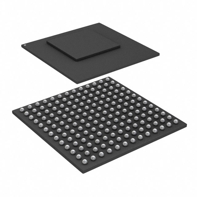


 工商网监
湘ICP备2023018690号
工商网监
湘ICP备2023018690号
