a
10-Bit, 400 MSPS
D/A Converters
AD9720/AD9721
lated bipolar process. The AD9720 is ECL compatible, and will
update up to 400 MSPS; the AD9721 is TTL compatible and
will update up to 100 MSPS.
Designed for direct digital synthesis (DDS), waveform reconstruction, and high resolution video applications, both devices
feature low glitch impulse of 1.5 pV-s and fast settling times of
4.5 ns to 1/2 LSB.
Both converters are characterized for dynamic performance, and
have excellent harmonic suppression and spectral purity in
waveform generation applications.
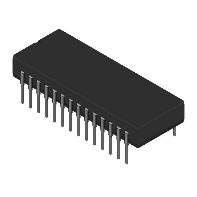
The units are available in 28-pin DIPs, LCCs and SOICs.
Industrial temperature range devices are packaged in plastic for
operation from –25°C to +25°C; extended temperature range
devices for operation from –55°C to +125°C are in hermetic
ceramic packages. Contact the factory for information about the
availability of MIL-STD-883 devices.
FEATURES
400 MSPS (ECL)/100 MSPS (TTL) Update Rate
Low Glitch Impulse: 1.5 pV-s
Fast Settling: 4.5 ns to 1/2 LSB
Low Power: 1.1 W
On-Board Quadrature Logic for DDS Applications
Differential Clock (ECL)
APPLICATIONS
Direct Digital Synthesis
Arbitrary Waveform Synthesis
Waveform Reconstruction
High Speed Imaging
OBS
OLE
The AD9720 and AD9721 D/A converters are 10-bit, high
speed digital-to-analog converters constructed in an oxide iso-
D 10
10
REGISTER
INVERTERS
D2
TTL
OR
ECL
DRIVE
LOGIC
DECODERS &
DRIVERS
D1
TE
FUNCTIONAL BLOCK DIAGRAM
SWITCH
NETWORK
GENERAL DESCRIPTION
ANALOG
RETURN
IOUT
IOUT
INVERT
CLOCK
REFERENCE
IN
CLOCK
+
R SET
REFERENCE
OUT
0.1µF
CONTROL
AMP OUT
CONTROL
AMP
INTERNAL
VOLTAGE
REFERENCE
–
CONTROL
AMP IN
DIGITAL
–V S
DIGITAL
+V S
BYP.
–5.2V
ANALOG
–V S
BYP.
+5V
BYP.
–5.2V
REV. A
Information furnished by Analog Devices is believed to be accurate and
reliable. However, no responsibility is assumed by Analog Devices for its
use, nor for any infringements of patents or other rights of third parties
which may result from its use. No license is granted by implication or
otherwise under any patent or patent rights of Analog Devices.
One Technology Way, P.O. Box 9106, Norwood, MA 02062-9106, U.S.A.
Tel: 617/329-4700
Fax: 617/326-8703
�AD9720/AD9721–SPECIFICATIONS
(–V = –5.2 V; +V = +5 V (AD9721 only); Reference Voltage = –1.25 V;
ELECTRICAL CHARACTERISTICS
Parameter (Conditions)
S
Test
AD9720BN/BR
Temp Level Min Typ Max
RESOLUTION
DC ACCURACY
Differential Nonlinearity
Integral Nonlinearity
(“Best Fit” Straight Line)
INITIAL OFFSET ERROR
Zero-Scale Offset Error
Full-Scale Gain Error 1
REFERENCE/CONTROL AMP
Internal Reference Voltage
Internal Reference Voltage Drift
Internal Reference Output Current
Amplifier Input Impedance
Amplifier Bandwidth
+25°C
Full
+25°C
Full
I
VI
I
VI
0.25
+25°C
Full
+25°C
Full
+25°C
I
VI
I
VI
V
16
20
2
+25°C
Full
Full
Full
+25°C
+25°C
I
VI
V
IV
V
V
0.5
+25°C
+25°C
+25°C
+25°C
+25°C
+25°C
+25°C
+25°C
+25°C
+25°C
+25°C
V
IV
V
V
V
V
V
V
V
V
V
Full
Full
Full
Full
+25°C
+25°C
Full
+25°C
Full
+25°C
+25°C
VI
VI
VI
VI
V
IV
IV
IV
IV
IV
IV
+25°C
+25°C
+25°C
+25°C
+25°C
V
V
V
V
V
75
66
70
55
70
+25°C
Full
+25°C
Full
+25°C
+25°C
I
VI
I
VI
V
V
210
DYNAMIC PERFORMANCE
Spurious-Free Dynamic Range (SFDR) 11
2.02 MHz; 100 MSPS; 2 MHz Span
25.01 MHz; 100 MSPS; 2 MHz Span
10.02 MHz; 250 MSPS; 5 MHz Span
62.54 MHz; 250 MSPS; 5 MHz Span
70 MHz; 220 MSPS; 10 MHz Span
POWER SUPPLY 12
Negative Supply Current (–5.2 V) 13
Positive Supply Current (+5.0 V)
Nominal Power Dissipation
Power Supply Rejection Ratio (PSRR) 14
0.6
60
75
15
15
16
20
2
0.7
1.0
1.5
1.5
2.0
0.25
60
75
15
15
16
20
2
–1.25
10
0.5
0.04
–1.15
–1.15
–1.35
–1.35
–1.15
–1.15
–1.25
1.2
0.85
0.85
20.48
+3
–1.5
210
6
100
4.5
4.5
1.5
1,000
675
470
3
0.4
0.85
0.85
N/A
N/A
1.1
50
–2–
–1.15
–1.15
V
V
µV/°C
µA
kΩ
MHz
+500
–50
kΩ
MHz
TE
20.48
+3
+3
210
6
100
4.5
4.5
1.5
1,000
675
470
2.0
3
0.5
1.25
0.85
0.85
218
14
1.2
50
290
300
30
30
mA
V
Ω
pF
MSPS
ns
ns
pV-s
V/µs
ps
ps
0.85
0.85
V
V
µA
µA
pF
ns
ns
ns
ns
ns
ns
75
66
N/A
N/A
N/A
dBc
dBc
dBc
dBc
dBc
0.8
400
700
1.0
1.2
2.0
2.3
1.0
1.1
75
66
N/A
N/A
N/A
280
290
–1.5
0.8
400
700
1.0
1.2
2.0
2.3
1.0
1.1
1.2
210
N/A
N/A
1.1
50
–1.35
–1.35
2.0
75
66
70
55
70
280
290
0.04
µA
µA
%
%
µA/°C
4.6
75
–1.6
50
2
1.0
1.2
1.6
2.8
1.1
1.4
60
75
15
15
4.6
75
–0.9
3
0.4
16
20
2
4.6
75
–1.5
50
2
1.0
1.2
1.6
2.8
1.1
1.4
60
75
15
15
50
1
–50
210
6
400
4.5
4.0
1.5
1,000
675
470
–1.0
LSB
LSB
LSB
LSB
50
1
–1.5
210
6
400
4.5
4.0
1.5
1,000
675
470
1.0
1.5
1.5
2.0
0.7
100
+500
20.48
+3
0.6
0.04
100
20.48
–1.5
0.75
1.0
1.0
1.5
Units
Bits
–1.25 –1.35
–1.35
100
+500
50
1
–50
4.6
75
AD9721TE/TQ
Min
Typ Max
10
OLE
OUTPUT PERFORMANCE
Full-Scale Output Current 2, 4
Output Compliance Range
Output Resistance
Output Capacitance
Output Update Rate
Voltage Settling Time (1/2 LSB) 5
Propagation Delay (t PD)6
Glitch Impulse 7
Output Slew Rate 8
Output Rise Time 8
Output Fall Time 8
Clock Pulse Width (Low)
Clock Pulse Width (High)
0 75
1.0
1.0
1.5
–1.15 –1.25 –1.35
–1.15
–1.35
100
–50
+500
50
1
+25°C V
+25°C V
Input Hold Time (t H)10
AD9721BN/BR
Min
Typ
Max
10
0.04
REFERENCE INPUT 2
Reference Input Impedance
Reference Multiplying Bandwidth 3
DIGITAL INPUTS
Logic “1” Voltage
Logic “0” Voltage
Logic “1” Current
Logic “0” Current
Input Capacitance
Input Setup Time (t S)9
AD9720TE/TQ
Min
Typ
Max
10
OBS
Offset Drift Coefficient
S
RSET = 1,960 V, unless otherwise noted)
3
0.5
1.25
218
14
1.2
50
290
300
30
30
mA
mA
mA
mA
W
µA/V
REV. A
�AD9720/AD9721
AD9720/AD9721
NOTES
11
Measured as error in ratio of full-scale current to current through R SET (640 µA nominal); ratio is nominally 32. DAC load is virtual ground.
12
Full-scale current variations among devices are higher when driving REFERENCE IN directly.
13
Frequency at which a 3 dB change in output of DAC is observed, R L = 50 Ω; 100 mV modulation at midscale.
14
Based on IFS = 32 (CONTROL AMP IN/R SET) when using internal control amplifier. DAC load is virtual ground.
15
Measured as voltage settling at midscale transition to ± 0.1%; RL = 50 Ω.
16
Measured from 50% point of rising edge of CLOCK signal to 1/2 LSB change in output signal.
17
Peak glitch impulse is measured as the largest area under a single positive or negative transient.
18
Measured with RL = 50 Ω and DAC operating in latched mode.
19
Data must remain stable for specified time prior to rising edge of CLOCK.
10
Data must remain stable for specified time after rising edge of CLOCK.
11
SFDR is defined as the difference in signal energy between the fundamental and worst case spurious frequencies in the output spectrum window, which is centered at
the fundamental frequency and covers the indicated span.
12
Supply voltages should remain stable within ± 5% for normal operation.
13
190 mA typ on Digital –V S, 30 mA typ on Analog –V S.
14
Measured at ± 5% of +VS (AD9721 only) and –V S (AD9720 or AD9721) using external reference.
Specifications subject to change without notice.
OBS
ABSOLUTE MAXIMUM RATINGS 1
EXPLANATION OF TEST LEVELS
Positive Supply Voltage (+VS) (AD9721 Only) . . . . . . . . +6 V
Negative Supply Voltage (–VS)
(AD9720 and AD9721) . . . . . . . . . . . . . . . . . . . . . . . . –7 V
Digital Input Voltages (D1–D10, CLOCK, CLOCK)
AD9720 . . . . . . . . . . . . . . . . . . . . . . . . . . . . . . . . 0 V to –VS
AD9721 . . . . . . . . . . . . . . . . . . . . . . . . . . . . . –0.5 V to +VS
Internal Reference Output Current . . . . . . . . . . . . . . . 500 µA
Control Amplifier Input Voltage Range . . . . . . . . . 0 V to –4 V
Control Amplifier Output Current . . . . . . . . . . . . . . . ± 2.5 mA
Reference Input Voltage Range (VREF) . . . . . . . . . . .0 V to –VS
Analog Output Current . . . . . . . . . . . . . . . . . . . . . . . . 30 mA
Operating Temperature Range
AD9720/AD9721BN/BR . . . . . . . . . . . . . . –25°C to +85°C
AD9720/AD9721TE/TQ . . . . . . . . . . . . . –55°C to +125°C
Maximum Junction Temperature2
AD9720/AD9721BN/BR . . . . . . . . . . . . . . . . . . . . +150°C
AD9720/AD9721TE/TQ . . . . . . . . . . . . . . . . . . . . +175°C
Lead Temperature (Soldering, 10 sec) . . . . . . . . . . . . +300°C
Storage Temperature Range . . . . . . . . . . . . –65°C to +150°C
Test Level
I – 100% production tested.
II – 100% production tested at +25°C, and sample tested at
specified temperatures.
III – Sample tested only.
IV – Parameter is guaranteed by design and characterization
testing.
V – Parameter is a typical value only.
VI – All devices are 100% tested at +25°C. 100% production
tested at temperature extremes for extended temperature
devices; sample tested at temperature extremes for commercial/industrial devices.
OLE
NOTES
1
Absolute maximum ratings are limiting values to be applied individually, and
beyond which the serviceability of the circuit may be impaired. Functional
operability is not necessarily implied. Exposure to absolute maximum rating
conditions for an extended period of time may affect device reliability.
2
Typical thermal impedances:
28-pin plastic DIP: θJA = 37°C/W, θJC = 10°C/W;
28-pin LCC:
θJA = 41°C/W, θJC = 13°C/W;
28-pin SOIC:
θJA = 46°C/W, θJC = 10°C/W;
Cerdip:
θJA = 35°C/W, θJC = 10°C/W.
Soldered to board; no air flow.
TE
DIE LAYOUT AND MECHANICAL INFORMATION
Die Dimensions . . . . . . . . . . . . . . . 199 3 165 3 15 (± 2) mils
Pad Dimensions . . . . . . . . . . . . . . . . . . . . . . . . . . . . 4 3 4 mils
Metalization . . . . . . . . . . . . . . . . . . . . . . . . . . . . . . Aluminum
Backing . . . . . . . . . . . . . . . . . . . . . . . . . . . . . . . . . . . . . None
Substrate Potential . . . . . . . . . . . . . . . . . . . . . . . . . . . . . . . –VS
Passivation . . . . . . . . . . . . . . . . . . . . . . . . . . . . . . . . . . Nitride
ORDERING GUIDE
Model
Temperature
Range
Package
Description
Package
Option
AD9720BN
AD9720BR
AD9720TE
AD9720TQ
–25°C to +85°C
–25°C to +85°C
–55°C to +125°C
–55°C to +125°C
28-Pin Plastic DIP
28-Pin SOIC
28-Pin LCC
28-Pin Cerdip
N-28
R-28
E-28A
Q-28
AD9721BN
AD9721BR
AD9721TE
AD9721TQ
–25°C to +85°C
–25°C to +85°C
–55°C to +125°C
–55°C to +125°C
28-Pin Plastic DIP
28-Pin SOIC
28-Pin LCC
28-Pin Cerdip
N-28
R-28
E-28A
Q-28
REV. A
–3–
�AD9720/AD9721
PIN DESCRIPTIONS
DIP
Pin # Name
Function
1
2-9
D1 (MSB)
D2–D9
10
D10 (LSB)
Most Significant Bit (MSB) of digital input word.
Eight of 10 digital input bits. Digital inputs are 10K ECL compatible for AD9720; TTL compatible
for AD9721. See coding table elsewhere.
Least Significant Bit (LSB) of digital input word.
Input Coding vs. Current Output
Input Code D1–D10
1111111111
0000000000
OBS
PIN CONFIGURATIONS
28
GROUND
2
27
DIGITAL –VS
D3
3
26 CONTROL AMP IN
D4
4
D5
5
D6
6
3
2
1
28
27
26
25 REFERENCE OUT
23
REFERENCE IN
22
ANALOG –VS
D7
7
D8
8
TOP VIEW
(Not to Scale)
21
IOUT
D9
9
20
IOUT
D10 (LSB)
10
19
ANALOG RETURN
CLOCK
11
18
GROUND
CLOCK (NC)
12
17
RSET
INVERT
13
16 DIGITAL –VS
15
GROUND
–4–
D5
5
25
D6
6
24
CONTROL AMP OUT
D7
7
23
REFERENCE IN
AD9720/AD9721
REFERENCE OUT
D8
8
LCC
22
ANALOG –VS
D9
9
TOP VIEW
(Not to Scale)
21
IOUT
D10 (LSB)
10
20
IOUT
CLOCK
11
19
ANALOG RETURN
12
13
14
15
16
17
18
RSET
24 CONTROL AMP OUT
GROUND
AD9720/
AD9721
DIP
DIGITAL –VS (+VS) 14
4
DIGITAL –VS
1
D2
CONTROL
AMP IN
D1 (MSB)
LCC Package
D1 (MSB)
DIP & SOIC Packages
GROUND
25
26
27
28
GROUND
24
DIGITAL –VS
21
22
23
TE
D3
20
D2
18
19
OLE
DIGITAL –VS (+VS)
14
15
16
17
Edge-triggered latch enable signal for on-board registers. 10K ECL compatible for AD9720. TTL
compatible for AD9721. Register loads data on rising edge of CLOCK signal; must be driven in conjunction with CLOCK.
CLOCK/NC
Complementary edge-triggered latch enable signal for on-board registers. 10K ECL compatible for
AD9720; not connected (NC) for AD9721.
INVERT
Normally connected to logic LOW; inverters are transparent in this mode. Logic High inverts the 9
LSBs (D2–D10) when the MSB is LOW. No internal pull-down resistor.
One of three digital supply pins; nominally –5.2 V for AD9720; +5 V for AD9721.
DIGITAL –VS/+VS
GROUND
Converter ground return.
One of three negative digital supply pins; nominally –5.2 V.
DIGITAL –VS
Connection for external resistance reference; nominally 1,960 Ω. Full-scale current out = 32 3
RSET
(CONTROL AMP IN/RSET) when using internal amplifier. DAC load is virtual ground.
GROUND
Converter ground return.
ANALOG RETURN
Analog current return. This point and the reference side of the DAC load resistors should be connected to the same potential (nominally ground).
Analog current output; full-scale output occurs with digital inputs at all “1.” With external load resisIOUT
tor, output voltage IOUT 3 (RLOAD || RINTERNAL). RINTERNAL is nominally 210 Ω.
Complementary analog current output; zero-scale output occurs with digital inputs at all “1.”
IOUT
Negative analog supply; nominally –5.2 V.
ANALOG –VS
REFERENCE IN
Normally connected to CONTROL AMP OUT (Pin 24). Direct line to DAC current source network.
Voltage changes (noise) at this point have a direct effect on the full-scale output current of DAC.
Full-scale current output = 32 3 (CONTROL AMP IN/RSET) when using internal amplifier. DAC
load is virtual ground.
CONTROL AMP OUT Normally connected to REFERENCE INPUT (Pin 23). Output of internal control amplifier, which
provides a reference for the current switch network.
REFERENCE OUT
Normally connected to CONTROL AMP IN (Pin 26). Internal voltage reference, nominally –1.25 V.
CONTROL AMP IN
Normally connected to REFERENCE OUT (Pin 25) if not connected to external reference.
One of three negative digital supply pins; nominally –5.2 V.
DIGITAL –VS
GROUND
Converter ground return.
D4
13
CLOCK
INVERT
12
IOUT (mA)
0
–20.48
CLOCK (NC)
11
IOUT (mA)
–20.48
0
REV. A
�AD9720/AD9721
CLOCK
CLOCK
CLOCK
CLOCK
ERROR
BAND
tS t H
DATA INPUTS
CODE 1
D 1 – D 10
VALID DATA
OUTPUT
ERROR
CODE 2
VALID DATA
t PD
OUTPUT
tS – INPUT SETUP TIME
CODE 2
tPD
t ST
CODE 1
t H – INPUT HOLD TIME
tST – OUTPUT SETTLING TIME
OBS
t PD – OUTPUT PROPAGATION DELAY
AD9720/AD9721 Timing Diagram
THEORY AND APPLICATIONS
The AD9720/AD9721 high speed digital-to-analog converters
utilize Most Significant Bit (MSB) decoding and segmentation
techniques to reduce glitch impulse and maintain 10-bit linearity without trimming.
When using the internal reference, REFERENCE OUT (Pin
25) should be connected to CONTROL AMP IN (Pin 26).
CONTROL AMP OUT (Pin 24) should be connected to REFERENCE IN (Pin 23). A 0.1 µF ceramic capacitor from Pin 23
to ANALOG –VS (Pin 22) improves settling by decoupling
switching noise from the current sink base line. A reference
current cell provides feedback to the control amp by sinking
current through RSET (Pin 17).
OLE
As shown in the functional block diagram, the design is based
on four main subsections: the Decoder/Driver circuits, the Edge
Triggered Data Register, the Switch Network, and the Control
Amplifier. An internal bandgap reference is also included to allow operation with a minimum of external components. The
block labeled “Inverters” is transparent in normal operation, but
can be used to minimize the external components requirements
in DDS applications using the AD9950, a 300 MSPS phase accumulator (see AD9950 data sheet).
Digital Inputs/Timing
The AD9720 employs single-ended ECL-compatible inputs for
data inputs D1–D10 and the differential clock signals CLOCK
and CLOCK. The internal ECL midpoint reference is designed
to match 10K ECL device thresholds. On the AD9721, a TTL
translator is added at each input and the clock becomes single
ended; with these exceptions, the AD9720 and AD9721 are
identical. (NOTE: Pin 14 is +VS on AD9721; –VS on AD9720.)
In the Decoder/Driver section, the four MSBs (D1–D4) are decoded to 15 “thermometer code” lines. An equalizing delay is
included for the six Least Significant Bits (LSBs) and the clock
signals. This delay minimizes data skew and data setup and hold
times at the register inputs.
TE
Full-scale output current is determined by CONTROL AMP IN
and RSET according to the equation:
IOUT (FS) = (CONTROL AMP IN/RSET) 3 32
The internal reference is nominally –1.25 V with a tolerance of
± 8% and typical drift over temperature of 100 ppm/°C. If
greater accuracy or better temperature stability is required, an
external reference can be utilized. The AD589 reference features
± 10 ppm/°C drift over temperatures from 0°C to +70°C.
Two modes of multiplying operation are possible with the
AD9720/AD9721. Signals with bandwidths up to 1 MHz and
input swings from –0.6 V to –1.2 V can be applied to the CONTROL AMP input as shown in Figure 1. Because the control
amplifier is internally compensated, the 0.1 µF capacitor discussed above can be reduced to maximize the multiplying bandwidth. However, it should be noted that settling time for
changes to the digital inputs will be degraded.
AD9720/AD9721
RSET
The on-board register is rising-edge-triggered and should be
used to synchronize data to the current switches by applying a
pulse with proper data set-up and hold times as shown in the
timing diagram.
17
RT
References
24
CONTROL
AMP OUT
23
REFERENCE
IN
0.1µF
As shown in the functional block diagram, the internal band-gap
reference, control amplifier, and reference input are pinned out
for maximum user flexibility when setting the reference.
REV. A
26 CONTROL
AMP IN
–0.6V TO –1.2V
400 kHz MAX
Although the AD9720/AD9721 chip is designed to provide isolation from digital inputs to the outputs, some coupling of digital transitions is inevitable, especially with TTL or CMOS
inputs applied to the AD9721. Digital feedthrough can be reduced by forming a low-pass filter using a resistor in series with
the capacitance of each digital input; this rolls off the slew rate
of the digital inputs.
RSET
ANALOG – VS
Figure 1. Low Frequency Multiplying Circuit
–5–
�AD9720/AD9721
The REFERENCE IN pin can also be driven directly for wider
bandwidth multiplying operation. The analog signal for this
mode of operation must have a signal swing in the range of
–3.3 V to –4.25 V. This can be implemented by capacitively
coupling into REFERENCE IN a signal with a dc bias of –3.3 V
(IOUT ~ 22.5 mA) to –4.25 V (IOUT ~ 3 mA), as shown in Figure
2, or by driving REFERENCE IN with a low impedance op
amp whose signal swing is limited to the stated range.
10k
+
10k
1/2
AD708
–
200
+
R1
1/2
AD708
–
100
R2
25
26
REF
OUT
CONTROL
AMP IN
AD9720/AD9721
IOUT
400
I FS
OBS
–
R FF
25
RL
I OUT
23
RFB
25
20
AD9720/
AD9721
REFERENCE
IN
IOS
V OUT
AD9617
±2.048 V
+
21
— –3.8V
–VS
Figure 3. I/V Conversion Using Current Feedback Amp
–VS
DDS Applications
The performance characteristics of the AD9720/AD9721 make
it ideally suited for direct digital synthesis (DDS) and other
waveform generation applications. Since the aliased distortion of
the DAC collects around the fundamental when generating frequencies which are nearly integer fractions of the clock rate,
these are often considered worst case conditions.
OLE
Figure 2. Wideband Multiplying Circuit
Outputs
The Switch Network provides complementary current outputs
IOUT and IOUT . The design of the AD9720/AD9721 is based on
statistical current source matching which provides 10-bit linearity without trim. Current is steered to either IOUT or IOUT in
proportion to the digital input code. The sum of the two currents is always equal to the full-scale output current minus one
LSB.
TE
Please contact the factory for information concerning the availability of an evaluation board or for additional characterization
data.
2 mV/DIVISION
The current output can be converted to a voltage by resistive
loading as shown in the block diagram. Both IOUT and IOUT
should be loaded equally for best overall performance. The voltage which is developed is the product of the output current and
the value of the load resistor.
An operational amplifier can also be used to perform the I to V
conversion of the DAC output. Figure 3 shows an example of a
circuit which uses the AD9617, a high speed, current feedback
amplifier. The resistor values in Figure 3 provide a 4.096 V
swing, centered at ground, at the output of the AD9617
amplifier.
SETTLING TIME ≈ 4.5ns
NET GLITCH = 1.34pV-s
PEAK GLITCH = 1.36pV-s
AD9720
I OUT
100 MHz
LPF
50Ω
TEST CIRCUIT
5 ns/DIVISION
Figure 4. AD9720 Glitch Impulse
–6–
REV. A
�AD9720/AD9721
0
0
0
AD9720 UPDATED
AT 220 MSPS
–10
AD9720 UPDATED
AT 250 MSPS
–10
–20
–20
–20
–30
–30
–30
dB –40
dB –40
dB –40
–50
–50
–50
–60
–60
–60
–70
–70
–70
–80
66
68
70
MHz
72
8
OBS
Figure 5. Typical Output Spectrum
0
AD9720 UPDATED
AT 100 MSPS
–10
–20
–30
dB –40
–50
–60
–70
–80
1.2
1.6
2.0
MHz
2.4
2.8
Figure 8. Typical Output Spectrum
TTL CLOCK
REFERENCE
GENERATOR
–80
–80
74
10
MHz
11
60
12
61
62
65
64
Figure 7. Typical Output Spectrum
0
OLE
AD9720 UPDATED
AT 100 MSPS
–10
–20
–20
–30
–30
dB –40
dB –40
–50
–50
–60
–60
–70
–70
AD9720 UPDATED
AT 250 MSPS
TE
–80
–80
24.2
24.6
25.0
MHz
25.4
25.8
Figure 9. Typical Output Spectrum
AD9955
100MHz
CMOS DDS
81
82
EXTERNAL
POWER
SUPPLY
+5V
–5.2V
AD9713B
OR
AD9721
DAC
50Ω
CABLE
AD9955 DDS EVALUATION BOARD
PROVIDED
IBM-COMPATIBLE PC
SPECTRUM ANALYZER
Figure 11. Direct Digital Synthesis System Diagram
–7–
83
MHz
84
85
Figure 10. Typical Output Spectrum
POWER
SUPPLY
INTERFACE
CLOCK
CIRCUIT
INTERFACE
LOGIC
REV. A
63
MHz
0
STANDARD PRINTER CABLE
SOFTWARE
PROVIDED
SOFTWARE
9
Figure 6. Typical Output Spectrum
–10
AD9720 UPDATED
AT 250 MSPS
–10
�AD9720/AD9721
OUTLINE DIMENSIONS
Dimensions shown in inches and (mm).
28-Pin Plastic DIP (Suffix N)
15
28
15
0.550 (13.97)
0.530 (13.46)
1
0.300 (7.60)
0.292 (7.40)
14
1.565 (39.70)
1.380 (35.10)
0.625 (15.8)
0.600 (15.24)
0.060 (1.52)
0.015 (0.38)
0.250 (6.35)
MAX
0.140
(3.56)
MIN
0.022 (0.558)
0.014 (0.356)
0.100 (2.54)
BSC
1
0.712 (18.08)
0.700 (17.78)
0.015 (0.381)
0.008 (0.204)
0.104 (2.65)
0.093 (2.35)
OBS
0.050 (1.27) BSC
28-Pin Leadless Chip Carrier (Suffix E)
0.100 (2.54)
0.064 (1.63)
0.055 (1.40)
0.045 (1.14)
1.91
0.75
REF
28
0.050 ± (1.27)
0.005 ± (0.13)
NO. 1 PIN INDEX
BOTTOM VIEW
0.040 x 45°
(1.02 x 45°)
REF 3 PLCS
0.419 (10.65)
0.319 (10.00)
14
0.70 (1.77)
MAX
1
C1636–24–3/92
28
28-Pin SOIC (Suffix R)
0.019 (0.49)
0.014 (0.35)
0.013 (0.32)
0.009 (0.23)
0.012 (0.3)
0.004 (0.1)
0.04 (1.02)
0.024 (0.61)
28-Pin Cerdip (Suffix Q)
OLE
1.490 (37.84) MAX
28
1
0.028 (0.71)
0.022 (0.56)
GLASS SEALANT
0.22
(5.59)
MAX
0.026 (0.660)
0.014 (0.356)
0.020 x 45°
(0.51 x 45°) REF
0.458 (11.63) 2
0.442 (11.23)
0.07 (1.78)
0.03 (0.76)
0.610 (15.49)
0.500 (12.70)
14
0.620 (15.74)
0.590 (14.93)
TE
0.018 (0.45)
0.008 (0.20)
0.125
(3.175)
MIN
15
0
PRINTED IN U.S.A.
NOTES
1. THIS DIMENSION CONTROLS THE OVERALL PACKAGE THICKNESS.
2. APPLIES TO ALL FOUR SIDES.
3. ALL TERMINALS ARE GOLD PLATED.
0.110 (2.79)
0.098 (2.45)
15
–8–
REV. A
�


 工商网监
湘ICP备2023018690号
工商网监
湘ICP备2023018690号
