HMC680LP4 / 680LP4E
v03.0609
BiCMOS MMIC 5-BIT DIGITAL
VARIABLE GAIN AMPLIFIER, 30 - 400 MHz
Typical Applications
Features
The HMC680LP4(E) is ideal for:
TTL/CMOS compatible parallel or latched
parallel control interface
• Cellular/3G Infrastructure
High Output IP3: +40 dBm (At all gain settings)
• WiBro / WiMAX / 4G
Low Noise Figure: 5 dB
• Microwave Radio & VSAT
Wide Gain Control Range: 23 dB
• Test Equipment and Sensors
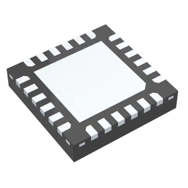
24 Lead 4x4 mm SMT Package: 16 mm2
• IF & RF Applications
Excellent State & Step Accuracy (±0.05 dB)
General Description
Functional Diagram
The HMC680LP4(E) is a digitally controlled variable
gain amplifier which operates from 30 to 400 MHz,
and can be programmed to provide -4 dB to +19 dB
of gain, in 1 dB steps. The HMC680LP4(E) delivers
noise figure of 5 dB in its maximum gain state, with
output IP3 of up to +40 dBm in any state. This high
linearity DVGA also provides a differential RF output
which can be used to interface directly with SAW
filters in Tx and Rx applications, and with digital to
analog converters in Rx chains. The HMC680LP4(E)
is housed in a RoHS compliant 4x4 mm QFN leadless
package, and is CMOS/ TTL compatible.
Variable gain amplifiers - digital - SMT
12
12 - 1
Electrical Specifications, TA = +25° C, 50 Ohm System, Vdd = +5V
Parameter
Min.
Frequency Range
Gain (Maximum Gain State)
Gain Control Range
17
Typ.
Max.
Units
30 - 400
MHz
19
23
dB
dB
Input Return Loss
12
dB
Output Return Loss
13
dB
Gain Accuracy: (Referenced to Maximum Gain State) All Gain States
± (0.15 + 3% of Gain Setting) Max.
Output Power for 1dB Compression
Output Third Order Intercept Point (Two-Tone Output Power= +5 dBm Each Tone) [1]
Output Second Order Intercept Point (Two-Tone Output Power= +5 dBm Each Tone) [1]
2nd Order
3rd Order
Harmonics
Step Accuracy (Referenced to Maximum Gain State)
Noise Figure (max gain state)
Switching Characteristics
Control Supply Current Idd
Amp Supply Current (RFOUTP)
Amp Supply Current (RFOUTN)
[1] Test frequency 50 MHz
tRise, tFall (10/90% RF)
tON, tOFF (50% CTL to 10/90% RF)
23
dB
25
40
65
dBm
dBm
dBm
70
75
dBc
dBc
±0.2
dB
5
dB
11
13
4
122
122
ns
ns
mA
mA
mA
5
135
135
Information furnished by Analog Devices is believed to be accurate and reliable. However, no
For price, 20
delivery,
and
to place
orders: Analog
For price,
delivery
and
to place
orders:
Microwave
Corporation,
Alpha
Road,
Chelmsford,
MADevices,
01824 Inc.,
responsibility
is assumed
by Analog
Devices
for its use,
nor for anyHittite
infringements
of patents or other
One Technology Way, P.O. Box 9106, Norwood, MA 02062-9106
rights of third parties that may result from its use. Specifications subject to change without notice. No
Phone: 978-250-3343
Fax: 978-250-3373
Order
at www.hittite.com
Phone: On-line
781-329-4700
• Order online at www.analog.com
license is granted by implication or otherwise under any patent or patent rights of Analog Devices.
Application
Support: Phone: 1-800-ANALOG-D
Trademarks and registered trademarks are
the property of their
respective owners.
Application
Support:
Phone: 978-250-3343
or apps@hittite.com
�HMC680LP4 / 680LP4E
v03.0609
BiCMOS MMIC 5-BIT DIGITAL
VARIABLE GAIN AMPLIFIER, 30 - 400 MHz
Normalized Attenuation
Maximum Gain vs. Frequency
(Only Major States are Shown)
25
NORMALIZED ATTENUATION (dB)
0
15
+25 C
+85 C
-40 C
10
5
0
-5
-10
8 dB
-15
16 dB
-20
-25
23 dB
-30
-35
0
0.1
0.2
0.3
0.4
0.5
0.6
0
0.1
FREQUENCY (GHz)
0.4
0.5
0.6
12
Output Return Loss
(Only Major States are Shown)
(Only Major States are Shown)
0
0
-5
I.L
-15
-20
-25
-30
Maximum Attenuation
-35
I.L
-5
-10
RETURN LOSS (dB)
RETURN LOSS (dB)
0.3
FREQUENCY (GHz)
Input Return Loss
-10
-15
Maximum Attenuation
-20
-25
-40
-30
0
0.1
0.2
0.3
0.4
0.5
0
0.6
0.1
FREQUENCY (GHz)
0.2
0.3
0.4
0.5
0.6
FREQUENCY (GHz)
Bit Error vs. Frequency
Bit Error vs. Attenuation State
(Only Major States are Shown)
2
5
1.5
4
Bit Error < 1dB, 400MHz And Below
3
1
1, 2, 4, 8, 16 dB
BIT ERROR (dB)
BIT ERROR (dB)
0.2
0.5
0
-0.5
-1
2
30MHz
1
0
-1
-2
-3
23 dB
-1.5
600MHz
-4
Bit Error > 1dB, 450MHz And Above
-5
-2
0
0.1
0.2
0.3
0.4
FREQUENCY (GHz)
0.5
0.6
0
4
8
12
16
20
24
ATTENUATION STATE (dB)
Information furnished by Analog Devices is believed to be accurate and reliable. However, no
For price, 20
delivery,
and
to place
orders: Analog
For price,
delivery
and
to place
orders:
Microwave
Corporation,
Alpha
Road,
Chelmsford,
MADevices,
01824 Inc.,
responsibility
is assumed
by Analog
Devices
for its use,
nor for anyHittite
infringements
of patents or other
One Technology Way, P.O. Box 9106, Norwood, MA 02062-9106
rights of third parties that may result from its use. Specifications subject to change without notice. No
Phone: 978-250-3343
Fax: 978-250-3373
Order
at www.hittite.com
Phone: On-line
781-329-4700
• Order online at www.analog.com
license is granted by implication or otherwise under any patent or patent rights of Analog Devices.
Application
Support: Phone: 1-800-ANALOG-D
Trademarks and registered trademarks are
the property of their
respective owners.
Application
Support:
Phone: 978-250-3343
or apps@hittite.com
variable gain amplifiers - digital - SMT
GAIN (dB)
20
12 - 2
�HMC680LP4 / 680LP4E
v03.0609
BiCMOS MMIC 5-BIT DIGITAL
VARIABLE GAIN AMPLIFIER, 30 - 400 MHz
Relative Phase vs. Frequency
Step Accuracy vs. Frequency
(Only Major States are Shown)
80
2
16 dB
1
RELATIVE PHASE (deg)
STEP ERROR (dB)
1.5
8 dB
0.5
0
-0.5
-1
1, 2, 4, 23 dB
0
1, 2, 4 dB
0
0.1
0.2
0.3
0.4
0.5
0.6
0
0.1
Output IP3 vs. Temperature
0.3
0.4
0.5
0.6
0.5
0.6
0.5
0.6
Output P1dB vs. Temperature
(+5 dBm Output Power Per Tone)
50
40
45
35
40
30
P1dB (dBm)
35
IP3 (dBm)
0.2
FREQUENCY (GHz)
FREQUENCY (GHz)
30
25
20
15
-40C
+25C
+85C
10
25
20
15
-40C
+25C
+85C
10
5
5
0
0
0
0.1
0.2
0.3
0.4
0.5
0
0.6
0.1
0.2
0.3
0.4
FREQUENCY (GHz)
FREQUENCY (GHz)
Output IP2 vs. Temperature
Noise Figure vs. Attenuation State
(+5 dBm Output Power Per Tone)
25
100
8dB
20
80
4dB
15
IP2 (dBm)
NOISE FIGURE (dB)
Variable gain amplifiers - digital - SMT
8 dB
20
-40
-2
12 - 3
16, 23 dB
40
-20
-1.5
12
60
2dB
1dB
10
5
60
40
-40C
+25C
+85C
20
I.L.
0
0
0
0.2
0.4
0.6
FREQUENCY (GHz)
0.8
1
0
0.1
0.2
0.3
0.4
FREQUENCY (GHz)
Information furnished by Analog Devices is believed to be accurate and reliable. However, no
For price, 20
delivery,
and
to place
orders: Analog
For price,
delivery
and
to place
orders:
Microwave
Corporation,
Alpha
Road,
Chelmsford,
MADevices,
01824 Inc.,
responsibility
is assumed
by Analog
Devices
for its use,
nor for anyHittite
infringements
of patents or other
One Technology Way, P.O. Box 9106, Norwood, MA 02062-9106
rights of third parties that may result from its use. Specifications subject to change without notice. No
Phone: 978-250-3343
Fax: 978-250-3373
Order
at www.hittite.com
Phone: On-line
781-329-4700
• Order online at www.analog.com
license is granted by implication or otherwise under any patent or patent rights of Analog Devices.
Application
Support: Phone: 1-800-ANALOG-D
Trademarks and registered trademarks are
the property of their
respective owners.
Application
Support:
Phone: 978-250-3343
or apps@hittite.com
�HMC680LP4 / 680LP4E
v03.0609
BiCMOS MMIC 5-BIT DIGITAL
VARIABLE GAIN AMPLIFIER, 30 - 400 MHz
Supply Current vs. Temperature
Harmonics vs. Frequency
280
0
2nd Harmonic
260
-40
-60
240
220
-80
-100
0
0.1
0.2
0.3
0.4
0.5
0.6
-40C
+25C
+85C
200
4.5
5
5.5
12
VOLTAGE (V)
FREQUENCY (GHz)
Absolute Maximum Ratings
Truth Table
RF Input Power
20 dBm
ATTENUATION (dB)
B4[1]
B3[1]
B2
B1
B0
RF Output Power
22 dBm
0
0
0
0
0
0
-0.5 to Vdd +0.5V
1
0
0
0
0
1
2
0
0
0
1
0
3
0
0
0
1
1
4
0
0
1
0
0
5
0
0
1
0
1
6
0
0
1
1
0
7
0
0
1
1
1
-65 to +150 °C
8
0
1
0
0
0
-40 to +85 °C
9
0
1
0
0
1
10
0
1
0
1
0
11
0
1
0
1
1
12
0
1
1
0
0
13
0
1
1
0
1
14
0
1
1
1
0
15
0
1
1
1
1
16
1
X
0
0
0
Digital Inputs (B0-B4, Latch Enable)
Bias Voltage (Vdd)
5.6 V
Channel Temperature
125 °C
Continuous Pdiss (T = 85 °C)
(derate 42 mW/°C above 85 °C)
1.7 W
Thermal Resistance
(channel to ground paddle)
Storage Temperature
Operating Temperature
24 °C/W
ELECTROSTATIC SENSITIVE DEVICE
OBSERVE HANDLING PRECAUTIONS
Amp Bias Voltage
Vdd RF (V)
Idd (Typ.) (mA)
17
1
X
0
0
1
5V
244
18
1
X
0
1
0
19
1
X
0
1
1
20
1
X
1
0
0
21
1
X
1
0
1
22
1
X
1
1
0
23
1
X
1
1
1
Control Voltage Table
State
Vdd = +3V
Vdd = +5V
Low
0 to 0.5V @


 工商网监
湘ICP备2023018690号
工商网监
湘ICP备2023018690号
