- Page
ANALOG DEVICES fAX-ON-DEMAND HOTLINE
,.
W
1~
ANALOG
DEVICES
12-BitSerialInput
Multiplying
CMOSD/AConverter
PM-7543
I
I
FEATURES
GENERAL DESCRIPTION
. Fast, Flexible Microprocessor Interface with Serial Data
Input
The PM-7543isa 12-bitresolution.multiplying, CMOS DtAconverter.
which features serial data input and current output. Serial data input
reduces pin count and allows the PM- 7543 to be placed in a smaller
package. saving PC board space. Improved analog parameters such
asdigitalchargeinjection, powersupply rejection. output capacitance,
feedthrough error. fast microprocessor interface. and improved ESD
protective circuitry make the PM- 7543 a superior pin-compatible
second-source to the industry standard AD7543.
.
.
..
Superior Accuracy
:t1/2 LSB INLMax
:t1 LSB Gain Error Max
Low 5ppml"C Max Tempco
. Improved ESD Resistance
Auto-Insertable DIP Package
. Surface Mount SOL Package
Superior Direct Replacement for AD7543
-40°C to +85°C for the Extended Industrial Temperature
Range
. Available In Die Form
The rising orfalling edge (user selected) ofthe strobe inputs are used
to clock serial data (present at the SRI pin) into the input shift register.
When the shift register's data has been updated. the new data word
is transferred to the DAC register with use of the LOAD inputs,
Continued
APPLICATIONS
Process Control and Industrial Automation
.
PIN CONNECTIONS
. ProgrammableAmplifiers
~ Digitally-Controlled Power Supplies, Attenuators, Filters
Instrumentation
.
5~~:j
.!?
.!? z a;
. Avionics
-
. Auto-Calibration Systems
ORDERING INFORMATIONt
TEMPERATURE
GAIN
ERROR
NONUNEARITY
COMMERCIAL
.i:2LSB
PM7543BO
PM7543BRC/883
PM7543FO
PM7S43FP
PM7543FS
PM7543FPC
Fordevicesprocessed
intotal
compliance
toMIL-STD-883.
add/883afler
number.
9111011111112'/13
PM7543EO
PM7543GP
:t1LSB
:l:1lSB
:l:1lSB
:l:1LSB
.i:2LSB
I
INDUSTRIAL
:l:1/2LSB
.i:2LSB
.
MILITARY.
:l:112LSB PM7543AO
.i:1LSB
:t2LSB
.i:2LSB
RANGE
EXTENDEDttf
Consultlactory
Burn.in is available on commercia!
and industrial temperature
CarDIP.
packages-
plastic DIP. and
part
lor /883 data sheet.
TO-can
1T For availability
and burn-ininformationon SO and PlCC
range
packages.
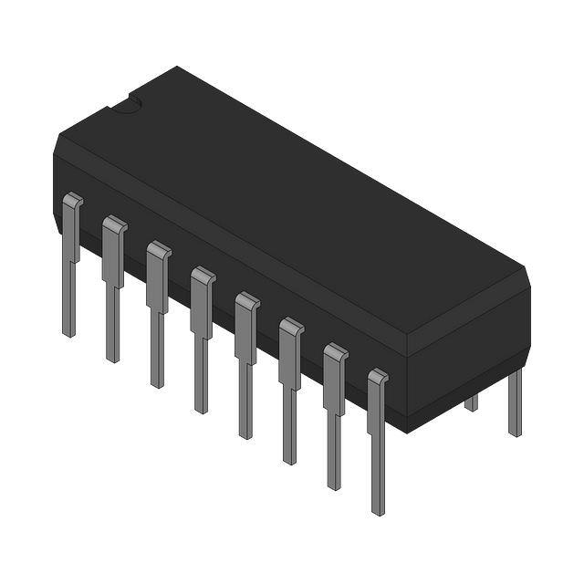
16-PIN EPOXY DIP
(P.Sufflx)
16-PIN CERDIP
(a-Suffix)
16-PINSOL
(S-Suffix)
ir
f/) &'!t.i
IZ !LIi!
...J!If/)
Of/)
2o-PIN Lce
(RC-Suffix)
20.PIN PLCe
(PC-Suffix)
parts in
contact
FUNCTIONAL BLOCK DIAGRAM
your local sales office.
ttt
CerDIP
ture
and
range
epoxy
01 -'lO.C
devices
are
available
in the
exlended
industrial
tempera-
PM-7543
to+8SoC.
CROSS REFERENCE
PMI
AD!
PM7543AO
PM7543AO
PM7543Ba
AD7543GTD
AD7543TD
AD7543SD
PM7543EO
PM7543EO
PM7543FO
AD7543G8D
AD75438D
AD7543AD
PM7543GP
PM7543GP
PM7543FP
PM7543FPC
AD7S43GKN
AD7543KN
AD7543JN
AD7S43JP
TEMPERATURE
RANGE
VAEf
-
IOU,,
15
lOUT>
3-AGNO
MIL
----.-
IND
CLR
- 13
LO'
LD~o-!
STBI- 4
7 -SRI
'4
-
VOD
12- DGND
COM
REV.D
Informationfurnishedby Analog Devices
isbelieved to be accurate and
reliable. However. no responsibility
is assumed by Analog Devices for its
use, nor for any infringements
of patents or other rights ofthird parties
which may result from its use. No license is granted by implication or
otherwise under any patent or patent rights of Analog Devices.
One Technology
Tel: 6171329-4700
Telex: 924491
Way, P.O. Box 9106, Norwood. MA 02062-9106. U.S.A
Fax: 6171326-8703
Twx; 710/394-6577
Cable: ANALOG NORWOODMASS
�ANALOG DEVICES fAX-ON-DEMAND HOTLINE
- Page
15
PM-7543
GENERAL DESCRIPTION Continued
Separate LOAD control inputs allow simultaneous output updating
of multiple DACs. An asynchronous CLEAR input resets the DAC
register without altering the data in the input register.
Operating Temperature
AOIBO Versions
EO/FO/FP/FPC/FS
,
Lead Temperature
ABSOLUTE MAXIMUM RATINGS (TA .. +25°C, unless
1-
60 see)
81"(Note1)
-65°C to +150°C
+300°C
81C
UNITS
94
12
.CIW
76
88
88
73
33
33
25
33
.CIW
.CIW
.CIW
.CIW
8.,. is specified for worst case mounting conditions. i.e., 8.,. is specified
dkvice in socket for CerDIP. P.DIP. andLCC pac:kages; £i,. is specified
for
for
device soldered to printed circuit board for SOL and PLCC ~ackages.
CAUTION:
+17V
:t25V
:t25V
VDD+ O.3V
1
.
Do not apply voltage higher than VCD or less than DGND potential on any
terminal
VDD + O.3V
-o.3V to VDO
,... -o.3V to VDD
Output Voltage (Pin 1. Pin 2)
(Soldering,
PACKAGE TYPE
16-PinHermetic DIP(0)
16-Pin
Plastic
DIP(P)
20.Contac:tLCC (RC)
2o-Pin
SOL (5)
2o-Contact
PLCC (PC)
NOTE:
otherwide noted.)
AGND to DGND
Digital Input Voltage Range """""""""""""""'"
DOCto +70°C
+150°C
m
CerDIP and epoxy devices are available in the extended industrial
temperature range of -40°C to +B5°C.
DGNDto AGND """""""""""""""""""""""""""
-55°C to + 125°C
-4aoC to +85°C
Versions
GP Version"""""""""""""""""""""""""'"
Junction Temperature
Storage Temperature
Improved linearity and gain error performance may permit reduced
circuit parts count through the elimination of trimming components.
Fast interface timing may reduce timing design considerations while
minimizing microprocessor wait states. The PM-7543 is available in
standard plast ic and CerDIP packages that are compatible with autoinsertion equipment. Foran even smalJerpackage, considerthe DAC8043, available in an a-pin mini-DIP.
Voo to DGND
VREF to DGND
VRFBto DGND
Range
except VREF (Pin 15) and RFB (Pin
16).
2. The digital control input are zener-protected; hoWever, permanent damage
mayoccuron unprotectedunits from high-energyelectrostatic;fields.
Keep
units in conductive foam at all times until ready to use.
3. Use proper antistatic handling procedures.
4. Absolute Maximum Ratings apply to both packaged device& and DICE.
Slresses above those listed under Absolute Maximum Ratings may cause
permanent damage to the device.
ELECTRICAL CHARACTERISTICS
at VOD" +5V; VREF" +1 OV;VOUT1.. VOUT2.. VAGND"VDGND= OV;T" .. Full Temperature
Range specified under Absolute Maximum Ratings, unless otherwise noted.
SYMBOL
PARAMETER
CONDITIONS
MIN
PM-7543
TYP
MAX
UNITS
STATIC ACCURACY
N
Resolution
Nonlinearity
INl
(Nole 1)
Differential Nonlinearity
(Note2)
DNl
12
-
PM-7S43A1EIG
-
PM-7S4381F
PM.7S43A!E
PM-754381F/G
T,.- +2S.C
-
PM.7543AiE
GainError
GFSE
(Note 3)
Power Supply
Rejection Ratio
-
-
TA=FuIlTemp.Range
All Grades
-
-
-
-
TCGFS
PSRR
-
PM-75438/F /G
Gain Tempco
(AGain/A Temp)
(Note 6)
-
-
AVCD - %5%
iO.OOO6
:t 1/2
:1:1
%112
:1:1
:1:1
%2
Bits
lSB
lS8
lSB
:1:2
:1:5
iO.OO2
ppml.
%/%
(t>.Gain/II VDC)
T" = +2S.C
Output leakage
(Notes 4.5)
Current
ILKG
T"
- Full Temp.
Range
PM-7543AIB
PM-7S43EIF/G
Zero Scale Error
(Notes B. 13)
Input Resistance
(Note 9)
'zSE
RIN
-
T" = +2S.C
T" FullTemp. Range
PM-7543AIB
PM-7543EIF/G
-
-
-
-
-
:1:0.002
-
:to.OS
-
7
VREF pin
-2-
:1:1
nA
:1:100
%10
:1:0_006
:to.01
iO.61
:to.06
11
15
L58
kG
REV.
D
�ANALOG DEVICES FAX-ON-DEMANDHOTLINE
- Page
16
PM- 7543
ELECTRICAL
CHARACTERISTICS
Range
under Absolute
specified
Maximum
at Voo
"" +5V;
Ratings,
VREF"" +10V;
unless
otherwise
VOUT1 "" VOUT2
:1:1
:t2
~
:1:1
VIL
%1% MAX
nA MAX
REFERENCE INPUT
................--
Input Resistance
7/15
k!l MINIMAX
DiGITAL INPUTS
Digital Input HIGH
VIH
2.4
VMIN
Digital Input lOW
VIL
0.8
VMAX
..........---..
Input Leakage
Current
IlL
:ti
VINKOVtoVoO
POWER SUPPLY
Supply Current
fLAMAX
--'00
Digital Inputs
Digital Inputs
K
V'H or V'l
=OV or V DO
2.0
0.1
mA MAX
...--
NOTE:
Electrical tests
:!.
...
z
c
-41.5
3
7
9
11
4
6
8
10
YRE' (YOLTS)
VOD (VOLTS'
-6-
REV.D
�ANALOGDEVICESfAX-ON-DEMAND
HOTLINE
- Page 20
PM-7543
SPECIFICATION
RESOLUTION
DEFINITIONS
v."
The resolutionof a DACis the number of states (2n) that the fullscale range (FSR) is divided (or resolved) into, where "n" is
equal to the number of bits.
SETTLING TIME
Time required for the analog output of the DAC to settle to within
1/2 LSB of its final value for a given digital input stimulus; i.e.
zero to full scale.
20...
200J!
5,
5.
10kl1
20kJJ
20kll
,I
Ratio of the DAC's external operational amplifier output voltage
to the V REFinput voltage when all digital inputs are HIGH.
5,.
BIT 1 IMSBI
ERROR
,
,
6
6
I
I
,
6
Error caused by capacitive coupling from VREF to output.
Feedthrough error limits are specified with all switches OFF.
BIT 2
(SWITCHES
i
1Okll
~
BIT 12 IlSBJ
DIGITAL INPUTS
SHOWN FOR DIGITAL INPUTS "HIGH")
Current appearing at loun when all digital inputs are LOW, or at
IOUT2terminal when all inputs are HIGH.
..ON
the feedback resistor and the R-2R ladder's terminating resIstor. The "Simplified DAC Circuit," Figure 1 ,shows the location of
these switches. These series switches are equivalently scaled
to two times switch 1 (MSB) and to switch 12 (LSB) to maintain
constant relative voltage drops with varying temperature. Dur-
GENERAL CIRCUIT INFORMATION
The PM-7543 is a 12-bit multiplying D/A converter with a very
low temperature coefficient, R-2R resistor ladder network, data
input and control logic, and two data registers. The digital circuitry forms an interface in which serial data can be loaded,
under microprocessor control, into a 12-bit shift register and
then transferred, in parallel, to the 12-bit DAC register.
An asynchronous CLEAR function allows resetting the DAC
register to a zero code (0000 0000 0000) without altering data
stored in the registers.
A simplified circuit of the PM-7543 DAC is shown in Figure 1. An
inverted R-2R ladder network consisting of silicon-chrome, thinfilm resistors, and twelve pairs of NMOS current-steering
switches. These switches steer binarily weighted currents into
either loun or IOUT2'Switching current to IOUT1
or IOUT2
yields a
constant current in each ladder leg, regardless of digital input
code. This constant current results in a constant input resis-
ing any testing of the resistor ladder or
coming inspection),
series switches.
RFEEDBACK
(such as in-
VDD must be present to turn "ON" these
ESO PROTECTION
The PM-7543 data inputs have been designed with ESD resistance incorporated through careful layout and the inclusion of
input protection circuitry.
Figure 2 shows the input protection diodes. High voltage static
charges applied to the digital inputs are shunted to the supply
and ground rails through forward biased diodes.
These protection diodes were designed to clamp the inputs well
below dangerous levels during static discharge conditions.
Von
at V AEF equal to R (typically
11kQ). The V REF input may be
driven by any reference voltage or current, AC or DC, that is
within the limits stated in the Absolute Maximum Ratings chart.
The twelve output current-steering switches are in series with
the R-2R resistor ladder, and therefore, can introduce bit errors.
It was essential to design these switches such that the switch
"ON" resistance be binarily scaled so that the voltage drop
across each switch remains constant. If, for example, switch 1
of Figure 1 was designed with an "ON" resistance of 10 ohms,
switch 2 for 20 ohms, etc., a constant 5mV drop would then be
maintained across each switch.
DTliTTl,CMOS
INPUTS
-=
FIGURE 2: Digital Input Protection
temperature range,
permanently "ON" MaS switches were included in series with
REV. D
PERMANENTLY
FIGURE 1: Simplified DAC Circuit
OUTPUT LEAKAGE CURRENT
across the full
IOU",
RHlDBACK
6
BIT3
.. THESESWITCHES
Capacitancefrom lOUT' to ground.
To further insure accuracy
lOUT>
I
r--,
~-"
OUTPUT CAPACITANCE
tance
20kl1
I
I
I
I
I
I
GAIN
FEEDTHROUGH
won
,oon
-7-
�ANALOG DEVICES fAX-ON-DEMAND HOTLINE
-
Page
21
PM-7543
I
FI,..OBACK
A _. 10kH
10"T1
t
'R"
- R-\Ok"
'om 2
v""
t
The gain and phase stability of the output amplifier, board layout, and power supply decoupling will all affect the dynamic
performance of the PM-7543. The use of a small compensation
capacitor may be required when high-speed operational amplifiers are used. It may be connected across the amplifiers feedback resistor to provide the necessary phase compensation to
critically damp the output.
The considerations when using high-speed amplifiers are:
1. Phase compensation (see Figures 7 and 8).
2. Power supply decoupling at the device socket and use of
proper grounding techniques.
APPLICATIONS INFORMATION
APPLICATIONTIPS
In most applications, linearity depends upon the potential of
FIGURE 3: PM-7543 Equivalent Circuit (All Inputs LOW)
IOUT1''OUT2'and AGND (pins 1,2, and 3) being exactly equal to
AFEEDSACk
each other. In most applications,the DACis connected to an
R" 10'H
'""
- R.,0kH
'OUT
VREF
external op amp with its noninverting input tied to ground (see
Figures 7 and 8). The amplifier selected should have a low input
bias current and low drift over temperature. The amplifier's input
offset voltage should be nulled to less than :t200~V (less than
10% of 1 LSB).
The operational amplifier's non inverting input should have a
minimum resistance connection to ground; the usual bias current compensation resistor should not be used. This resistor can
cause a variable offset voltage appearing as a varying output
1
t
'OUT>
t
error. Allgrounded pins should
tie to a single common ground
point, avoiding ground loops. The VOD power supply should
have a low noise level with no transients greater than + 17V.
FIGURE 4: PM- 7543 Equivalent Circuit (All Digital Inputs HIGH)
It is recommended that the digital inputs be taken to ground or
V DOvia a high value (1 Mn) resistor; this will prevent the accu-
EQUIVALENT CIRCUITANALVSIS
Figures 3 and 4 show equivalent circuits for the PM-7543's internal DAC with all bits LOW and HIGH, respectively. The reference current is switched to IOUT2when all data bits are LOW,
and to lOUT' when aU bits are HIGH. The ILEAKAGE
current
source is the combination of surface and junction leakages to
the substrate. The 1/4096 current source represents the constant 1-bit current drain through the ladder's terminating resistor.
mulation of static charge if the PC card is disconnected
system.
from the
Peak supply current flows as the digital inputs pass through the
transition
region
(see the Supply
Current
vs
logic
Input Voltage
graph under the Typical Performance Characteristics).
The
supply current decreases as the input voltage approaches the
supply rails (Voo or DGND), i.e. rapidly slewing logic signals that
settle very near the supply rails will minimize supply current.
Output capacitance is dependent upon the digital input code.
OUTPUT
This is because the gate capacitance of MOS transistors increases with applied gate voltage. This output capacitance varies between the low and high values.
AMPLIFIER
CONSIDERATIONS
When using high speed op amps, a small feedback capacitor
(typically 5-30pF) should be used across the amplifier to minimize overshoot and ringing, For low speed or static applications,
AC specifications of the amp1ifier are not very critical. In highspeed applications, slew rate, settling time, open-loop gain, and
gain/phase margin specifications of the amplifier should be se-
DYNAMIC PERFORMANCE
OUTPUT IMPEDANCE
The output resistance, as in the case of the output capacitance,
varies with the digital input code. This resistance, looking back
into the 'OUT1terminal, may be between 11kn (the feedback
resistor alone when all digital inputs are LOW) and 7.5kQ (the
feedback resistor in parallel with approximately 30kQ of the R2R ladder network resistance when any single bit logic is HIGH).
Static accuracy and dynamic performance will be affected by
these variations.
lected for the desired performance. It has already been noted
that an offset can be caused by including the usual bias current
compensation resistor in the amplifier's non inverting input terminal. This resistor should not be used. Instead, the amplifier
should have a bias current which is low over the temperature
range of interest.
-8-
REV. 0
�ANALOG DEVICES fAX-ON-DEMAND HOTLINE
- Page
22
PM-7543
..
R
v~~-~-
A
2R
an amplifier with inherently fow Vos' Amplifiers with sufficiently
low Vos include PMl's OP- 77, OP-97. OP-O7, OP-27 and OP-42INTERFACE LOGIC OPERATION
The microprocessor interface of the PM-7543 has been designed with multiple STROBE and LOAD inputs to maximize
interfacing options, Control signals decoding may be done onchip or with the use of external decoding circuitry (see Figure 11).
HC
2R
fA r
If'
Serial data can be clocked into the input register with STB 1.
STB2, or STB4. The strobe inputs are active on the rising edge.
STB3 may be used with a falling edge to clock-in data.
Holding any STROBE input at its selected
state (i.e. STB1.
FIGURE5: Simplified Circuit
STB2or STB4at logicHIGHor S"f'B3 at logicLOW) will act to
Static accuracy is affected by the variation in the DAC's output
resistance. This variation is best illustrated by using the circuit
of Figure 5 and the equation:
When a new data word has
prevent any further data input.
it is transferred
inputs.
INTERFACE INPUT DESCRIPTION
STB1 (Pin 4), STB2 (Pin 8), STB4 (Pin 11) - Input Register
Strobe. Inputs Active on Rising Edge. Selected to load serial
=2 Vas
= Vas (1 +!Qk!~
1okQ
)
data into input register. See Table 1 for details.
STB3 (Pin 10) -Input Register Strobe Input. Active on Failing Edge. Selected to load serial data into input register See
at code 0100 0000 0000,
VERR0R2
= Voo
10ka
1 + --30kn
(
Table 1 for details.
= 4/3 Voo
)
LD1 (Pin 5), LD2 (Pin 9)
-
Load DAC Register
Inputs.
Active
Low. Selected together to load contents of Input Register into
The error difference is 2/3 Vos'
DAC register.
Since one LSB has a weight (for VREF= +1OV)of 2.4mV for the PM7543. itis clearly important that Vas be minimized, either using the
amplifier's nullingpins, an external nullingnetwork, or by selection of
CLR (Pin 13)
SRI
BIT1
,H'.
"I
'STRO
BEIHPUTos><
os


 工商网监
湘ICP备2023018690号
工商网监
湘ICP备2023018690号
