Sample &
Buy
Product
Folder
Support &
Community
Tools &
Software
Technical
Documents
CSD86350Q5D
SLPS223F – MAY 2010 – REVISED OCTOBER 2016
CSD86350Q5D Synchronous Buck NexFET™ Power Block
1 Features
3 Description
•
•
•
•
•
•
•
•
•
•
•
The CSD86350Q5D NexFET™ power block is an
optimized design for synchronous buck applications
offering high-current, high-efficiency, and highfrequency capability in a small 5-mm × 6-mm outline.
Optimized for 5-V gate drive applications, this product
offers a flexible solution capable of offering a highdensity power supply when paired with any 5-V gate
drive from an external controller/driver.
Half-Bridge Power Block
90% System Efficiency at 25 A
Up to 40-A Operation
High-Frequency Operation (up to 1.5 MHz)
High-Density SON 5-mm × 6-mm Footprint
Optimized for 5-V Gate Drive
Low-Switching Losses
Ultra-Low Inductance Package
RoHS Compliant
Halogen Free
Lead-Free Terminal Plating
1
.
Top View
2 Applications
•
Synchronous Buck Converters
– High-Frequency Applications
– High-Current, Low-Duty Cycle Applications
Multiphase Synchronous Buck Converters
POL DC-DC Converters
IMVP, VRM, and VRD Applications
•
•
•
8
VSW
7
VSW
3
6
VSW
4
5
BG
VIN
1
VIN
2
TG
TGR
PGND
(Pin 9)
P0116-01
.
Device Information(1)
DEVICE
MEDIA
QTY
PACKAGE
SHIP
CSD86350Q5D
13-Inch Reel
2500
CSD86350Q5DT
7-Inch Reel
250
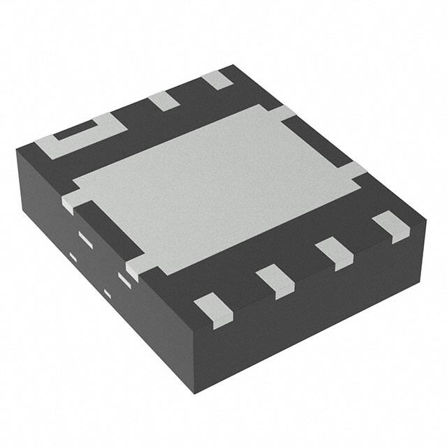
SON
5.00-mm × 6.00-mm
Plastic Package
Tape
and
Reel
(1) For all available packages, see the orderable addendum at
the end of the data sheet.
.
.
CSD86350Q5D
ENABLE
VIN
BST
DRVH
TG
Control
FET
TGR
VSW
ENABLE
PWM
LL
PWM
GND
DRVL
BG
VI
VO
Efficiency (%)
Driver IC
VDD
VDD
Typical Power Block Efficiency
and Power Loss
Sync
FET
PGND
100
6
90
5
VGS = 5V
VIN = 12V
VOUT = 1.3V
LOUT = 0.3,H
fSW = 500kHz
T A = 25 C
80
70
4
3
60
2
50
1
Power Loss (W)
Typical Circuit
S0474-01
40
0
5
10
15
Output Current (A)
20
0
25
G029
1
An IMPORTANT NOTICE at the end of this data sheet addresses availability, warranty, changes, use in safety-critical applications,
intellectual property matters and other important disclaimers. PRODUCTION DATA.
�CSD86350Q5D
SLPS223F – MAY 2010 – REVISED OCTOBER 2016
www.ti.com
Table of Contents
1
2
3
4
5
6
Features ..................................................................
Applications ...........................................................
Description .............................................................
Revision History.....................................................
Specifications.........................................................
1
1
1
2
4
5.1
5.2
5.3
5.4
5.5
5.6
5.7
4
4
4
4
5
6
8
Absolute Maximum Ratings ......................................
Recommended Operating Conditions.......................
Thermal Information ..................................................
Power Block Performance ........................................
Electrical Characteristics...........................................
Typical Power Block Device Characteristics.............
Typical Power Block MOSFET Characteristics.........
Application and Implementation ........................ 11
6.1 Application Information............................................ 11
7
Layout ................................................................... 16
7.1 Layout Guidelines ................................................... 16
7.2 Layout Example ...................................................... 17
8
Device and Documentation Support.................. 18
8.1
8.2
8.3
8.4
8.5
9
Documentation Support .......................................... 18
Receiving Notification of Documentation Updates.. 18
Community Resources............................................ 18
Trademarks ............................................................. 18
Glossary .................................................................. 18
Mechanical, Packaging, and Orderable
Information ........................................................... 19
9.1
9.2
9.3
9.4
Q5D Package Dimensions......................................
Land Pattern Recommendation ..............................
Stencil Recommendation ........................................
Q5D Tape and Reel Information .............................
19
20
20
21
4 Revision History
NOTE: Page numbers for previous revisions may differ from page numbers in the current version.
Changes from Revision E (October 2011) to Revision F
Page
•
Added small reel option .......................................................................................................................................................... 1
•
Added footnote for pulsed current rating ................................................................................................................................ 4
•
Changed Recommended PCB Design Overview section to Layout section ........................................................................ 16
•
Added Device and Documentation Support section............................................................................................................. 18
•
Changed MECHANICAL DATA section to Mechanical, Packaging, and Orderable Information section ............................ 19
Changes from Revision D (September 2011) to Revision E
•
Page
Changed "DIM a" Millimeter Max value From: 1.55 To: 1.5 and Inches Max value From: 0.061 To: 0.059........................ 19
Changes from Revision C (November 2010) to Revision D
Page
•
Replace RDS(on) with ZDS(on) ..................................................................................................................................................... 5
•
Added Equivalent System Performance section .................................................................................................................. 11
•
Added Electrical Performance bullet .................................................................................................................................... 16
Changes from Revision B (September 2010) to Revision C
•
Page
Added the Stencil Recommendation illustration ................................................................................................................... 20
Changes from Revision A (May 2010) to Revision B
Page
•
Updated Figure 6.................................................................................................................................................................... 6
•
Updated Figure 7.................................................................................................................................................................... 6
•
Updated Figure 8.................................................................................................................................................................... 6
•
Updated Figure 9.................................................................................................................................................................... 6
2
Submit Documentation Feedback
Copyright © 2010–2016, Texas Instruments Incorporated
Product Folder Links: CSD86350Q5D
�CSD86350Q5D
www.ti.com
SLPS223F – MAY 2010 – REVISED OCTOBER 2016
Changes from Original (May 2010) to Revision A
Page
•
Changed graph title From: TYPICAL EFFICIENCY vs POWER LOSS To: TYPICAL POWER BLOCK EFFICIENCY
and POWER LOSS ................................................................................................................................................................ 1
•
Updated the Land Pattern Recommendation illustration...................................................................................................... 20
Submit Documentation Feedback
Copyright © 2010–2016, Texas Instruments Incorporated
Product Folder Links: CSD86350Q5D
3
�CSD86350Q5D
SLPS223F – MAY 2010 – REVISED OCTOBER 2016
www.ti.com
5 Specifications
5.1 Absolute Maximum Ratings
TA = 25°C (unless otherwise noted) (1)
MIN
MAX
–0.8
25
TG to TGR
–8
10
BG to PGND
–8
10
VIN to PGND
Voltage
Pulsed current rating, IDM (2)
V
120
A
13
W
Power dissipation, PD
Avalanche energy, EAS
UNIT
Sync FET, ID = 100 A, L = 0.1 mH
500
Control FET, ID = 58 A, L = 0.1 mH
168
mJ
Operating junction, TJ
–55
150
°C
Storage temperature, TSTG
–55
150
°C
(1)
(2)
Stresses beyond those listed under Absolute Maximum Ratings may cause permanent damage to the device. These are stress ratings
only, and functional operation of the device at these or any other conditions beyond those indicated in the Recommended Operating
Conditions is not implied. Exposure to absolute-maximum-rated conditions for extended periods may affect device reliability.
Pulse duration ≤ 50 µs, duty cycle ≤ 1%.
5.2 Recommended Operating Conditions
TA = 25° (unless otherwise noted)
MIN
VGS
Gate drive voltage
VIN
Input supply voltage
fSW
Switching frequency
4.5
UNIT
8
V
22
CBST = 0.1 μF (min)
200
Operating current
TJ
MAX
Operating temperature
V
1500
kHz
40
A
125
°C
5.3 Thermal Information
TA = 25°C (unless otherwise stated)
THERMAL METRIC
RθJA
RθJC
(1)
(2)
MAX
UNIT
Junction-to-ambient thermal resistance (min Cu) (1) (2)
102
°C/W
Junction-to-ambient thermal resistance (max Cu) (1) (2)
50
°C/W
Junction-to-case thermal resistance (top of package) (2)
20
°C/W
2
°C/W
Junction-to-case thermal resistance (PGND pin)
2
MIN
TYP
(2)
(6.45-cm2)
2
Device mounted on FR4 material with 1-in
Cu.
RθJC is determined with the device mounted on a 1-in (6.45-cm2), 2 oz (0.071-mm) thick Cu pad on a 1.5-in × 1.5-in
(3.81-cm × 3.81-cm), 0.06-in (1.52-mm) thick FR4 board. RθJC is specified by design while RθJA is determined by the user’s board
design.
5.4 Power Block Performance
TA = 25° (unless otherwise noted)
PARAMETER
CONDITIONS
MIN
TYP
MAX
UNIT
PLOSS
Power loss (1)
VIN = 12 V, VGS = 5 V,
VOUT = 1.3 V, IOUT = 25 A,
fSW = 500 kHz,
LOUT = 0.3 µH, TJ = 25°C
2.8
W
IQVIN
VIN quiescent current
TG to TGR = 0 V
BG to PGND = 0 V
10
µA
(1)
4
Measurement made with six 10-µF (TDK C3216X5R1C106KT or equivalent) ceramic capacitors placed across VIN to PGND pins and
using a high-current 5-V driver IC.
Submit Documentation Feedback
Copyright © 2010–2016, Texas Instruments Incorporated
Product Folder Links: CSD86350Q5D
�CSD86350Q5D
www.ti.com
SLPS223F – MAY 2010 – REVISED OCTOBER 2016
5.5 Electrical Characteristics
TA = 25°C (unless otherwise stated)
PARAMETER
Q1 Control FET
TEST CONDITIONS
MIN
TYP
Q2 Sync FET
MAX
MIN
TYP
MAX
UNIT
STATIC CHARACTERISTICS
BVDSS
Drain-to-source voltage
VGS = 0 V, IDS = 250 μA
IDSS
Drain-to-source leakage current
VGS = 0 V, VDS = 20 V
25
IGSS
Gate-to-source leakage current
VDS = 0 V, VGS = +10 / –8 V
VGS(th)
Gate-to-source threshold voltage
VDS = VGS, IDS = 250 μA
ZDS(on)
Drain-to-source on impedance
VIN = 12 V, VDD = 5 V,
VOUT = 1.3 V, IOUT = 25 A,
fSW = 500 kHz, LOUT = 0.3 µH
gfs
Transconductance
VDS = 10 V, IDS = 20 A
25
V
1
100
0.9
1.4
2.1
0.9
1.1
1
μA
100
nA
1.6
V
5
1.1
mΩ
103
132
S
DYNAMIC CHARACTERISTICS
CISS
Input capacitance (1)
COSS
Output capacitance (1)
CRSS
Reverse transfer capacitance (1)
1440
1870
3080
4000
pF
645
840
1550
2015
pF
22
29
45
59
pF
VGS = 0 V, VDS = 12.5 V,
f = 1 MHz
(1)
RG
Series gate resistance
Qg
Gate charge total (4.5 V) (1)
Qgd
Gate charge – gate-to-drain
Qgs
Gate charge – gate-to-source
Qg(th)
Gate charge at Vth
QOSS
Output charge
td(on)
Turnon delay time
tr
Rise time
td(off)
Turnoff delay time
tf
Fall time
VDS = 12.5 V,
IDS = 20 A
VDS = 12 V, VGS = 0 V
VDS = 12.5 V, VGS = 4.5 V,
IDS = 20 A, RG = 2 Ω
1.4
2.8
1.4
2.8
Ω
8.2
10.7
19.4
25
nC
1
2.5
nC
3.2
5.1
nC
1.9
2.8
nC
9.9
28
nC
8
9
ns
21
23
ns
9
24
ns
2.3
21
ns
DIODE CHARACTERISTICS
VSD
Diode forward voltage
Qrr
Reverse recovery charge
trr
Reverse recovery time
(1)
IDS = 20 A, VGS = 0 V
0.85
Vdd = 12 V, IF = 20 A,
di/dt = 300 A/μs
16
1
0.77
40
1
nC
V
22
32
ns
Specified by design.
HD
LD
HD
LG
HG
HS
LS
86350 5x6 QFN TTA MIN Rev1
86350 5x6 QFN TTA MIN Rev1
Max RθJA = 50°C/W
when mounted on 1-in2
(6.45-cm2) of 2-oz
(0.071-mm) thick Cu.
LD
Max RθJA = 102°C/W
when mounted on
minimum pad area of
2-oz (0.071-mm) thick
Cu.
LG
HG
M0189-01
HS
LS
M0190-01
Submit Documentation Feedback
Copyright © 2010–2016, Texas Instruments Incorporated
Product Folder Links: CSD86350Q5D
5
�CSD86350Q5D
SLPS223F – MAY 2010 – REVISED OCTOBER 2016
www.ti.com
5.6 Typical Power Block Device Characteristics
TJ = 125°C, unless stated otherwise.
10
1.2
VIN = 12V
VGS = 5V
VOUT = 1.3V
fSW = 500kHz
LOUT = 0.3*H
Power Loss (W)
8
7
VIN = 12V
VGS = 5V
VOUT = 1.3V
fSW = 500kHz
LOUT = 0.31H
1.1
Power Loss, Normalized
9
6
5
4
3
1
0.9
0.8
0.7
2
0.6
1
0
0.5
0
5
10
15
20
25
Output Current (A)
30
35
40
50
45
45
40
40
35
35
30
25
20
400LFM
200LFM
100LFM
Nat Conv
VIN = 12V
VGS = 5V
VOUT = 1.3V
fSW = 500kHz
LOUT = 0.3*H
10
5
0
25
50
75
100
Junction Temperature ( C)
125
150
G002
Figure 2. Normalized Power Loss vs Temperature
50
Output Current (A)
Output Current (A)
Figure 1. Power Loss vs Output Current
50
15
25
G001
30
25
20
10
5
0
400LFM
200LFM
100LFM
Nat Conv
VIN = 12V
VGS = 5V
VOUT = 1.3V
fSW = 500kHz
LOUT = 0.3*H
15
0
0
10
20
30
40
50
60
Ambient Temperature ( C)
70
80
90
0
10
20
G003
Figure 3. Safe Operating Area – PCB Vertical Mount (1)
30
40
50
60
Ambient Temperature ( C)
70
80
90
G004
Figure 4. Safe Operating Area – PCB Horizontal Mount (1)
50
45
Output Current (A)
40
35
30
25
20
VIN = 12V
VGS = 5V
VOUT = 1.3V
fSW = 500kHz
LOUT = 0.3)H
15
10
5
0
0
20
40
60
80
100
Board Temperature ( C)
120
G005
Figure 5. Typical Safe Operating Area
(1)
6
140
(1)
The Typical Power Block System Characteristic curves are based on measurements made on a PCB design with dimensions of 4 in (W)
× 3.5 in (L) x 0.062 in (H) and 6 copper layers of 1-oz copper thickness. See Application and Implementation for detailed explanation.
Submit Documentation Feedback
Copyright © 2010–2016, Texas Instruments Incorporated
Product Folder Links: CSD86350Q5D
�CSD86350Q5D
www.ti.com
SLPS223F – MAY 2010 – REVISED OCTOBER 2016
Typical Power Block Device Characteristics (continued)
TJ = 125°C, unless stated otherwise.
1.5
10.5
1.4
5.2
1.1
2.6
1
0
0.9
*2.6
0.8
*5.2
0.7
*7.9
0.6
200
350
*10.5
500 650 800 950 1100 1250 1400 1550
Switching Frequency (kHz)
G006
1.3
1.6
1.5
VGS = 5V
VIN = 12V
LOUT = 0.3+H
fSW = 500kHz
IO = 40A
5.2
2.6
1
%2.6
0.8
%5.2
0.7
%7.8
0.6
2
!
1.4
10.4
1.3
7.8
1.2
5.2
1.1
2.6
4
6
8
10
12
14
Input Voltage (V)
16
18
20
%10.5
22
G007
Figure 7. Normalized Power Loss vs Input Voltage
"
13
0
0.9
18.2
15.6
7.8
1.1
20.8
SOA Temperature Adj ( C)
Power Loss, Normalized
1.7
10.5
1.2
Figure 6. Normalized Power Loss vs Switching Frequency
1.8
13.1
!#
( ) (
('* ) !(
( +, )
(
-*. ) ! /
) 0
!
#%
!
"
%
& "
$
&!
$2.6
#
&# %
0.8
$5.2
0.5 0.9 1.3 1.7 2.1 2.5 2.9 3.3 3.7 4.1 4.5 4.9 5.3
Output Voltage (V)
"
1
0
0.9
Figure 8. Normalized Power Loss vs Output Voltage
2
7.9
1.2
15.7
VGS = 5V
VOUT = 1.3V
LOUT = 0.3,H
fSW = 500kHz
IO = 40A
SOA Temperature Adj ( C)
1.6
13.1
0 1
1.3
15.7
* 0,
1.4
VIN = 12V
VGS = 5V
VOUT = 1.3V
LOUT = 0.32H
IO = 40A
Power Loss, Normalized
Power Loss, Normalized
1.5
SOA Temperature Adj ( C)
1.6
&
!
"
#
$
!
%
G008
'
%
Figure 9. Normalized Power Loss vs Output Inductance
Submit Documentation Feedback
Copyright © 2010–2016, Texas Instruments Incorporated
Product Folder Links: CSD86350Q5D
7
�CSD86350Q5D
SLPS223F – MAY 2010 – REVISED OCTOBER 2016
www.ti.com
5.7 Typical Power Block MOSFET Characteristics
TA = 25°C, unless stated otherwise.
8
Figure 10. Control MOSFET Saturation
Figure 11. Sync MOSFET Saturation
Figure 12. Control MOSFET Transfer
Figure 13. Sync MOSFET Transfer
Figure 14. Control MOSFET Gate Charge
Figure 15. Sync MOSFET Gate Charge
Submit Documentation Feedback
Copyright © 2010–2016, Texas Instruments Incorporated
Product Folder Links: CSD86350Q5D
�CSD86350Q5D
www.ti.com
SLPS223F – MAY 2010 – REVISED OCTOBER 2016
Typical Power Block MOSFET Characteristics (continued)
TA = 25°C, unless stated otherwise.
!"
!"
Figure 16. Control MOSFET Capacitance
!
"
Figure 17. Sync MOSFET Capacitance
#
!" #
Figure 18. Control MOSFET VGS(th)
Figure 19. Sync MOSFET VGS(th)
% $
"# $
&
% $
&
°#
"# $
"# $
$
°#
°#
"# $
!
Figure 20. Control MOSFET RDS(on) vs VGS
°#
!
Figure 21. Sync MOSFET RDS(on) vs VGS
Submit Documentation Feedback
Copyright © 2010–2016, Texas Instruments Incorporated
Product Folder Links: CSD86350Q5D
9
�CSD86350Q5D
SLPS223F – MAY 2010 – REVISED OCTOBER 2016
www.ti.com
Typical Power Block MOSFET Characteristics (continued)
TA = 25°C, unless stated otherwise.
"# $ %
&! $ &
#$ % &
'! % '
!
!
Figure 22. Control MOSFET Normalized RDS(on)
Figure 23. Sync MOSFET Normalized RDS(on)
Figure 24. Control MOSFET Body Diode
Figure 25. Sync MOSFET Body Diode
!
!
Figure 26. Control MOSFET Unclamped Inductive Switching
10
"
Figure 27. Sync MOSFET Unclamped Inductive Switching
Submit Documentation Feedback
Copyright © 2010–2016, Texas Instruments Incorporated
Product Folder Links: CSD86350Q5D
�CSD86350Q5D
www.ti.com
SLPS223F – MAY 2010 – REVISED OCTOBER 2016
6 Application and Implementation
NOTE
Information in the following applications sections is not part of the TI component
specification, and TI does not warrant its accuracy or completeness. TI’s customers are
responsible for determining suitability of components for their purposes. Customers should
validate and test their design implementation to confirm system functionality.
6.1 Application Information
6.1.1 Equivalent System Performance
Many of today’s high-performance computing systems require low-power consumption in an effort to reduce
system operating temperatures and improve overall system efficiency. This has created a major emphasis on
improving the conversion efficiency of today’s synchronous buck topology. In particular, there has been an
emphasis in improving the performance of the critical power semiconductor in the power stage of this application
(see Figure 28). As such, optimization of the power semiconductors in these applications, needs to go beyond
simply reducing RDS(ON).
Figure 28. Equivalent System Schematic
The CSD86350Q5D is part of TI’s power block product family which is a highly optimized product for use in a
synchronous buck topology requiring high-current, high-efficiency, and high-frequency. It incorporates TI’s latest
generation silicon which has been optimized for switching performance, as well as minimizing losses associated
with QGD, QGS, and QRR. Furthermore, TI’s patented packaging technology has minimized losses by nearly
eliminating parasitic elements between the control FET and sync FET connections (see Figure 29). A key
challenge solved by TI’s patented packaging technology is the system-level impact of Common Source
Inductance (CSI). CSI greatly impedes the switching characteristics of any MOSFET which in turn increases
switching losses and reduces system efficiency. As a result, the effects of CSI need to be considered during the
MOSFET selection process. In addition, standard MOSFET switching loss equations used to predict system
efficiency need to be modified in order to account for the effects of CSI. Further details behind the effects of CSI
and modification of switching loss equations are outlined in Power Loss Calculation With Common Source
Inductance Consideration for Synchronous Buck Converters (SLPA009).
Submit Documentation Feedback
Copyright © 2010–2016, Texas Instruments Incorporated
Product Folder Links: CSD86350Q5D
11
�CSD86350Q5D
SLPS223F – MAY 2010 – REVISED OCTOBER 2016
www.ti.com
Application Information (continued)
Figure 29. Elimination of Parasitic Inductances
The combination of TI’s latest generation silicon and optimized packaging technology has created a
benchmarking solution that outperforms industry standard MOSFET chipsets of similar RDS(ON) and MOSFET
chipsets with lower RDS(ON). Figure 30 and Figure 31 compare the efficiency and power loss performance of the
CSD86350Q5D versus industry standard MOSFET chipsets commonly used in this type of application. This
comparison purely focuses on the efficiency and generated loss of the power semiconductors only. The
performance of CSD86350Q5D clearly highlights the importance of considering the effective AC on-impedance
(ZDS(ON)) during the MOSFET selection process of any new design. Simply normalizing to traditional MOSFET
RDS(ON) specifications is not an indicator of the actual in-circuit performance when using TI’s power block
technology.
96
10
94
9
92
8
88
VGS = 5V
VIN = 12V
VOUT = 1.3V
LOUT = 0.3µH
fSW = 500kHz
TA = 25ºC
86
84
82
80
76
0
5
10
15
20
25
30
Output Current (A)
35
VGS = 5V
VIN = 12V
VOUT = 1.3V
LOUT = 0.3µH
fSW = 500kHz
TA = 25ºC
7
6
5
4
3
2
PowerBlock HS/LS RDS(ON) = 5mΩ/2mΩ
Discrete HS/LS RDS(ON) = 5mΩ/2mΩ
Discrete HS/LS RDS(ON) = 5mΩ/1.1mΩ
78
74
Power Loss (W)
Efficiency (%)
90
PowerBlock HS/LS RDS(ON) = 5mΩ/2mΩ
Discrete HS/LS RDS(ON) = 5mΩ/2mΩ
Discrete HS/LS RDS(ON) = 5mΩ/1.1mΩ
1
40
45
0
0
5
Figure 30. Efficiency
12
10
15
20
25
30
Output Current (A)
35
40
45
Figure 31. Power Loss
Submit Documentation Feedback
Copyright © 2010–2016, Texas Instruments Incorporated
Product Folder Links: CSD86350Q5D
�CSD86350Q5D
www.ti.com
SLPS223F – MAY 2010 – REVISED OCTOBER 2016
Application Information (continued)
Table 1 below compares the traditional DC measured RDS(ON) of CSD86350Q5D versus its ZDS(ON). This
comparison takes into account the improved efficiency associated with TI’s patented packaging technology. As
such, when comparing TI’s power block products to individually packaged discrete MOSFETs or dual MOSFETs
in a standard package, the in-circuit switching performance of the solution must be considered. In this example,
individually packaged discrete MOSFETs or dual MOSFETs in a standard package would need to have DC
measured RDS(ON) values that are equivalent to CSD86350Q5D’s ZDS(ON) value in order to have the same
efficiency performance at full load. Mid to light-load efficiency will still be lower with individually packaged discrete
MOSFETs or dual MOSFETs in a standard package.
Table 1. Comparison of RDS(ON) vs. ZDS(ON)
HS
PARAMETER
LS
TYP
MAX
TYP
MAX
Effective AC on-impedance (ZDS(ON)), VGS = 5 V
5
—
1.1
—
DC measured RDS(ON), VGS = 4.5 V
5
6.6
2
2.7
The CSD86350Q5D NexFET™ power block is an optimized design for synchronous buck applications using 5-V
gate drive. The control FET and sync FET silicon are parametrically tuned to yield the lowest power loss and
highest system efficiency. As a result, a new rating method is needed which is tailored towards a more systemscentric environment. System-level performance curves such as power loss, Safe Operating Area (SOA), and
normalized graphs allow engineers to predict the product performance in the actual application.
6.1.2 Power Loss Curves
MOSFET centric parameters such as RDS(ON) and Qgd are needed to estimate the loss generated by the devices.
In an effort to simplify the design process for engineers, Texas Instruments has provided measured power loss
performance curves. Figure 1 plots the power loss of the CSD86350Q5D as a function of load current. This curve
is measured by configuring and running the CSD86350Q5D as it would be in the final application (see
Figure 32).The measured power loss is the CSD86350Q5D loss and consists of both input conversion loss and
gate drive loss. Equation 1 is used to generate the power loss curve.
(VIN x IIN) + (VDD x IDD) – (VSW_AVG x IOUT) = Power Loss
(1)
The power loss curve in Figure 1 is measured at the maximum recommended junction temperatures of 125°C
under isothermal test conditions.
6.1.3 Safe Operating Area (SOA) Curves
The SOA curves in the CSD86350Q5D data sheet provides guidance on the temperature boundaries within an
operating system by incorporating the thermal resistance and system power loss. Figure 3 to Figure 5 outline the
temperature and airflow conditions required for a given load current. The area under the curve dictates the safe
operating area. All the curves are based on measurements made on a PCB design with dimensions of 4 in (W) ×
3.5 in (L) × 0.062 in (T) and 6 copper layers of 1-oz copper thickness.
6.1.4 Normalized Curves
The normalized curves in the CSD86350Q5D data sheet provides guidance on the power loss and SOA
adjustments based on their application specific needs. These curves show how the power loss and SOA
boundaries will adjust for a given set of systems conditions. The primary Y-axis is the normalized change in
power loss and the secondary Y-axis is the change in system temperature required in order to comply with the
SOA curve. The change in power loss is a multiplier for the power loss curve and the change in temperature is
subtracted from the SOA curve.
Submit Documentation Feedback
Copyright © 2010–2016, Texas Instruments Incorporated
Product Folder Links: CSD86350Q5D
13
�CSD86350Q5D
SLPS223F – MAY 2010 – REVISED OCTOBER 2016
Input Current (IIN)
Gate Drive
Current (IDD)
VDD
A
Gate Drive
Voltage (VDD) V
www.ti.com
VDD
ENABLE
VI
CSD86350Q5D
Driver IC
BST
DRVH
PWM
LL
GND
DRVL
PWM
A
VIN
TG
TGR
BG
V
Control
FET
Input Voltage (VIN)
Output Current (IOUT)
VO
VSW
A
Sync
FET
PGND
Averaging
Circuit
V
Averaged Switched
Node Voltage
(VSW_AVG)
S0475-01
Figure 32. Typical Application
6.1.5 Calculating Power Loss and SOA
The user can estimate product loss and SOA boundaries by arithmetic means (see Design Example). Though
the power loss and SOA curves in this data sheet are taken for a specific set of test conditions, the following
procedure will outline the steps the user should take to predict product performance for any set of system
conditions.
6.1.5.1 Design Example
Operating Conditions:
• Output Current = 25 A
• Input Voltage = 7 V
• Output Voltage = 1 V
• Switching Frequency = 800 kHz
• Inductor = 0.2 µH
6.1.5.2 Calculating Power Loss
•
•
•
•
•
•
Power loss at 25 A = 3.5 W (Figure 1)
Normalized power loss for input voltage ≈ 1.07 (Figure 7)
Normalized power loss for output voltage ≈ 0.95 (Figure 8)
Normalized power loss for switching frequency ≈ 1.11 (Figure 6)
Normalized power loss for output inductor ≈ 1.07 (Figure 9)
Final calculated power loss = 3.5 W × 1.07 × 0.95 × 1.11 × 1.07 ≈ 4.23 W
6.1.5.3 Calculating SOA Adjustments
•
•
•
•
•
SOA adjustment for input voltage ≈ 2°C (Figure 7)
SOA adjustment for output voltage ≈ –1.3°C (Figure 8)
SOA adjustment for switching frequency ≈ 2.8°C (Figure 6)
SOA adjustment for output inductor ≈ 1.6°C (Figure 9)
Final calculated SOA adjustment = 2 + (–1.3) + 2.8 + 1.6 ≈ 5.1°C
In the design example above, the estimated power loss of the CSD86350Q5D would increase to 4.23 W. In
addition, the maximum allowable board and/or ambient temperature would have to decrease by 5.1°C. Figure 33
graphically shows how the SOA curve would be adjusted accordingly.
1. Start by drawing a horizontal line from the application current to the SOA curve.
2. Draw a vertical line from the SOA curve intercept down to the board/ambient temperature.
14
Submit Documentation Feedback
Copyright © 2010–2016, Texas Instruments Incorporated
Product Folder Links: CSD86350Q5D
�CSD86350Q5D
www.ti.com
SLPS223F – MAY 2010 – REVISED OCTOBER 2016
3. Adjust the SOA board/ambient temperature by subtracting the temperature adjustment value.
In the design example, the SOA temperature adjustment yields a reduction in allowable board/ambient
temperature of 5.1°C. In the event the adjustment value is a negative number, subtracting the negative number
would yield an increase in allowable board/ambient temperature.
50
45
Output Current (A)
40
35
30
1
25
20
VIN = 12V
VGS = 5V
VOUT = 1.3V
fSW = 500kHz
LOUT = 0.3 mH
15
10
5
2
3
0
0
20
40
60
80
100
Board Temperature (°C)
120
140
G028
Figure 33. Power Block SOA
Submit Documentation Feedback
Copyright © 2010–2016, Texas Instruments Incorporated
Product Folder Links: CSD86350Q5D
15
�CSD86350Q5D
SLPS223F – MAY 2010 – REVISED OCTOBER 2016
www.ti.com
7 Layout
7.1 Layout Guidelines
There are two key system-level parameters that can be addressed with a proper PCB design: electrical and
thermal performance. Properly optimizing the PCB layout will yield maximum performance in both areas. A brief
description on how to address each parameter is provided.
7.1.1 Electrical Performance
The power block has the ability to switch voltages at rates greater than 10 kV/µs. Special care must be then
taken with the PCB layout design and placement of the input capacitors, driver IC, and output inductor.
• The placement of the input capacitors relative to the power block’s VIN and PGND pins should have the
highest priority during the component placement routine. It is critical to minimize these node lengths. As such,
ceramic input capacitors need to be placed as close as possible to the VIN and PGND pins (see Figure 34).
The example in Figure 34 uses 6 × 10-µF ceramic capacitors (TDK part C3216X5R1C106KT or equivalent).
Notice there are ceramic capacitors on both sides of the board with an appropriate amount of vias
interconnecting both layers. In terms of priority of placement next to the power block, C5, C7, C19, and C8
should follow in order.
• The driver IC should be placed relatively close to the power block gate pins. TG and BG should connect to the
outputs of the driver IC. The TGR pin serves as the return path of the high-side gate drive circuitry and should
be connected to the phase pin of the IC (sometimes called LX, LL, SW, PH, etc.). The bootstrap capacitor for
the driver IC will also connect to this pin.
• The switching node of the output inductor should be placed relatively close to the power block VSW pins.
Minimizing the node length between these two components will reduce the PCB conduction losses and
actually reduce the switching noise level. In the event the switch node waveform exhibits ringing that reaches
undesirable levels, the use of a boost resistor or RC snubber can be an effective way to easily reduce the
peak ring level. The recommended boost resistor value will range between 1 Ω to 4.7 Ω depending on the
output characteristics of driver IC used in conjunction with the power block. The RC snubber values can
range from 0.5 Ω to 2.2 Ω for the R and 330 pF to 2200 pF for the C. Please refer to Snubber Circuits:
Theory, Design and Application (SLUP100) for more details on how to properly tune the RC snubber values.
The RC snubber should be placed as close as possible to the VSW node and PGND see Figure 34. (1)
7.1.2 Thermal Performance
The power block has the ability to utilize the GND planes as the primary thermal path. As such, the use of
thermal vias is an effective way to pull away heat from the device and into the system board. Concerns of solder
voids and manufacturability problems can be addressed by the use of three basic tactics to minimize the amount
of solder attach that will wick down the via barrel:
• Intentionally space out the vias from each other to avoid a cluster of holes in a given area.
• Use the smallest drill size allowed in your design. The example in Figure 34 uses vias with a 10-mil drill hole
and a 16-mil capture pad.
• Tent the opposite side of the via with solder-mask.
In the end, the number and drill size of the thermal vias should align with the end user’s PCB design rules and
manufacturing capabilities.
(1)
16
Keong W. Kam, David Pommerenke, “EMI Analysis Methods for Synchronous Buck Converter EMI Root Cause Analysis”, University of
Missouri – Rolla
Submit Documentation Feedback
Copyright © 2010–2016, Texas Instruments Incorporated
Product Folder Links: CSD86350Q5D
�CSD86350Q5D
www.ti.com
SLPS223F – MAY 2010 – REVISED OCTOBER 2016
7.2 Layout Example
Input Capacitors
Input Capacitors
TGR
TG
VIN
PGND
Output Capacitors
Driver IC
Power Block
BG
V SW
VSW
V SW
RC Snubber
Power Block
Location on Top
Layer
Top Layer
Output Inductor
Bottom Layer
Figure 34. Recommended PCB Layout (Top Down View)
Submit Documentation Feedback
Copyright © 2010–2016, Texas Instruments Incorporated
Product Folder Links: CSD86350Q5D
17
�CSD86350Q5D
SLPS223F – MAY 2010 – REVISED OCTOBER 2016
www.ti.com
8 Device and Documentation Support
8.1 Documentation Support
8.1.1 Related Documentation
For related documentation see the following:
• Power Loss Calculation With Common Source Inductance Consideration for Synchronous Buck Converters
(SLPA009)
• Snubber Circuits: Theory, Design and Application (SLUP100)
8.2 Receiving Notification of Documentation Updates
To receive notification of documentation updates, navigate to the device product folder on ti.com. In the upper
right corner, click on Alert me to register and receive a weekly digest of any product information that has
changed. For change details, review the revision history included in any revised document.
8.3 Community Resources
The following links connect to TI community resources. Linked contents are provided "AS IS" by the respective
contributors. They do not constitute TI specifications and do not necessarily reflect TI's views; see TI's Terms of
Use.
TI E2E™ Online Community TI's Engineer-to-Engineer (E2E) Community. Created to foster collaboration
among engineers. At e2e.ti.com, you can ask questions, share knowledge, explore ideas and help
solve problems with fellow engineers.
Design Support TI's Design Support Quickly find helpful E2E forums along with design support tools and
contact information for technical support.
8.4 Trademarks
NexFET, E2E are trademarks of Texas Instruments.
All other trademarks are the property of their respective owners.
8.5 Glossary
SLYZ022 — TI Glossary.
This glossary lists and explains terms, acronyms, and definitions.
18
Submit Documentation Feedback
Copyright © 2010–2016, Texas Instruments Incorporated
Product Folder Links: CSD86350Q5D
�CSD86350Q5D
www.ti.com
SLPS223F – MAY 2010 – REVISED OCTOBER 2016
9 Mechanical, Packaging, and Orderable Information
The following pages include mechanical, packaging, and orderable information. This information is the most
current data available for the designated devices. This data is subject to change without notice and revision of
this document. For browser-based versions of this data sheet, refer to the left-hand navigation.
9.1 Q5D Package Dimensions
E2
K
d2
c1
4
5
4
q
L
d1
L
5
E1
6
3
6
3
b
9
D2
2
7
7
D1
2
E
e
8
1
8
1
d
d3
f
Top View
Bottom View
Side View
Pinout
Position
Exposed Tie Bar May Vary
q
a
c
E1
Front View
Pin 1
Designation
VIN
Pin 2
VIN
Pin 3
TG
Pin 4
TGR
Pin 5
BG
Pin 6
VSW
Pin 7
VSW
Pin 8
VSW
Pin 9
PGND
M0187-01
DIM
MILLIMETERS
INCHES
MIN
MAX
MIN
MAX
a
1.40
1.5
0.055
0.059
b
0.360
0.460
0.014
0.018
c
0.150
0.250
0.006
0.010
c1
0.150
0.250
0.006
0.010
d
1.630
1.730
0.064
0.068
d1
0.280
0.380
0.011
0.015
d2
0.200
0.300
0.008
0.012
d3
0.291
0.391
0.012
0.015
D1
4.900
5.100
0.193
0.201
D2
4.269
4.369
0.168
0.172
E
4.900
5.100
0.193
0.201
E1
5.900
6.100
0.232
0.240
E2
3.106
3.206
0.122
0.126
e
1.27 TYP
0.050 TYP
f
0.396
0.496
0.016
0.020
L
0.510
0.710
0.020
0.028
θ
0.00
—
—
—
K
0.812 TYP
0.032 TYP
Submit Documentation Feedback
Copyright © 2010–2016, Texas Instruments Incorporated
Product Folder Links: CSD86350Q5D
19
�CSD86350Q5D
SLPS223F – MAY 2010 – REVISED OCTOBER 2016
www.ti.com
9.2 Land Pattern Recommendation
3.480 (0.137)
0.530 (0.021)
0.415 (0.016)
0.345 (0.014)
0.650 (0.026)
5
4
0.650 (0.026)
4.460
(0.176)
0.620
(0.024)
0.620 (0.024)
4.460
(0.176)
1.270
(0.050)
1
1.920
(0.076)
8
0.850 (0.033)
0.400 (0.016)
0.850 (0.033)
6.240 (0.246)
M0188-01
NOTE: Dimensions are in mm (inches).
9.3 Stencil Recommendation
0.250 (0.010)
0.300 (0.012)
0.610 (0.024)
0.341 (0.013)
5
4
0.410 (0.016)
Stencil Opening
0.300 (0.012)
0.300 (0.012)
1.710
(0.067)
8
1
1.680
(0.066)
0.950 (0.037)
1.290 (0.051)
PCB Pattern
M0208-01
NOTE: Dimensions are in mm (inches).
.
For recommended circuit layout for PCB designs, see Reducing Ringing Through PCB Layout Techniques
(SLPA005).
20
Submit Documentation Feedback
Copyright © 2010–2016, Texas Instruments Incorporated
Product Folder Links: CSD86350Q5D
�CSD86350Q5D
www.ti.com
SLPS223F – MAY 2010 – REVISED OCTOBER 2016
9.4 Q5D Tape and Reel Information
4.00 ±0.10 (See Note 1)
K0
0.30 ±0.05
+0.10
2.00 ±0.05
Ø 1.50 –0.00
1.75 ±0.10
5.50 ±0.05
12.00 ±0.30
B0
R 0.20 MAX
A0
8.00 ±0.10
Ø 1.50 MIN
R 0.30 TYP
A0 = 5.30 ±0.10
B0 = 6.50 ±0.10
K0 = 1.90 ±0.10
M0191-01
NOTES: 1. 10-sprocket hole-pitch cumulative tolerance ±0.2.
2. Camber not to exceed 1 mm in 100 mm, noncumulative over 250 mm.
3. Material: black static-dissipative polystyrene.
4. All dimensions are in mm, unless otherwise specified.
5. Thickness: 0.30 ±0.05 mm.
6. MSL1 260°C (IR and convection) PbF reflow compatible.
Submit Documentation Feedback
Copyright © 2010–2016, Texas Instruments Incorporated
Product Folder Links: CSD86350Q5D
21
�PACKAGE MATERIALS INFORMATION
www.ti.com
18-Nov-2021
TAPE AND REEL INFORMATION
*All dimensions are nominal
Device
Package Package Pins
Type Drawing
SPQ
Reel
Reel
A0
Diameter Width (mm)
(mm) W1 (mm)
B0
(mm)
K0
(mm)
P1
(mm)
W
Pin1
(mm) Quadrant
CSD86350Q5D
LSONCLIP
DQY
8
2500
330.0
12.4
5.3
6.3
1.8
8.0
12.0
Q2
CSD86350Q5DT
LSONCLIP
DQY
8
250
180.0
12.4
5.3
6.3
1.8
8.0
12.0
Q2
Pack Materials-Page 1
�PACKAGE MATERIALS INFORMATION
www.ti.com
18-Nov-2021
*All dimensions are nominal
Device
Package Type
Package Drawing
Pins
SPQ
Length (mm)
Width (mm)
Height (mm)
CSD86350Q5D
LSON-CLIP
DQY
8
2500
367.0
367.0
35.0
CSD86350Q5DT
LSON-CLIP
DQY
8
250
182.0
182.0
20.0
Pack Materials-Page 2
�IMPORTANT NOTICE AND DISCLAIMER
TI PROVIDES TECHNICAL AND RELIABILITY DATA (INCLUDING DATA SHEETS), DESIGN RESOURCES (INCLUDING REFERENCE
DESIGNS), APPLICATION OR OTHER DESIGN ADVICE, WEB TOOLS, SAFETY INFORMATION, AND OTHER RESOURCES “AS IS”
AND WITH ALL FAULTS, AND DISCLAIMS ALL WARRANTIES, EXPRESS AND IMPLIED, INCLUDING WITHOUT LIMITATION ANY
IMPLIED WARRANTIES OF MERCHANTABILITY, FITNESS FOR A PARTICULAR PURPOSE OR NON-INFRINGEMENT OF THIRD
PARTY INTELLECTUAL PROPERTY RIGHTS.
These resources are intended for skilled developers designing with TI products. You are solely responsible for (1) selecting the appropriate
TI products for your application, (2) designing, validating and testing your application, and (3) ensuring your application meets applicable
standards, and any other safety, security, regulatory or other requirements.
These resources are subject to change without notice. TI grants you permission to use these resources only for development of an
application that uses the TI products described in the resource. Other reproduction and display of these resources is prohibited. No license
is granted to any other TI intellectual property right or to any third party intellectual property right. TI disclaims responsibility for, and you
will fully indemnify TI and its representatives against, any claims, damages, costs, losses, and liabilities arising out of your use of these
resources.
TI’s products are provided subject to TI’s Terms of Sale or other applicable terms available either on ti.com or provided in conjunction with
such TI products. TI’s provision of these resources does not expand or otherwise alter TI’s applicable warranties or warranty disclaimers for
TI products.
TI objects to and rejects any additional or different terms you may have proposed. IMPORTANT NOTICE
Mailing Address: Texas Instruments, Post Office Box 655303, Dallas, Texas 75265
Copyright © 2021, Texas Instruments Incorporated
�


 工商网监
湘ICP备2023018690号
工商网监
湘ICP备2023018690号
