Product
Folder
Order
Now
Support &
Community
Tools &
Software
Technical
Documents
Reference
Design
DRV8711
SLVSC40H – JUNE 2013 – REVISED MAY 2020
DRV8711 Stepper Motor Controller IC
1 Features
3 Description
•
The DRV8711 device is a stepper motor controller
that uses external N-channel MOSFETs to drive a
bipolar stepper motor or two brushed DC motors. A
microstepping indexer is integrated, which is capable
of step modes from full step to 1/256-step.
1
•
•
•
•
•
•
•
•
•
Pulse width modulation (PWM) microstepping
motor driver
– Built-In 1/256-Step microstepping indexer
– Drives external N-Channel MOSFETs
– Optional STEP/DIR pins
– Optional PWM control interface for DC motors
Flexible decay modes, including automatic mixed
decay mode
Stall detection with optional BEMF output
Highly configurable SPI serial interface
Internal reference and torque DAC
8-V to 52-V Operating supply voltage range
Scalable output current
Thermally enhanced surface-mount package
5-V Regulator capable of 10-mA load
Protection and diagnostic features
– Overcurrent protection (OCP)
– Overtemperature shutdown (OTS)
– Undervoltage lockout (UVLO)
– Individual fault condition indication bits
– Fault condition indication pin
A simple step/direction or PWM interface allows easy
interfacing to controller circuits. A SPI serial interface
is used to program the device operation. Output
current (torque), step mode, decay mode, and stall
detection functions are all programmable through a
SPI serial interface.
Internal shutdown functions are provided for
overcurrent protection, short-circuit protection,
undervoltage lockout, and overtemperature. Fault
conditions are indicated through a FAULTn pin, and
each fault condition is reported through a dedicated
bit through SPI.
The DRV8711 is packaged in a PowerPAD™ 38-pin
HTSSOP package with thermal pad (Eco-friendly:
RoHS and no Sb/Br).
Device Information(1)
2 Applications
•
•
•
•
An ultra-smooth motion profile can be achieved using
adaptive blanking time and various current decay
modes, including an auto-mixed decay mode. Motor
stall is reported with an optional back-EMF output.
PART NUMBER
Office Automation Machines
Factory Automation
Textile Machines
Robotics
DRV8711
PACKAGE
HTSSOP (38)
BODY SIZE (NOM)
9.70 mm × 4.40 mm
(1) For all available packages, see the orderable addendum at
the end of the data sheet.
Simplified Schematic
8.0 V to 52 V
Gate Drive
SPI
SLEEPn
nFAULT
Stepper
Motor
Pre-Driver
Sense
M
-
MCU
DIR
N-Channel
MOSFETs
DRV8711
+
STEP
+
-
1/256
µstep
1
An IMPORTANT NOTICE at the end of this data sheet addresses availability, warranty, changes, use in safety-critical applications,
intellectual property matters and other important disclaimers. PRODUCTION DATA.
�DRV8711
SLVSC40H – JUNE 2013 – REVISED MAY 2020
www.ti.com
Table of Contents
1
2
3
4
5
6
Features ..................................................................
Applications ...........................................................
Description .............................................................
Revision History.....................................................
Pin Configuration and Functions .........................
Specifications.........................................................
6.1
6.2
6.3
6.4
6.5
6.6
6.7
6.8
7
1
1
1
2
4
6
Absolute Maximum Ratings ...................................... 6
ESD Ratings ............................................................ 6
Recommended Operating Conditions....................... 6
Thermal Information .................................................. 6
Electrical Characteristics........................................... 7
SPI Timing Requirements ......................................... 8
Indexer Timing Requirements................................... 9
Typical Characteristics ............................................ 10
Detailed Description ............................................ 11
7.1
7.2
7.3
7.4
Overview .................................................................
Functional Block Diagram .......................................
Feature Description.................................................
Device Functional Modes........................................
11
12
13
26
7.5 Programming .......................................................... 27
7.6 Register Maps ........................................................ 27
8
Application and Implementation ........................ 32
8.1 Application Information............................................ 32
8.2 Typical Application ................................................. 32
9
Power Supply Recommendations...................... 40
9.1 Bulk Capacitance .................................................... 40
10 Layout................................................................... 41
10.1 Layout Guidelines ................................................. 41
10.2 Layout Example .................................................... 42
11 Device and Documentation Support ................. 43
11.1
11.2
11.3
11.4
11.5
11.6
Documentation Support ........................................
Receiving Notification of Documentation Updates
Community Resources..........................................
Trademarks ...........................................................
Electrostatic Discharge Caution ............................
Glossary ................................................................
43
43
43
43
43
43
12 Mechanical, Packaging, and Orderable
Information ........................................................... 43
4 Revision History
NOTE: Page numbers for previous revisions may differ from page numbers in the current version.
Changes from Revision G (May 2017) to Revision H
Page
•
Added content to Overcurrent Protection (OCP).................................................................................................................. 25
•
Added items to the Table 5 table.......................................................................................................................................... 33
•
Added Calculate Current Regulation section........................................................................................................................ 35
Changes from Revision F (July 2016) to Revision G
Page
•
Changed the description of the SCS pin in the Pin Functions table ...................................................................................... 4
•
Changed the maximum voltages for the charge pump voltage, high-side gate drive pin voltage, and phase node pin
voltage in the Absolute Maximum Ratings table .................................................................................................................... 6
•
Changed the OTS bit description in the STATUS register .................................................................................................. 30
•
Clarified UVLO bit operation when device is sleep mode .................................................................................................... 31
Changes from Revision E (March 2015) to Revision F
Page
•
Clarified that the SMPLTH bit 10 is a write-only bit in the TORQUE register ..................................................................... 23
•
Changed the default values for the OCPTH, OCPDEG, IDRIVEN, and IDRIVEP bits in the DRIVE register .................... 30
•
Added the Receiving Notification of Documentation Updates and Community Resources sections .................................. 43
Changes from Revision D (January 2014) to Revision E
•
2
Page
Added ESD Ratings table, Feature Description section, Device Functional Modes, Application and Implementation
section, Power Supply Recommendations section, Layout section, Device and Documentation Support section, and
Mechanical, Packaging, and Orderable Information section ................................................................................................. 1
Submit Documentation Feedback
Copyright © 2013–2020, Texas Instruments Incorporated
Product Folder Links: DRV8711
�DRV8711
www.ti.com
SLVSC40H – JUNE 2013 – REVISED MAY 2020
Changes from Revision C (December 2013) to Revision D
•
Page
Changed STATUS Register bit descriptions 3 through 5 ..................................................................................................... 30
Submit Documentation Feedback
Copyright © 2013–2020, Texas Instruments Incorporated
Product Folder Links: DRV8711
3
�DRV8711
SLVSC40H – JUNE 2013 – REVISED MAY 2020
www.ti.com
5 Pin Configuration and Functions
DCP PowerPAD™ Package
38-Pin HTSSOP
Top View
CP1
CP2
VCP
VM
GND
V5
VINT
SLEEPn
RESET
STEP / AIN1
DIR / AIN2
BIN1
BIN2
SCLK
SDATI
SCS
SDATO
FAULTn
STALLn / BEMFVn
1
2
3
38
37
36
4
5
35
34
6
7
33
32
31
8
9
10
11
30
GND
(PPAD)
29
28
12
27
13
26
14
25
15
24
16
23
17
22
18
21
19
20
GND
AOUT1
A1HS
A1LS
AISENP
AISENN
A2LS
A2HS
AOUT2
GND
BOUT1
B1HS
B1LS
BISENP
BISENN
B2LS
B2HS
BOUT2
BEMF
Pin Functions
PIN
NAME
NO.
I/O (1)
DESCRIPTION
EXTERNAL COMPONENTS OR CONNECTIONS
POWER AND GROUND
5, 29,
38,
PPAD
—
Device ground
All pins must be connected to ground
VM
4
—
Bridge A power supply
Connect to motor supply voltage. Bypass to GND with a 0.01-μF
ceramic capacitor plus a 100-μF electrolytic capacitor.
VINT
7
—
Internal logic supply voltage
Logic supply voltage. Bypass to GND with a 1-μF 6.3-V X7R ceramic
capacitor.
V5
6
O
5-V regulator output
5-V linear regulator output. Bypass to GND with a 0.1-μF 10-V X7R
ceramic capacitor.
CP1
1
IO
Charge pump flying capacitor
CP2
2
IO
Charge pump flying capacitor
Connect a 0.1-μF X7R capacitor between CP1 and CP2. Voltage
rating must be greater than applied VM voltage.
VCP
3
IO
High-side gate drive voltage
Connect a 1-μF 16-V X7R ceramic capacitor to VM
SLEEPn
8
I
Sleep mode input
Logic high to enable device, logic low to enter low-power sleep mode
STEP/AIN1
10
I
Step input/Bridge A IN1
Indexer mode: Rising edge causes the indexer to move one step.
External PWM mode: controls bridge A OUT1 Internal pulldown.
DIR/AIN2
11
I
Direction input/Bridge A IN2
Indexer mode: Level sets the direction of stepping.
External PWM mode: controls bridge A OUT2 Internal pulldown.
BIN1
12
I
Bridge B IN1
Indexer mode: No function
External PWM mode: controls bridge B OUT1 Internal pulldown.
BIN2
13
I
Bridge B IN2
Indexer mode: No function
External PWM mode: controls bridge B OUT2 Internal pulldown.
RESET
9
I
Reset input
Active-high reset input initializes all internal logic and disables the Hbridge outputs. Internal pulldown.
GND
CONTROL
SERIAL INTERFACE
SCS
16
I
Serial chip select input
Active high to enable serial data transfer. Active low to complete the
transaction. Internal pulldown.
SCLK
14
I
Serial clock input
Rising edge clocks data into part for write operations. Falling edge
clocks data out of part for read operations. Internal pulldown.
(1)
4
Directions: I = input, O = output, OZ = 3-state output, OD = open-drain output, IO = input/output
Submit Documentation Feedback
Copyright © 2013–2020, Texas Instruments Incorporated
Product Folder Links: DRV8711
�DRV8711
www.ti.com
SLVSC40H – JUNE 2013 – REVISED MAY 2020
Pin Functions (continued)
PIN
NAME
NO.
I/O (1)
SDATI
15
I
SDATO
17
STALLn/
BEMFVn
DESCRIPTION
EXTERNAL COMPONENTS OR CONNECTIONS
Serial data input
Serial data input from controller. Internal pulldown.
OD
Serial data output
Serial data output to controller. Open-drain output requires external
pullup.
19
OD
Stall/Back EMF valid
Internal stall detect mode: logic low when motor stall detected.
External stall detect mode: Active low when valid back EMF
measurement is ready.
Open-drain output requires external pullup.
FAULTn
18
OD
Fault
Logic low when in fault condition. Open-drain output requires external
pullup.
Faults: OCP, PDF, OTS, UVLO
BEMF
20
O
Back EMF
Analog output voltage represents motor back EMF. Place a 1-nF lowleakage capacitor to ground on this pin.
A1HS
36
O
Bridge A out 1 HS gate
Connect to gate of HS FET for bridge A out 1
AOUT1
37
I
Bridge A output 1
Connect to output node of external FETs of bridge A out 1
A1LS
35
O
Bridge A out 1 LS gate
Connect to gate of LS FET for bridge A out 1
A2HS
31
O
Bridge A out 2 HS gate
Connect to gate of HS FET for bridge A out 2
AOUT2
30
I
Bridge A output 2
Connect to output node of external FETs of bridge A out 2
A2LS
32
O
Bridge A out 2 LS gate
Connect to gate of LS FET for bridge A out 2
AISENP
34
I
Bridge A Isense + in
Connect to current sense resistor for bridge A
AISENN
33
I
Bridge A Isense – in
Connect to ground at current sense resistor for bridge A
B1HS
27
O
Bridge B out 1 HS gate
Connect to gate of HS FET for bridge B out 1
BOUT1
28
I
Bridge B output 1
Connect to output node of external FETs of bridge B out 1
B1LS
26
O
Bridge B out 1 LS gate
Connect to gate of LS FET for bridge B out 1
B2HS
22
O
Bridge B out 2 HS gate
Connect to gate of HS FET for bridge B out 2
BOUT2
21
I
Bridge B output 2
Connect to output node of external FETs of bridge B out 2
B2LS
23
O
Bridge B out 2 LS gate
Connect to gate of LS FET for bridge B out 2
BISENP
25
I
Bridge B Isense + in
Connect to current sense resistor for bridge B
BISENN
24
I
Bridge B Isense – in
Connect to ground at current sense resistor for bridge B
STATUS
OUTPUTS
Submit Documentation Feedback
Copyright © 2013–2020, Texas Instruments Incorporated
Product Folder Links: DRV8711
5
�DRV8711
SLVSC40H – JUNE 2013 – REVISED MAY 2020
www.ti.com
6 Specifications
6.1 Absolute Maximum Ratings
over operating free-air temperature range (unless otherwise noted) (1) (2) (3)
MIN
MAX
UNIT
Power supply voltage
–0.6
60
V
Charge pump voltage (CP2, VCP)
–0.6
VM + 12
V
Charge pump voltage (CP1)
–0.6
VM + 0.6
V
5-V regulator voltage (V5)
–0.6
5.5
V
Internal regulator voltage (VINT)
–0.6
2
V
Digital pin voltage (SLEEPn, RESET, STEP/AIN1, DIR/AIN2, BIN1, BIN2, SCS, SCLK, SDATI,
SDATO, FAULTn, STALLn/BEMFVn)
–0.6
5.5
V
High-side gate drive pin voltage (A1HS, A2HS, B1HS, B2HS)
–0.6
VM + 12
V
Low-side gate drive pin voltage (A1LS, A2LS, B1LS, B2LS)
–0.6
12
V
Phase node pin voltage (AOUT1, AOUT2, BOUT1, BOUT2)
–0.6
VM + 0.6
V
ISENSEx pin voltage (AISENP, AISENN, BISENP, BISENN)
–0.7
0.7
V
BEMF pin voltage (BEMF)
–0.6
5.5
V
Operating virtual junction temperature, TJ
–40
150
°C
Storage temperature, Tstg
–60
150
°C
(1)
(2)
(3)
Stresses beyond those listed under Absolute Maximum Ratings may cause permanent damage to the device. These are stress ratings
only, which do not imply functional operation of the device at these or any other conditions beyond those indicated under Recommended
Operating Conditions. Exposure to absolute-maximum-rated conditions for extended periods may affect device reliability.
All voltage values are with respect to network ground terminal.
Power dissipation and thermal limits must be observed.
6.2 ESD Ratings
VALUE
Electrostatic
discharge
V(ESD)
(1)
(2)
Human body model (HBM), per ANSI/ESDA/JEDEC JS-001 (1)
±4000
Charged device model (CDM), per JEDEC specification JESD22-C101 (2)
±1500
UNIT
V
JEDEC document JEP155 states that 500-V HBM allows safe manufacturing with a standard ESD control process.
JEDEC document JEP157 states that 250-V CDM allows safe manufacturing with a standard ESD control process.
6.3 Recommended Operating Conditions
over operating free-air temperature range (unless otherwise noted)
MIN
VM
Motor power supply voltage
IVS
V5 external load current
TA
Operating ambient temperature
NOM
MAX
UNIT
8
52
V
0
10
mA
-40
85
°C
6.4 Thermal Information
DRV8711
THERMAL METRIC (1)
DCP (HTSSOP)
UNIT
38 PINS
RθJA
Junction-to-ambient thermal resistance
32.7
°C/W
RθJC(top)
Junction-to-case (top) thermal resistance
17.2
°C/W
RθJB
Junction-to-board thermal resistance
14.3
°C/W
ψJT
Junction-to-top characterization parameter
0.5
°C/W
ψJB
Junction-to-board characterization parameter
14.1
°C/W
RθJC(bot)
Junction-to-case (bottom) thermal resistance
0.9
°C/W
(1)
6
For more information about traditional and new thermal metrics, see the Semiconductor and IC Package Thermal Metrics application
report.
Submit Documentation Feedback
Copyright © 2013–2020, Texas Instruments Incorporated
Product Folder Links: DRV8711
�DRV8711
www.ti.com
SLVSC40H – JUNE 2013 – REVISED MAY 2020
6.5 Electrical Characteristics
over operating free-air temperature range (unless otherwise noted)
PARAMETER
TEST CONDITIONS
MIN
TYP
MAX
UNIT
POWER SUPPLIES
IVM
VM operating supply current
VM = 24 V
17
20
mA
IVMQ
VM sleep mode supply current
VM = 24 V, SLEEPn = 0, TA = 25°C
65
98
μA
VM rising
7.1
8
VM falling
6.3
VUVLO
VM undervoltage lockout voltage
V
INTERNAL LINEAR REGULATORS
V5
V5 output voltage
VM ≥ 12 V, IOUT = 1 mA – 10 mA
4.8
5
5.2
V
VINT
VINT voltage
No external load – reference only
1.7
1.8
1.9
V
0.8
V
LOGIC-LEVEL INPUTS
VIL
Input low voltage
VIH
Input high voltage
VHYS
Input hysteresis voltage
IIL
Input low current
VIN = 0 V
–5
IIH
Input high current
VIN = 5 V
30
1.5
V
300
50
mV
5
μA
70
μA
SDATAO, STALLn, FAULTn OUTPUTS (OPEN-DRAIN OUTPUTS)
VOL
Output low voltage
IO = 5 mA
IOH
Output high leakage current
VO = 3.3 V
0.5
V
1
µA
MOSFET DRIVERS
VOUTH
High-side gate drive output voltage
VM = 24 V, IO = 100 μA
VM+10
V
VOUTL
Low-side gate drive output voltage
VM = 24 V, IO = 100 μA
10
V
tDEAD
Output dead time digital delay (dead
time is enforced in analog circuits)
IOUTH
IOUTl
tDRIVE
tDRIVE
Peak output current gate drive
(source)
Peak output current gate drive (sink)
Peak current drive time (source)
Peak current drive time (sink)
DTIME = 00
400
DTIME = 01
450
DTIME = 10
650
DTIME = 11
850
IDRIVEP = 00
50
IDRIVEP = 01
100
IDRIVEP = 10
150
IDRIVEP = 11
200
IDRIVEN = 00
100
IDRIVEN = 01
150
IDRIVEN = 10
200
IDRIVEN = 11
400
TDRIVEP = 00
250
TDRIVEP = 01
500
TDRIVEP = 10
1000
TDRIVEP = 11
2000
TDRIVEN = 00
250
TDRIVEN = 01
500
TDRIVEN = 10
1000
TDRIVEN = 11
2000
ns
mA
mA
ns
ns
MOTOR DRIVER
tOFF
PWM off time adjustment range
Set by TOFF register
0.5
128
μs
tBLANK
Current sense blanking time
Set by TBLANK register
0.5
5.12
μs
Submit Documentation Feedback
Copyright © 2013–2020, Texas Instruments Incorporated
Product Folder Links: DRV8711
7
�DRV8711
SLVSC40H – JUNE 2013 – REVISED MAY 2020
www.ti.com
Electrical Characteristics (continued)
over operating free-air temperature range (unless otherwise noted)
PARAMETER
TEST CONDITIONS
MIN
TYP
MAX
OCPTH = 00
160
250
320
OCPTH = 01
380
500
580
OCPTH = 10
620
750
850
OCPTH = 11
840
1000
1200
Die temperature
150
160
180
UNIT
PROTECTION CIRCUITS
VOCP
Overcurrent protection trip level
(Voltage drop across external FET)
tTSD
Thermal shutdown temperature (1)
tHYS
Thermal shutdown hysteresis
mV
°C
20
°C
CURRENT SENSE AMPLIFIERS
AV
Gain
ISGAIN = 00
5
ISGAIN = 01
10
ISGAIN = 10
20
ISGAIN = 11
tSET
Settling time (to ±1%)
VOFS
Offset voltage
VIN
Input differential voltage range
V/V
40
ISGAIN = 00, ΔVIN = 400 mV
150
ISGAIN = 01, ΔVIN = 200 mV
300
ISGAIN = 10, ΔVIN = 100 mV
600
ISGAIN = 11, ΔVIN = 50 mV
1.2
ISGAIN = 00, input shorted
–600
ns
µs
4
mV
600
mV
CURRENT CONTROL DACs
Resolution
256
Full-scale step response
VREF
(1)
10% to 90%
Full-scale (reference) voltage
2.50
2.75
steps
5
µs
3
V
Not tested in production; ensured by design.
6.6 SPI Timing Requirements
over operating free-air temperature range (unless otherwise noted) (see Figure 1)
NO.
8
MIN
NOM MAX UNIT
1
tCYC
Clock cycle time
250
ns
2
tCLKH
Clock high time
25
ns
3
tCLKL
Clock low time
25
ns
4
tSU(SDATI)
Setup time, SDATI to SCLK
5
ns
5
tH(SDATI)
Hold time, SDATI to SCLK
1
ns
6
tSU(SCS)
Setup time, SCS to SCLK
5
ns
7
tH(SCS)
Hold time, SCS to SCLK
1
ns
8
tL(SCS)
Inactive time, SCS (between writes and reads)
9
tD(SDATO)
Delay time, SCLK to SDATO (during read)
tSLEEP
Wake time (SLEEPn inactive to high-side gate drive enabled)
tRESET
Delay from power up or RESETn high until serial interface functional
Submit Documentation Feedback
100
ns
10
ns
1
ms
10
μs
Copyright © 2013–2020, Texas Instruments Incorporated
Product Folder Links: DRV8711
�DRV8711
www.ti.com
SLVSC40H – JUNE 2013 – REVISED MAY 2020
6.7 Indexer Timing Requirements
over operating free-air temperature range (unless otherwise noted) (see Figure 2)
NO.
MIN
NOM MAX UNIT
1
fSTEP
Step frequency
2
tWH(STEP)
Pulse duration, STEP high
1.9
250
3
tWL(STEP)
Pulse duration, STEP low
1.9
μs
4
tSU(STEP)
Setup time, command to STEP rising
200
ns
5
tH(STEP)
Hold time, command to STEP rising
200
ns
7
6
kHz
μs
8
SCS
1
SCLK
2
3
SDATI
X
X
4
5
9
SDATO
valid
SDATO
Figure 1. SPI Timing
1
2
3
STEP
DIR, MODE
4
5
Figure 2. Indexer Timing
Submit Documentation Feedback
Copyright © 2013–2020, Texas Instruments Incorporated
Product Folder Links: DRV8711
9
�DRV8711
SLVSC40H – JUNE 2013 – REVISED MAY 2020
www.ti.com
6.8 Typical Characteristics
17.5
240
±40ƒC
25°C
85°C
200
17.0
IVMQ (µA)
IVM (mA)
160
16.5
16.0
120
80
±40ƒC
15.5
40
25°C
85°C
15.0
8
12
16
20
24
28
32
36
40
44
48
VVM (V)
0
52
8
12
16
28
32
36
40
44
48
52
C006
Figure 4. Sleep Current
12
5.5
11
5.4
5.3
10
5.2
9
V5 No Load
RDS(ON) HS + LS) (mŸ)
24
VVM (V)
Figure 3. Operating Current
8
7
5.1
5.0
4.9
4.8
6
±40ƒC
4.6
85°C
4
8
12
16
20
24
28
32
36
40
Temperature (ƒC)
44
48
±40ƒC
25°C
4.7
25°C
5
85°C
4.5
52
8
C007
Figure 5. VCP Minus VM
10
20
C005
12
16
20
24
28
32
36
Temperature (ƒC)
40
44
48
52
C008
Figure 6. V5 No Load
Submit Documentation Feedback
Copyright © 2013–2020, Texas Instruments Incorporated
Product Folder Links: DRV8711
�DRV8711
www.ti.com
SLVSC40H – JUNE 2013 – REVISED MAY 2020
7 Detailed Description
7.1 Overview
The DRV8711 device is a stepper motor controller that uses external N-channel MOSFETs to drive a bipolar
stepper motor or two brushed DC motors. A microstepping indexer is integrated, which is capable of step modes
from full step to 1/256-step.
An ultra-smooth motion profile can be achieved using adaptive blanking time, adjustable decay times, and
various current decay modes, including an auto-mixed decay mode. When microstepping, motor stall can be
reported with an optional back-EMF output.
A simple step/direction or PWM interface allows easy interfacing to controller circuits. A SPI serial interface is
used to program the device operation. Output current (torque), step mode, decay mode, and stall detection
functions are all programmable through a SPI serial interface.
Internal shutdown functions are provided for overcurrent protection, short-circuit protection, undervoltage lockout,
and overtemperature. Fault conditions are indicated through a FAULTn pin, and each fault condition is reported
through a dedicated bit through SPI.
Submit Documentation Feedback
Copyright © 2013–2020, Texas Instruments Incorporated
Product Folder Links: DRV8711
11
�DRV8711
SLVSC40H – JUNE 2013 – REVISED MAY 2020
www.ti.com
7.2 Functional Block Diagram
VM
0.1µF
+
1µF
0.01µF
100µF
CP2
CP1
VM
VCP
VM
5V OUT
VM
Charge
Pump
V5
Gate
Drive
&
OCP
Regs
VINT
A1LS
PWM
logic
1µ F
RESET
UVLO
PUC
VM
DCM
Step
Motor
AOUT2
A2LS
+
Comp
+
-
DIR/AIN2
AISENP
ISEN
amp
-
STEP/AIN1
A2HS
Gate
Drive
&
OCP
OverTemp
SLEEPn
VM
AOUT1
+
0.1µF
A1HS
HS Gate Drive
AISENN
+
Comp
-
BIN1
SIN
DAC
BIN2
VM
X
B1HS
Gate
Drive
&
OCP
Torque
DAC
SCS
BOUT1
B1LS
Logic
PWM
logic
SCLK
SDATI
B2HS
Gate
Drive
&
OCP
Reference
SDATO
VM
DCM
BOUT2
B2LS
+
Comp
+
BISENP
ISEN
amp
-
+
-
-
FAULTn
BISENN
+
Comp
SIN
DAC
STALLn / BEMFVn
X
Torque
DAC
Stall detect
BEMF
1nF
GND
Copyright © 2017, Texas Instruments Incorporated
12
Submit Documentation Feedback
Copyright © 2013–2020, Texas Instruments Incorporated
Product Folder Links: DRV8711
�DRV8711
www.ti.com
SLVSC40H – JUNE 2013 – REVISED MAY 2020
7.3 Feature Description
Table 1 lists the critical components for the device.
Table 1. Critical Components
PIN
NAME
4
VM
COMPONENT
100-µF electrolytic rated for VM voltage to GND 0.01-µF ceramic rated for VM voltage to GND
3
VCP
1-µF ceramic X7R rated 16 V to VCP
1, 2
CP1, CP2
6
V5
7
VINT
1-µF ceramic X7R rated 6.3 V to GND
17
SDATO
Requires external pullup to logic supply
18
FAULTn
Requires external pullup to logic supply
19
STALLn/BEMFVn
Requires external pullup to logic supply
20
BEMF
0.1-µF rated for VM + 12 V between these pins
0.1-µF ceramic X7R rated 6.3 V to GND
1-nF low-leakage capacitor to GND
7.3.1 PWM Motor Drivers
The DRV8711 contains two H-bridge motor predrivers with current control PWM circuitry. More detailed
descriptions of the subblocks are described in the following sections.
7.3.2 Direct PWM Input Mode
Direct PWM mode is selected by setting the PWMMODE bit in the OFF register. In direct PWM input mode, the
AIN1, AIN2, BIN1, and BIN2 directly control the state of the output drivers. This allows for driving up to two
brushed DC motors. The logic is shown in Table 2:
Table 2. Direct PWM Input Mode Logic
xIN1
xIN2
xOUT1
xOUT2
OPERATION
0
0
0
1
Z
Z
Asynchronous Fast Decay
L
H
1
Reverse Drive
0
H
L
Forward Drive
1
1
L
L
Slow Decay
If mixed or auto-mixed decay modes are used, they will apply to every cycle, because current change information
is not available.
In direct PWM mode, the current control circuitry is still active. The full-scale VREF is set to 2.75 V. The
TORQUE register may be used to scale this value, and the ISEN sense amp gain may still be set using the
ISGAIN bits of the CTRL register.
Submit Documentation Feedback
Copyright © 2013–2020, Texas Instruments Incorporated
Product Folder Links: DRV8711
13
�DRV8711
SLVSC40H – JUNE 2013 – REVISED MAY 2020
www.ti.com
VM
x1HS
Gate
Drive
&
OCP
xIN1
xOUT1
x1LS
xIN2
PWM
logic
VM
x2HS
Gate
Drive
&
OCP
xOUT2
x2LS
+
RISENSE
Comp
xISENP
+
ISEN
amp
xISENN
-
+
-
+
Comp
VREF
X
ISGAIN
1V
TORQUE
Torque
DAC
Figure 7. Direct PWM Input Mode
The current through the motor windings is regulated by an adjustable fixed-off-time PWM current regulation
circuit. When an H-bridge is enabled, current rises through the winding at a rate dependent on the DC voltage
and inductance of the winding and the magnitude of the back EMF present. Once the current hits the current
chopping threshold, the bridge disables the current for a fixed period of time, which is programmable between
500 ns and 128 µs by writing to the TOFF bits in the OFF register. After the off time expires, the bridge is reenabled, starting another PWM cycle.
The chopping current is set by a comparator which compares the voltage across a current sense resistor
connected to the xISENx pins, multiplied by the gain of the current sense amplifier, with a reference voltage. The
current sense amplifier is programmable in the CTRL register. When driving in PWM mode, the chopping current
is calculated as follows:
2.75V · TORQUE
ICHOP =
256 · ISGAIN · RISENSE
(1)
Where TORQUE is the setting of the TORQUE bits, and ISGAIN is the programmed gain of the ISENSE
amplifiers (5, 10, 20, or 40).
14
Submit Documentation Feedback
Copyright © 2013–2020, Texas Instruments Incorporated
Product Folder Links: DRV8711
�DRV8711
www.ti.com
SLVSC40H – JUNE 2013 – REVISED MAY 2020
7.3.3 Microstepping Indexer
Built-in indexer logic in the DRV8711 allows a number of different stepping configurations. The MODE bits in the
CTRL register are used to configure the stepping format as shown in Table 3.
Table 3. Microstepping Indexer Logic
MODE3
MODE2
MODE1
MODE0
STEP MODE
0
0
0
0
Full-step (2-phase excitation) with 71%
current
0
0
0
1
1/2 step
0
0
1
0
1/4 step
0
0
1
1
1/8 step
0
1
0
0
1/16 step
0
1
0
1
1/32 step
0
1
1
0
1/64 step
0
1
1
1
1/128 step
1
0
0
0
1/256 step
Submit Documentation Feedback
Copyright © 2013–2020, Texas Instruments Incorporated
Product Folder Links: DRV8711
15
�DRV8711
SLVSC40H – JUNE 2013 – REVISED MAY 2020
www.ti.com
Table 4 shows the relative current and step directions for full-step through 1/8-step operation. Higher
microstepping resolutions follow the same pattern. The AOUT current is the sine of the electrical angle; BOUT
current is the cosine of the electrical angle.
The reset state is 45°. This state is entered at power up or application of RESETn. This is shown in Table 4 by
cells shaded in yellow.
Table 4. Step Directions
FULL STEP
1/8 STEP
1
1
1
0
100
0
2
20
98
11.325
3
38
92
22.5
4
56
83
33.75
5
71
71
45 (home state)
6
83
56
56.25
7
92
38
67.5
8
98
20
78.75
9
100
0
90
10
98
–20
101.25
11
92
–38
112.5
12
83
–56
123.75
13
71
–71
135
14
56
–83
146.25
15
38
–92
157.5
16
20
–98
168.75
17
0
–100
180
18
–20
–98
191.25
19
–38
–92
202.5
20
–56
–83
213.75
21
–71
–71
225
22
–83
–56
236.25
23
–92
–38
247.5
24
–98
–20
258.75
25
–100
0
270
26
–98
20
281.25
27
–92
38
292.5
28
–83
56
303.75
29
–71
71
315
30
–56
83
326.25
31
–38
92
337.5
32
–20
98
348.75
2
3
4
3
5
6
2
4
7
8
5
9
10
3
6
11
12
7
13
14
4
ELECTRICAL
ANGLE
(DEGREES)
1/4 STEP
2
1
AOUT CURRENT BOUT CURRENT
(% FULL-SCALE) (% FULL-SCALE)
1/2 STEP
8
15
16
At each rising edge of the STEP input, or each time a 1 is written to the RSTEP bit in the CTRL register, the
indexer travels to the next state in the table. The direction is shown with the DIR pin high and the RDIR bit in the
CTRL register set to 0, or the DIR pin low and the RDIR bit set to 1. If the DIR pin is low with the RDIR bit 0, or
the DIR pin is high with the RDIR bit 1, the sequence is reversed. Positive current is defined as xOUT1 = positive
with respect to xOUT2.
If the step mode is changed while stepping, the indexer will advance to the next valid state for the new MODE
setting at the rising edge of STEP.
16
Submit Documentation Feedback
Copyright © 2013–2020, Texas Instruments Incorporated
Product Folder Links: DRV8711
�DRV8711
www.ti.com
SLVSC40H – JUNE 2013 – REVISED MAY 2020
7.3.4 Current Regulation
The current through the motor windings is regulated by an adjustable fixed-off-time PWM current regulation
circuit. When an H-bridge is enabled, current rises through the winding at a rate dependent on the DC voltage
and inductance of the winding and the magnitude of the back EMF present. Once the current hits the current
chopping threshold, the bridge disables the current for a fixed period of time, which is programmable between
500 nS and 128 µS by writing to the TOFF bits in the OFF register. After the off time expires, the bridge is reenabled, starting another PWM cycle.
In stepping motors, current regulation is used to vary the current in the two windings in a sinusoidal fashion to
provide smooth motion.
The PWM chopping current is set by a comparator which compares the voltage across a current sense resistor
connected to the xISENx pins, multiplied by the gain of the current sense amplifier, with a reference voltage. The
current sense amplifier is programmable in the CTRL register.
VM
x1HS
Gate
Drive
&
OCP
Registers
xOUT1
x1LS
PWM
logic
VM
x2HS
Gate
Drive
&
OCP
xOUT2
x2LS
+
RISENSE
+
xISENP
ISEN
amp
-
Comp
xISENN
+
-
+
Comp
2.75 V
SIN
DAC
Indexer
X
ISGAIN
1V
TORQUE
Torque
DAC
Figure 8. PWM Chopping Current
To generate the reference voltage for the current chopping comparator, the output of a sine lookup table is
multiplied by the value of the bits in the TORQUE register. This result is applied to a sine-weighted DAC, whose
full-scale output voltage is 2.75 V.
Therefore, the full-scale (100%) chopping current is calculated as follows:
Submit Documentation Feedback
Copyright © 2013–2020, Texas Instruments Incorporated
Product Folder Links: DRV8711
17
�DRV8711
SLVSC40H – JUNE 2013 – REVISED MAY 2020
IFS =
www.ti.com
2.75V · TORQUE
256 · ISGAIN · RISENSE
where
•
•
TORQUE is the setting of the TORQUE bits
ISGAIN is the programmed gain of the ISENSE amplifiers (5, 10, 20, or 40)
(2)
Example:
If a 0.1-Ω sense resistor is used, ISGAIN is set to 0 (gain of 5), and TORQUE is set to 255, the full-scale (100%)
chopping current will be (2.75 V * 255) / (256 * 5 * 0.1 Ω) = 5.5 A.
7.3.5 Decay Modes
During PWM current chopping, the H-bridge is enabled to drive through the motor winding until the PWM current
chopping threshold is reached. This is shown in Figure 9, Item 1. The current flow direction shown indicates
positive current flow in the step table below.
Once the chopping current threshold is reached, the H-bridge can operate in two different states, fast decay or
slow decay.
In fast decay mode, once the PWM chopping current level has been reached, the H-bridge reverses state to
allow winding current to flow in a reverse direction. The opposite FETs are turned on; as the winding current
approaches zero, the bridge is disabled to prevent any reverse current flow. Fast decay mode is shown in
Figure 9, item 2.
In slow decay mode, winding current is recirculated by enabling both of the low-side FETs in the bridge. This is
shown in Figure 9, Item 3.
VM
PWM
ON
PWM OFF
Slow Decay
1 Drive Current
1
xOUT1
3
2
xOUT2 2 Fast decay (reverse)
3 Slow decay (brake)
Fast Decay
Mixed Decay
TDECAY
TBLANK
TOFF
Itrip
Figure 9. Decay Modes
The DRV8711 supports fast decay and slow decay modes in both indexer and direct PWM modes. In addition, in
indexer mode only, it supports fixed mixed decay and auto-mixed decay modes. Decay mode is selected by the
DECMOD bits in the DECAY register.
Mixed decay mode begins as fast decay, but after a programmable period of time (set by the TDECAY bits in the
DECAY register) switches to slow decay mode for the remainder of the fixed off time. Even if mixed decay is
selected, if the current is increasing or remaining the same (per the step table), then slow decay is used.
18
Submit Documentation Feedback
Copyright © 2013–2020, Texas Instruments Incorporated
Product Folder Links: DRV8711
�DRV8711
www.ti.com
SLVSC40H – JUNE 2013 – REVISED MAY 2020
Auto-mixed decay mode samples the current level at the end of the blanking time, and if the current is above the
Itrip threshold, immediately changes the H-bridge to fast decay. During fast decay, the (negative) current is
monitored, and when it falls below the Itrip threshold (and another blanking time has passed), the bridge is
switched to slow decay. Once the fixed off time expires, a new cycle is started.
If the bridge is turned on and at the end of TBLANK the current is below the Itrip threshold, the bridge remains on
until the current reaches Itrip. Then slow decay is entered for the fixed off time, and a new cycle begins.
See Figure 10 and Figure 11.
The upper waveform shows the behavior if I < Itrip at the end of tBLANK. At slow motor speeds, where back
EMF is not significant, the current increase during the ON phase is the same magnitude as the current decrease
in fast decay, because both times are controlled by tBLANK, and the rate of change is the same (full VM is
applied to the load inductance in both cases, but in opposite directions). In this case, the current will gradually be
driven down until the peak current is just hitting Itrip at the end of the blanking time, after which some cycles will
be slow decay, and some will be mixed decay.
tON
tON
tOFF
tBLANK
I below Itrip
after tBLANK
tOFF
tBLANK
Itrip
At Itrip and after
tBLANK, slow decay
I < Itrip
tON
tOFF
tBLANK
tBLANK tBLANK
I above Itrip
after tBLANK
tON
tOFF
tBLANK
On
Fast
Decay
Itrip
Slow
Decay
I > Itrip, start
fast decay
When I < Itrip in fast decay
and tBLANK expires, change
to slow decay
Figure 10. I < Itrip at the End of tBLANK
If the Itrip level changes during a PWM cycle (in response to a step command to the indexer), the current cycle is
immediately terminated, and a new cycle is begun. Refer to the drawing below.
If the Itrip level has increased, the H-bridge will immediately turn on; if the Itrip level has decreased, fast decay
mode is begun immediately. The top waveform shows what happens when the Itrip threshold decreases during a
PWM cycle. The lower Itrip level results in the current being above the Itrip threshold at the end of tBLANK on
the following cycle. Fast decay is entered until the current is driven below the Itrip threshold.
Submit Documentation Feedback
Copyright © 2013–2020, Texas Instruments Incorporated
Product Folder Links: DRV8711
19
�DRV8711
SLVSC40H – JUNE 2013 – REVISED MAY 2020
Itrip decrease
www.ti.com
tON
tBLANK
tON
tBLANK
tOFF
tOFF
Itrip
Decrease in Itrip terminates
cycle, fast decay begins
Itrip increase
When I< Itrip in fast decay
change to slow decay
tON
tON
tBLANK
On
tOFF
tBLANK
Fast
Decay
Slow
Decay
Itrip
Increase in Itrip terminates
cycle, bridge turns on
Figure 11. Itrip Level Changing During a PWM Cycle
To accurately detect zero current, an internal offset has been intentionally placed in the zero current detection
circuit. If an external filter is placed on the current sense resistor to the xISENN and xISENP pins, symmetry
must be maintained. This means that any resistance between the bottom of the RISENSE resistor and xISENN
must be matched by the same resistor value (1% tolerance) between the top of the RISENSE resistor and xISENP.
Ensure a maximum resistance of 500 Ω. The capacitor value should be chosen such that the RC time constant is
between 50 ns and 60 ns. Any external filtering on these pins is optional and not required for operation.
VM
x1HS
Gate
Drive
and
OCP
xOUT1
x1LS
PWM
logic
VM
x2HS
Gate
Drive
and
OCP
xOUT2
x2LS
+
RISENSE
Comp
xISENP
+
ISEN
amp
xISENN
-
+
-
+
Comp
C
R
R
-
Optional Filtering
Figure 12. Optional Filtering Between RISENSE and xINSENx
7.3.6 Blanking Time
After the current is enabled in an H-bridge, the voltage on the ISEN pin is ignored for a period of time before
enabling the current sense circuitry. This blanking time is adjustable from 1 µS to 5.12 µs, in 20 ns increments,
by setting the TBLANK bits in the BLANK register. Note that the blanking time also sets the minimum on time of
the PWM.
20
Submit Documentation Feedback
Copyright © 2013–2020, Texas Instruments Incorporated
Product Folder Links: DRV8711
�DRV8711
www.ti.com
SLVSC40H – JUNE 2013 – REVISED MAY 2020
The same blanking time is applied to the fast decay period in auto decay mode. The PWM will ignore any
transitions on Itrip after entering fast decay mode, until the blanking time has expired.
To provide better current control at very low current steps, an adaptive blanking time mode can be enabled by
setting the ABT bit in the BLANK register. If ABT is set, at current levels below 30% of full scale current (as
determined by the step table), the blanking time (so also the minimum on time) is cut in half, to 50% of the value
programmed by the TBLANK bits.
For higher degrees of micro-stepping, TI recommends enabling ABT bit for better current regulation.
7.3.7 Predrivers
An internal charge pump circuit and predrivers inside the DRV8711 directly drive N-channel MOSFETs, which
drive the motor current.
The peak drive current of the predrivers is adjustable by setting the bits in the DRIVE register. Peak source
currents may be set to 50 mA, 100 mA, 150 mA, or 200 mA. The peak sink current is approximately 2x the peak
source current. Adjusting the peak current will change the output slew rate, which also depends on the FET input
capacitance and gate charge.
When changing the state of the output, the peak current is applied for a short period of time (tDRIVE), to charge
the gate capacitance. After this time, a weak current source is used to keep the gate at the desired state. When
selecting the gate drive strength for a given external FET, the selected current must be high enough to fully
charge and discharge the gate during the time when driven at full current, or excessive power will be dissipated
in the FET.
During high-side turnon, the low-side gate is pulled low. This prevents the gate-source capacitance of the lowside FET from inducing turnon.
The predriver circuits include enforcement of a dead time in analog circuitry, which prevents the high-side and
low-side FETs from conducting at the same time. Additional dead time is added with digital delays. This delay
can be selected by setting the DTIME bits in the CTRL register.
tDRIVE
HS drive
(mA)
High Z
High Z
High Z
Low Z
Low
Z
xHS
(V)
tDRIVE
High Z
Low Z
High Z
High Z
LS drive
(mA)
Low
Z
xLS
(V)
tDEAD
tDEAD
Figure 13. Predrivers
Submit Documentation Feedback
Copyright © 2013–2020, Texas Instruments Incorporated
Product Folder Links: DRV8711
21
�DRV8711
SLVSC40H – JUNE 2013 – REVISED MAY 2020
www.ti.com
Gate Pre-drive Source Capability
I (mA) source
I (mA) source
TDRIVEP = 00
TDRIVEP = 01
200 mA
200 mA
IDRIVEP = 11
IDRIVEP = 11
150 mA
150 mA
IDRIVEP = 10
IDRIVEP = 10
100 mA
100 mA
IDRIVEP = 01
IDRIVEP = 01
50 mA
50 mA
IDRIVEP = 00
IDRIVEP = 00
Holding Current
Holding Current
t (ns)
250 ns 500 ns
1 µs
t (ns)
2 µs
250 ns 500 ns
I (mA) source
1 µs
2 µs
I (mA) source
TDRIVEP = 10
TDRIVEP = 11
200 mA
200 mA
IDRIVEP = 11
IDRIVEP = 11
150 mA
150 mA
IDRIVEP = 10
IDRIVEP = 10
100 mA
100 mA
IDRIVEP = 01
IDRIVEP = 01
50 mA
50 mA
IDRIVEP = 00
IDRIVEP = 00
Holding Current
Holding Current
t (ns)
250 ns 500 ns
1 µs
t (ns)
2 µs
250 ns 500 ns
1 µs
2 µs
Gate Pre-drive Sink Capability
TDRIVEN = 00
250 ns 500 ns
1 µs
TDRIVEN = 01
2 µs
250 ns 500 ns
1 µs
2 µs
t (ns)
Holding Current
t (ns)
Holding Current
IDRIVEN = 00
IDRIVEN = 00
100 mA
100 mA
IDRIVEN = 01
IDRIVEN = 01
200 mA
200 mA
IDRIVEN = 10
IDRIVEN = 10
300 mA
300 mA
IDRIVEN = 11
IDRIVEN = 11
400 mA
400 mA
I (mA) sink
250 ns 500 ns
I (mA) sink
TDRIVEN = 10
1 µs
2 µs
TDRIVEN = 11
250 ns 500 ns
1 µs
2 µs
t (ns)
t (ns)
Holding Current
Holding Current
IDRIVEN = 00
100 mA
IDRIVEN = 00
100 mA
IDRIVEN = 01
200 mA
IDRIVEN = 01
200 mA
IDRIVEN = 10
300 mA
IDRIVEN = 10
300 mA
IDRIVEN = 11
400 mA
IDRIVEN = 11
400 mA
I (mA) sink
I (mA) sink
Figure 14. Gate Pre-Drive Source/Sink Capability
7.3.8 Configuring Predrivers
IDRIVE and TDRIVE are selected based on the size of external FETs used. These registers need to be
configured so that the FET gates are charged completely during TDRIVE. If IDRIVE and TDRIVE are chosen to
be too low for a given FET, then the FET may not turn on completely. TI suggests adjusting these values insystem with the required external FETs and stepper motor to determine the best possible setting for any
application.
TDRIVE will not increase the PWM time or change the PWM chopping frequency.
22
Submit Documentation Feedback
Copyright © 2013–2020, Texas Instruments Incorporated
Product Folder Links: DRV8711
�DRV8711
www.ti.com
SLVSC40H – JUNE 2013 – REVISED MAY 2020
In a system with capacitor charge Q and desired rise time RT, IDRIVE and TDRIVE can be initially selected
based on:
IDRIVE > Q / RT
TDRIVE > 2 × RT
For best results, select the smallest IDRIVE and TDRIVE that meet the above conditions.
Example:
If the gate charge is 15 nC and the desired rise time is 400 ns, then select:
IDRIVEP = 50 mA, IDRIVEN = 100 mA
TDRIVEP = TDRIVEN = 1 µs
7.3.9 External FET Selection
In a typical setup, the DRV8711 can support external FETs over 50 nC each. However, this capacity can be
lower or higher based on the device operation. For an accurate calculation of FET driving capacity, use the
following equation.
20mA · (2 · DTIME + TBLANK + TOFF)
Q<
(3)
4
Example:
If a DTIME is set to 0 (400 ns), TBLANK is set to 0 (1 µs), and TOFF is set to 0 (500 ns), then the DRV8711 will
support Q < 11.5 nC FETs (this is an absolute worst-case scenario with a PWM frequency
approximately 430 kHz).
If a DTIME is set to 0 (400 ns), TBLANK is set to 0 (1 µs), and TOFF is set to 0x14 (10 µs), then the DRV8711
will support Q < 59 nC FETs (PWM frequency approximately 85 kHz).
If a DTIME is set to 0 (400 ns), TBLANK is set to 0 (1 µs), and TOFF is set to 0x60 (48 µs), then the DRV8711
will support Q < 249 nC FETs (PWM frequency approximately 20 kHz).
7.3.10 Stall Detection
The DRV8711 implements a back EMF monitoring scheme that is capable of detecting a stall during stepper
motor motion. This stall detection is intended to be used to get an indication when a motor is run into a
mechanical stop, or when an increased torque load on the motor causes it to stall.
To determine that a stall has occurred, a drop in motor back EMF is detected. The DRV8711 supports two
methods of this detection: an automatic internal stall detection circuit, or the ability to use an external
microcontroller to monitor back EMF.
During a zero-current step, one side of the H-bridge is placed in a high impedance state, and the opposite lowside FET is turned on for a brief duration defined by TORQUE register SMPLTH bit [10:8]. This allows the current
to decay quickly through the low-side FET and the opposite body diode. Which side of the bridge is tri-state and
which one is driven low depends on the current direction on the previous step. The bridge with the high side that
has been actively PWMed (at the beginning of the PWM cycle during blank time) before entering the zero-current
step will be held low and the opposite side will be tri-stated.
Back EMF is sampled on the tri-stated output pin at the end of SMPLTH time (TORQUE register bit [10:8]). The
back EMF from the selected pin is divided by 4, 8, 16, or 32, depending on the setting of the VDIV bits in the
STALL register. The voltage is buffered and held on an external capacitor placed on the BEMF pin. The signal on
the BEMF output pin can be further processed by a microcontroller to implement more advanced control and stall
detection algorithms.
The SMPLTH bit [10] is a write-only bit. When read, the bit always reads 0. TI recommends to maintain the value
of the bit locally. When a change in the TORQUE register is desired, the bit can be read locally and added to the
other bits to complete the value.
Submit Documentation Feedback
Copyright © 2013–2020, Texas Instruments Incorporated
Product Folder Links: DRV8711
23
�DRV8711
SLVSC40H – JUNE 2013 – REVISED MAY 2020
www.ti.com
VM
V5
AOUT1
BEMF
buffer
2
VDIV
VM
Step
Motor
AOUT2
2
control
logic
To
STATUS
register
STALLn/
BEMFVn
VDIV
VM
SDCNT
2
BOUT1
+
counter
comp
2
reference
1.80 V
VM
VDIV
BOUT2
8
SDTHR
DAC
SDTHR
DAC
2
VDIV
Figure 15. Stall Detection
7.3.10.1 Internal Stall Detection
To use internal stall detection, the EXSTALL bit in the CTRL register is set to 0. In this mode, the
STALLn/BEMFVn output pin is used to signal a valid stall condition.
The time between step inputs must be greater than SMPLTH time for back EMF sampling.
Using internal stall detection, a stall is detected when the sampled back EMF drops below the value set by the
SDTHR bits in the STALL register. A programmable counter circuit allows the assertion of the STALLn output to
be delayed until the back EMF has been sampled below the SDTHR value for more than one zero-current step.
The counter is programmed by the SDCNT bits in the STALL register, and provides selections of 1, 2, 4, or 8
steps.
When the stall is detected (at the end of a SMPLTH interval), the STALLn/BEMFVn pin is driven active low, and
the STD bit and the STDLAT bit in the STATUS register are set. The STALLn/BEMFVn pin will deassert and the
STD bit will automatically clear at the next zero-current step if a stall condition is not detected, while the STDLAT
bit will remain set until a 0 is written to it. The STDLAT is reset when the STD bit clears after the first zero-cross
step that does not detect a stall condition.
This stall detection scheme is only effective when the motor is stalled while running at or above some minimum
speed. Because it relies on detecting a drop in motor back EMF, the motor must be rotating with sufficient speed
to generate a detectable back EMF. During motor start-up, and at very slow step rates, the stall detection is not
reliable.
Because back EMF can only be sampled during a zero-current state, stall detection is not possible in full step
mode. During full-step operation, the stall detect circuit is gated off to prevent false signaling of a stall.
The correct setting of the SDTHR bits needs to be determined experimentally. It is dependent on many factors,
including the electrical and mechanical characteristics of the load, the peak current setting, and the supply
voltage.
24
Submit Documentation Feedback
Copyright © 2013–2020, Texas Instruments Incorporated
Product Folder Links: DRV8711
�DRV8711
www.ti.com
SLVSC40H – JUNE 2013 – REVISED MAY 2020
7.3.10.2 External Stall Detection
To use an external microcontroller to manage stall detection, the EXSTALL bit in the CTRL register is set to 1. In
this mode, the STALLn / BEMFVn output pin is used to signal a valid back EMF measurement is ready. In
addition, the SDT and SDTLAT bits are also set at this time.
BEMFVn and BEMF are still valid outputs in this mode even if the step time is smaller than SMPLTH time.
When the BEMFVn pin goes active low, it is an indication that a valid back EMF voltage measurement is
available. This signal could be used, for example, to trigger an interrupt on a microcontroller. The microcontroller
can then sample the voltage present (using an A/D converter) on the BEMF pin.
After sampling the back EMF voltage, the microcontroller writes a 0 to the SDTLAT bit to clear the SDT bit and
BEMFVn pin, in preparation for the next back EMF sample. If the SDTLAT bit is not cleared by the
microcontroller, it will automatically be cleared in the next zero-current step.
For either internal or external stall detection, at very high motor speeds when the PWM duty cycle approaches
100%, the inductance of the motor and the short duration of each step may cause the time required for current
recirculation to exceed the step time. In this case, back EMF will not be correctly sampled, and stall detection
cannot function. This condition occurs most at high degrees of micro-stepping, because the zero current step
lasts for a shorter duration. It is advisable to run the motor at lower degrees of micro-stepping at higher speeds
to allow time for current recirculation if stall detection is needed in this condition.
7.3.11 Protection Circuits
The DRV8711 is fully protected against undervoltage, overcurrent and overtemperature events.
7.3.11.1 Overcurrent Protection (OCP)
Overcurrent is sensed by monitoring the voltage drop across the external FETs. If the voltage across a driven
FET exceeds the value programmed by the OCPTH bits in the DRIVE register for more than the time period
specified by the OCPDEG bits in the DRIVE register, an OCP event is recognized. When operating in direct
PWM mode, during an OCP event, the H-bridge experiencing the OCP event is disabled; if operating in indexer
mode, both H-bridges will be disabled. In addition, the corresponding xOCP bit in the STATUS register is set,
and the FAULTn pin is driven low. The H-bridge(s) will remain off, and the xOCP bit will remain set, until it is
written to 0, or the device is reset.
In order to calculate the current needed to trip OCP, use the OCPTH value and the FET RDS(ON):
OCPTH
IOCP =
RDS(ON)(W)
(4)
If the motor winding parasitic capacitance, CL, is very large (on the order of 1 µF), then it may be required to
increase OCPDEG to account for the large inrush current. For CL less than 10 nF, the default value for this
register should be sufficient.
7.3.11.2 Predriver Fault
In PWM mode, if excessive current is detected on the gate drive outputs (which would be indicative of a
failed/shorted output FET or PCB fault), the H-bridge experiencing the fault is disabled, the xPDF bit in the
STATUS register is set, and the FAULTn pin is driven low. The H-bridge will remain off, and the xPDF bit will
remain set until it is written to 0 or the device is reset.
When in indexer mode, both H-bridges are disabled, the xPDF bit in the STATUS register is set, and the FAULTn
pin is driven low. The H-bridges will remain off, and the xPDF bit will remain set until it is written to 0 or the
device is reset.
7.3.11.3 Thermal Shutdown (TSD)
If the die temperature exceeds safe limits, all FETs in the H-bridge will be disabled, the OTS bit in the STATUS
register will be set, and the FAULTn pin will be driven low. Once the die temperature has fallen to a safe level
operation will automatically resume and the OTS bit will reset. The FAULTn pin will be released after operation
has resumed.
Submit Documentation Feedback
Copyright © 2013–2020, Texas Instruments Incorporated
Product Folder Links: DRV8711
25
�DRV8711
SLVSC40H – JUNE 2013 – REVISED MAY 2020
www.ti.com
7.3.11.4 Undervoltage Lockout (UVLO)
If at any time the voltage on the VM pin falls below the undervoltage lockout threshold voltage, all FETs in the Hbridge will be disabled, the UVLO bit in the STATUS register will be set, and the FAULTn pin will be driven low.
Operation will resume when VM rises above the UVLO threshold. The UVLO bit will remain set until it is written
to 0. The FAULTn pin will be released after operation has resumed.
During any of these fault conditions, the STEP input pin will be ignored.
7.4 Device Functional Modes
7.4.1 RESET and SLEEPn Operation
An internal power-up reset circuit monitors the voltage applied to the VM pin. If VM falls below the VM
undervoltage lockout voltage, the part is reset, as described below for the case of asserting the RESET pin.
If the RESET pin is asserted, all internal logic including the indexer is reset. All registers are returned to their
initial default conditions. The power stage will be disabled, and all inputs, including STEP and the serial interface,
are ignored when RESET is active.
On exiting reset state, some time (approximately 1 mS) needs to pass before the part is fully functional.
Applying an active low input to the SLEEPn input pin will place the device into a low power state. In sleep mode,
the motor driver circuitry is disabled, the gate drive regulator and charge pump are disabled, and all analog
circuitry is placed into a low power state. The digital circuitry in the device still operates, so the device registers
can still be accessed via the serial interface.
When SLEEPn is active, the RESET pin does not function. SLEEPn must be exited before RESET will take
effect. SLEEPn must also be exited to clear the UVLO bit in the status register.
When exiting from sleep mode, some time (approximately 1 mS) needs to pass before applying a STEP input, to
allow the internal circuitry to stabilize.
7.4.2 Microstepping Drive Current
Figure 16 shows examples of stepper motor current in one of the windings. Because these waveforms are
dependent on DRV8711 register settings as well as the external FETs, sense resistor, and stepper motor, they
should only be used as a reference.
Figure 16. Microstepping Drive Current
26
Submit Documentation Feedback
Copyright © 2013–2020, Texas Instruments Incorporated
Product Folder Links: DRV8711
�DRV8711
www.ti.com
SLVSC40H – JUNE 2013 – REVISED MAY 2020
7.5 Programming
7.5.1 Serial Data Format
The serial data consists of a 16-bit serial write, with a read/write bit, 3 address bits and 12 data bits. The 3
address bits identify one of the registers defined in the register section above. To complete the read or write
transaction, SCS must be set to a logic 0.
To write to a register, data is shifted in after the address as shown in the timing diagram below. The first bit at
the beginning of the access must be logic low for a write operation.
SCS
SCLK
SDATI
A.
1
WRT
2
3
A2
4
A1
A0
5
6
D11
D10
7
Note 1
8
D9
D8
X
9
10
11
12
13
14
15
16
D7
D6
D5
D4
D3
D2
D1
D0
Any amount of time may pass between bits, as long as SCS stays active high. This allows two 8-bit writes to be used.
Figure 17. Write Operation
Data may be read from the registers through the SDATO pin. During a read operation, only the address is used
form the SDATI pin; the data bits following are ignored. The first bit at the beginning of the access must be logic
high for a read operation.
SCS
SCLK
SDATI
1
READ
2
A2
3
A1
SDATO
(1)
4
5
6
D11
D10
7
8
Note 1
9
10
11
12
13
14
6
15
D6
D5
D4
D3
D2
D1
16
A0
D9
D8
D7
D0
Any amount of time may pass between bits, as long as SCS stays active high. This allows two 8-bit writes to be used.
Figure 18. Read Operation
7.6 Register Maps
7.6.1 Control Registers
The DRV8711 uses internal registers to control the operation of the motor. The registers are programmed
through a serial SPI communications interface. At power up or reset, the registers will be preloaded with default
values as shown in CTRL Register (Address = 0x00) to STATUS Register (Address = 0x07).
Figure 19 is a map of the DRV8711 registers.
Individual register contents are defined in CTRL Register (Address = 0x00) to STATUS Register (Address =
0x07).
Submit Documentation Feedback
Copyright © 2013–2020, Texas Instruments Incorporated
Product Folder Links: DRV8711
27
�DRV8711
SLVSC40H – JUNE 2013 – REVISED MAY 2020
www.ti.com
Register Maps (continued)
DRV8711 REGISTER MAP
Name
11
CTRL
10
9
DTIME
TORQUE
8
7
6
5
4
EXSTALL
ISGAIN
2
1
0
RSTEP
RDIR
ENBL
Address
Hex
RW
00
TORQUE
RW
01
MODE
SMPLTH
Reserved
3
OFF
Reserved
PWMMODE
TOFF
RW
02
BLANK
Reserved
ABT
TBLANK
RW
03
TDECAY
RW
04
SDTHR
RW
05
RW
06
RW
07
DECAY
DECMOD
Reserved
STALL
VDIV
SDCNT
DRIVE
IDRIVEP
IDRIVEN
STATUS
Name
TDRIVEP
Reserved
11
10
9
TDRIVEN
OCPDEG
OCPTH
STDLAT
STD
UVLO
BPDF
APDF
BOCP
AOCP
OTS
7
6
5
4
3
2
1
0
8
Address
Hex
Figure 19. DRV8711 Register Map
7.6.2 CTRL Register (Address = 0x00)
BIT
NAME
SIZE
R/W
DEFAULT
DESCRIPTION
0
ENBL
1
R/W
0
0: Disable motor
1: Enable motor
1
RDIR
1
R/W
0
0: Direction set by DIR pin
1: Direction set by inverse of DIR pin
2
RSTEP
1
W
0
0: No action
1: Indexer will advance one step; automatically cleared after write
0000: Full-step, 71% current
0001: Half step
0010: 1/4 step
0011: 1/8 step
0100: 1/16 step
0101: 1/32 step
0110: 1/64 step
0111: 1/128 step
1000: 1/256 step
1001 – 1111: Reserved
6-3
MODE
4
R/W
0010
7
EXSTALL
1
R/W
0
0: Internal stall detect
1: External stall detect
00
ISENSE amplifier gain set
00: Gain of 5
01: Gain of 10
10: Gain of 20
11: Gain of 40
11
Dead time set
00: 400 ns dead time
01: 450 ns dead time
10: 650 ns dead time
11: 850 ns dead time
9-8
11-10
ISGAIN
DTIME
2
2
R/W
R/W
7.6.3 TORQUE Register (Address = 0x01)
BIT
NAME
SIZE
R/W
DEFAULT
7-0
TORQUE
8
R/W
0xFF
28
DESCRIPTION
Sets full-scale output current for both H-bridges
Submit Documentation Feedback
Copyright © 2013–2020, Texas Instruments Incorporated
Product Folder Links: DRV8711
�DRV8711
www.ti.com
BIT
SLVSC40H – JUNE 2013 – REVISED MAY 2020
NAME
SIZE
R/W
DEFAULT
10-8
SMPLTH (1)
3
R/W
001
11
Reserved
1
-
-
(1)
DESCRIPTION
Back EMF sample threshold
000: 50 µs
001: 100 µs
010: 200 µs
011: 300 µs
100: 400 µs
101: 600 µs
110: 800 µs
111: 1000 µs
Reserved
Bit 10 is a write only bit. When read, bit 10 will always return 0.
7.6.4 OFF Register (Address = 0x02)
BIT
NAME
SIZE
R/W
DEFAULT
DESCRIPTION
7-0
TOFF
8
R/W
0x30
8
PWMMODE
1
R/W
0
0: Use internal indexer
1: Bypass indexer, use xINx inputs to control outputs
11-9
Reserved
3
-
-
Reserved
Sets fixed off time, in increments of 500 ns
0x00: 500 ns
0xFF: 128 µs
7.6.5 BLANK Register (Address = 0x03)
BIT
NAME
SIZE
R/W
DEFAULT
DESCRIPTION
Sets current trip blanking time, in increments of 20 ns
0x00: 1 µs
…
0x32: 1 µs
0x33: 1.02 µs
…
0xFE: 5.10 µs
0xFF: 5.12 µs
Also sets minimum on-time of PWM
7-0
TBLANK
8
R/W
0x80
8
ABT
1
R/W
0
0: Disable adaptive blanking time
1: Enable adaptive blanking time
11-9
Reserved
3
-
-
Reserved
7.6.6 DECAY Register (Address = 0x04)
BIT
NAME
SIZE
R/W
DEFAULT
7-0
TDECAY
8
R/W
0x10
Sets mixed decay transition time, in increments of 500 ns
000: Force slow decay at all times
001: Slow decay for increasing current, mixed decay for
decreasing current (indexer mode only)
010: Force fast decay at all times
011: Use mixed decay at all times
100: Slow decay for increasing current, auto mixed decay for
decreasing current (indexer mode only)
101: Use auto mixed decay at all times
110 – 111: Reserved
10-8
DECMOD
3
R/W
001
11
Reserved
1
-
-
DESCRIPTION
Reserved
7.6.7 STALL Register (Address = 0x05)
BIT
NAME
SIZE
R/W
DEFAULT
7-0
SDTHR
8
R/W
0x40
DESCRIPTION
Sets stall detect threshold
The correct setting needs to be determined experimentally
Submit Documentation Feedback
Copyright © 2013–2020, Texas Instruments Incorporated
Product Folder Links: DRV8711
29
�DRV8711
SLVSC40H – JUNE 2013 – REVISED MAY 2020
BIT
9-8
11-10
NAME
SDCNT
VDIV
SIZE
2
2
www.ti.com
R/W
DEFAULT
R/W
R/W
DESCRIPTION
00
00: STALLn asserted on first step with back EMF below SDTHR
01: STALLn asserted after 2 steps
10: STALLn asserted after 4 steps
11: STALLn asserted after 8 steps
00
00: Back EMF is divided by 32
01: Back EMF is divided by 16
10: Back EMF is divided by 8
11: Back EMF is divided by 4
7.6.8 DRIVE Register (Address = 0x06)
BIT
1-0
3-2
5-4
7-6
9-8
11-10
NAME
OCPTH
OCPDEG
TDRIVEN
TDRIVEP
IDRIVEN
IDRIVEP
SIZE
2
2
2
2
2
2
R/W
DEFAULT
DESCRIPTION
01
OCP threshold
00: 250 mV
01: 500 mV
10: 750 mV
11: 1000 mV
10
OCP deglitch time
00: 1 µs
01: 2 µs
10: 4 µs
11: 8 µs
01
Low-side gate drive time
00: 250 ns
01: 500 ns
10: 1 µs
11: 2 µs
01
High-side gate drive time
00: 250 ns
01: 500 ns
10: 1 µs
11: 2 µs
10
Low-side gate drive peak current
00: 100 mA peak (sink)
01: 200 mA peak (sink)
10: 300 mA peak (sink)
11: 400 mA peak (sink)
10
High-side gate drive peak current
00: 50 mA peak (source)
01: 100 mA peak (source)
10: 150 mA peak (source)
11: 200 mA peak (source)
R/W
R/W
R/W
R/W
R/W
R/W
7.6.9 STATUS Register (Address = 0x07)
BIT
30
NAME
SIZE
R/W
DEFAULT
DESCRIPTION
0
OTS
1
R/W
0
0: Normal operation
1: Device has entered overtemperature shutdown
Write a 0 to this bit to clear the fault.
Operation automatically resumes when the temperature has fallen to
safe levels.
1
AOCP
1
R/W
0
0: Normal operation
1: Channel A overcurrent shutdown
Write a 0 to this bit to clear the fault and resume operation
2
BOCP
1
R/W
0
0: Normal operation
1: Channel B overcurrent shutdown
Write a 0 to this bit to clear the fault and resume operation
3
APDF
1
R/W
0
0: Normal operation
1: Channel A predriver fault
Write a 0 to this bit to clear the fault and resume operation.
4
BPDF
1
R/W
0
0: Normal operation
1: Channel B predriver fault
Write a 0 to this bit to clear the fault and resume operation
Submit Documentation Feedback
Copyright © 2013–2020, Texas Instruments Incorporated
Product Folder Links: DRV8711
�DRV8711
www.ti.com
BIT
SLVSC40H – JUNE 2013 – REVISED MAY 2020
NAME
SIZE
R/W
DEFAULT
DESCRIPTION
5
UVLO
1
R/W
0
0: Normal operation
1: Undervoltage lockout
Write a 0 to this bit to clear the fault. The UVLO bit cannot be cleared
in sleep mode. Operation automatically resumes when VM has
increased above VUVLO
6
STD
1
R
0
0: Normal operation
1: Stall detected
7
STDLAT
1
R/W
0
0: Normal operation
1: Latched stall detect
Write a 0 to this bit to clear the fault and resume operation
11-8
Reserved
4
-
-
Reserved
Submit Documentation Feedback
Copyright © 2013–2020, Texas Instruments Incorporated
Product Folder Links: DRV8711
31
�DRV8711
SLVSC40H – JUNE 2013 – REVISED MAY 2020
www.ti.com
8 Application and Implementation
NOTE
Information in the following applications sections is not part of the TI component
specification, and TI does not warrant its accuracy or completeness. TI’s customers are
responsible for determining suitability of components for their purposes. Customers should
validate and test their design implementation to confirm system functionality.
8.1 Application Information
The DRV8711 is used in bipolar stepper control. The microstepping motor predriver provides additional precision
and a smooth rotation from the stepper motor.
8.1.1 Sense Resistor
For optimal performance, it is important for the sense resistor to be:
• Surface-mount
• Low inductance
• Rated for high enough power
• Placed closely to the motor driver
The power dissipated by the sense resistor equals IRMS2 × R. For example, if peak motor current is 3 A, RMS
motor current is 2 A, and a 0.05-Ω sense resistor is used, the resistor will dissipate 2 A2 × 0.05 Ω = 0.2 W. The
power quickly increases with higher current levels.
Resistors typically have a rated power within some ambient temperature range, along with a derated power curve
for high ambient temperatures. When a PCB is shared with other components generating heat, margin should be
added. It is always best to measure the actual sense resistor temperature in a final system, along with the power
MOSFETs, as those are often the hottest components.
Because power resistors are larger and more expensive than standard resistors, it is common practice to use
multiple standard resistors in parallel, between the sense node and ground. This distributes the current and heat
dissipation.
8.1.2 Optional Series Gate Resistor
In high current or high voltage applications, the low side predriver fault may assert due to noise in the system. In
this application, TI recommends placing a 47 to 120-Ω resistor in series with the low side output and the gate of
the low side FET. TI also recommends setting the dead time to 850 ns when adding a series resistor.
8.2 Typical Application
The following design is a common application of the DRV8711.
32
Submit Documentation Feedback
Copyright © 2013–2020, Texas Instruments Incorporated
Product Folder Links: DRV8711
�DRV8711
www.ti.com
SLVSC40H – JUNE 2013 – REVISED MAY 2020
Typical Application (continued)
TYPICAL APPLICATION
DRV8711
CP1
GND
CP2
AOUT1
VCP
A1HS
VM
A1LS
0.1 uF
VM
+
100 uF
VM
1 uF
0.01 uF
(1)
GND
AISENP
V5
AISENN
0.1 uF
1 uF
VINT
A2LS
SLEEPn
A2HS
RESET
Step
Motor
(1)
AOUT2
STEP / AIN1
(1) Optional series resistor
GND
DIR / AIN2
MCU
With Optional
ADC (for BEMF)
VM
50 PŸ
BOUT1
BIN1
B1HS
VM
(1)
BIN2
B1LS
SCLK
BISENP
SDATI
BISENN
SCS
B2LS
SDATO
B2HS
FAULTn
BOUT2
STALLn / BEMFVn
VM
50 PŸ
(1)
BEMF
1 nF
PPAD
Figure 20. Typical Application Schematic
8.2.1 Design Requirements
For this design example, use the parameters listed in Table 5 as the input parameters.
Table 5. Design Parameter
Item
Reference
Example
1
Supply voltage
VM
24 V
2
MOSFET gate charge
Qg
18 nC
3
MOSFET drain to source resistance
RDS(ON)
3.5 mΩ
4
Motor winding resistance
RL
1.0 Ω/phase
5
Motor winding inductance
LL
3.5 mH/phase
6
Motor winding parasitic capacitance
CL
10 nF
7
Motor full step angle
θstep
1.8°/step
8
Motor current
IL
3.0 A/phase
9
Sense resistor
RSENSE
0.033 Ω
10
Target microstepping level
nm
16 steps
Submit Documentation Feedback
Copyright © 2013–2020, Texas Instruments Incorporated
Product Folder Links: DRV8711
33
�DRV8711
SLVSC40H – JUNE 2013 – REVISED MAY 2020
www.ti.com
Typical Application (continued)
Table 5. Design Parameter (continued)
Reference
Example
12
Target motor speed
Item
v
120 rpm
13
Target full-scale current
IFS
1.25 A
14
Target MOSFET rise time
RT
600 ns
15
Target pulse-width modulation (PWM) chopping frequency
fPWM
40 kHz
16
Target stall detect stepping speed
fstall
60 rpm
17
Target overcurrent protection level
IOCP
2A
8.2.2 Detailed Design Procedure
8.2.2.1
Set Step Rate
The first step in configuring the DRV8711 requires the desired motor speed and microstepping level. If the target
application requires a constant speed, then a square wave with frequency ƒstep must be applied to the STEP pin.
If the target motor start-up speed is too high, the motor will not spin. Make sure that the motor can support the
target speed or implement an acceleration profile to bring the motor up to speed.
For a desired motor speed (V), microstepping level (nm), and motor full step angle (θstep),
æ µsteps ö
°
æ rotations ö
æ
ö
v ç
× 360 ç
× nm ç
÷
÷
÷
è minute ø
è rotation ø
è step ø
fstep (µsteps/second) =
æ ° ö
æ seconds ö
60 ç
÷ × θstep ç step ÷
minute
è
ø
è
ø
æ µsteps ö
°
æ rotations ö
æ
ö
´ 360 ç
´ 8 ç
120 ç
÷
÷
÷
è minute ø
è rotation ø
è step ø
fstep (µsteps/second) =
æ ° ö
æ seconds ö
´ 1.8 ç
60 ç
÷
÷
è minute ø
è step ø
(5)
(6)
θstep can be found in the stepper motor data sheet or written on the motor itself.
For the DRV8711, the microstepping level is set by the MODE bits in the CTRL register. Higher microstepping
will mean a smoother motor motion and less audible noise, but will increase switching losses and require a
higher fstep to achieve the same motor speed.
NOTE
All register defaults shown in the following CTRL Register table are examples and subject
to change. Refer to the datasheet to ensure the correct default settings are used.
CTRL Register
Bit
6-3
34
Name
MODE
Address = 0x00h
Size
4
R/W
R/W
Default
0110
Description
0000: Full-step, 71% current (nm = 1)
0001: Half step (nm = 2)
0010: 1/4 step (nm = 4)
0011: 1/8 step (nm = 8)
0100: 1/16 step (nm = 16)
0101: 1/32 step (nm = 32)
0110: 1/64 step (nm = 64)
0111: 1/128 step (nm = 128)
1000: 1/256 step (nm = 256)
Submit Documentation Feedback
Copyright © 2013–2020, Texas Instruments Incorporated
Product Folder Links: DRV8711
�DRV8711
www.ti.com
SLVSC40H – JUNE 2013 – REVISED MAY 2020
8.2.2.2 Calculate Current Regulation
In a stepper motor, the set full-scale current (IFS) is the maximum current driven through either winding. For the
DRV8711, this quantity will depend on the analog voltage, the programmed torque and gain values, and the
sense resistor value (RSENSE). During stepping, IFS defines the current chopping threshold (ITRIP) for the
maximum current step. The gain of DRV8711 is set for 5 V/V.
I FS (A ) =
2.75 (V )´ TORQUE
256 ´ ISGAIN ´ RSENSE (W )
(7)
To achieve IFS = 1.25 A with RSENSE of 0.2 Ω with a gain of 5, TORQUE should be set to 116(dec).
IFS is set by a comparator which compares the voltage across RSENSE to a reference voltage. There is a current
sense amplifier built in with programmable gain through ISGAIN. Note that IFS must also follow Equation 8 in
order to avoid saturating the motor. VM is the motor supply voltage, and RL is the motor winding resistance.
VM(V)
IFS (A ) <
RL (W) + 2 ´ RDS(ON) (W) + RSENSE (W)
(8)
TORQUE is a register used to scale the output. If TORQUE = 0xFF, then the SIN DAC is scaled by 1. As
TORQUE is decreased, the reference is decreased as well.
As an example, the torque register can be reduced when the motor has been stopped. Reducing torque at this
point could reduce the current required to hold the motor.
TORQUE Register
Bit
7-0
Name
TORQUE
Address = 0x01h
Size
8
R/W
R/W
Default
0xFFh
Description
Sets full-scale output current for both H-bridges
ISGAIN controls the gain of the current sense amplifier. Note that from Equation 7, increasing this gain will
decrease IFS since it is used in the feedback path.
CTRL Register
Bit
9-8
Address = 0x00h
Name
ISGAIN
Size
2
R/W
R/W
Default
00
Description
ISENSE amplifier gain set
00: Gain of 5
01: Gain of 10
10: Gain of 20
11: Gain of 40
8.2.2.3 Support External FETs
It is critical to ensure that any external FETs used can support the PWM current chopping frequency desired.
Equation 3 is used to calculate the maximum FET driving capability of the DRV8711:
Qg (nC ) <
20mA ´ (2 ´ DTIME + TBLANK + TOFF )
4
»
20mA
4 ´ ƒPWM (Hz)
(9)
In Equation 3, 2 × DTIME + TBLANK + TOFF is the worst-case scenario (smallest time period) for PWM current
chopping (1/ƒPWM). Since the PWM current chopping frequency is not fixed, the desired ƒPWM only gives an
estimate on the worst-case FET driving capacity.
DTIME is the dead-time inserted between turning off a low-side FET and turning on a high-side FET, or vice
versa. During this time, both FETs are in High-Z, and current is conducted through the body diodes in
asynchronous decay. It is recommended to leave DTIME as its default value unless the stepping speed is very
high.
Submit Documentation Feedback
Copyright © 2013–2020, Texas Instruments Incorporated
Product Folder Links: DRV8711
35
�DRV8711
SLVSC40H – JUNE 2013 – REVISED MAY 2020
CTRL Register
Bit
11-10
Name
DTIME
www.ti.com
Address = 0x00h
Size
2
R/W
R/W
Default
11
Description
Dead time set
00: 400 ns dead time
01: 450 ns dead time
10: 650 ns dead time
11: 850 ns dead time
TBLANK is the blanking time during PWM current chopping. This sets the minimum drive time (current is
increasing) during the PWM cycle. At the beginning of the PWM cycle, the current trip value is ignored for
TBLANK. In auto mixed decay mode, TBLANK is also the fast decay time if the current is higher than the current
chopping level after the drive time. This value is explained more in the Blanking time section.
BLANK Register
Bit
7-0
Name
TBLANK
Address = 0x03h
Size
8
R/W
R/W
Default
0x80h
Description
Sets current trip blanking time, in increments of 20 ns
0x00h: 1.00 µs
…
0x32h: 1.00 µs
0x33h: 1.02 µs
…
0xFEh: 5.10 µs
0xFFh: 5.12 µs
Also sets minimum on-time of PWM
TOFF sets the time that the driver is in a decay mode after the drive phase of PWM current chopping. This value
is explained more in the Decay Modes section.
OFF Register
Bit
7-0
Name
TOFF
Address = 0x02h
Size
8
R/W
R/W
Default
0x30H
Description
Sets fixed off time, in increments of 500 ns
0x00h: 500 ns
0xFFh: 128 µs
The registers IDRIVEP, IDRIVEN, TDRIVEP, and TDRIVEN are set based on the gate charge of the external
FETs used (Qg), and the desired rise time (RT). RT is the time it will take to charge the FET gate and turn on.
IDRIVE > Q / RT
TDRIVE > 2 × RT
(10)
(11)
IDRIVEN / IDRIVEP and TDRIVEN / TDRIVEP should be selected to be the smallest settings that meet the
requirements in Equation 10 and Equation 11.
36
Submit Documentation Feedback
Copyright © 2013–2020, Texas Instruments Incorporated
Product Folder Links: DRV8711
�DRV8711
www.ti.com
SLVSC40H – JUNE 2013 – REVISED MAY 2020
DRIVE Register
Address = 0x06h
Bit
5-4
Name
TDRIVEN
Size
2
R/W
R/W
Default
01
7-6
TDRIVEP
2
R/W
01
9-8
IDRIVEN
2
R/W
00
11-10
IDRIVEP
2
R/W
00
Description
Gate drive sink time
00: 250 ns
01: 500 ns
10: 1 µs
11: 2 µs
Gate drive source time
00: 250 ns
01: 500 ns
10: 1 µs
11: 2 µs
Gate drive peak sink current
00: 100 mA peak (sink)
01: 200 mA peak (sink)
10: 300 mA peak (sink)
11: 400 mA peak (sink)
Gate drive peak source current
00: 50 mA peak (source)
01: 100 mA peak (source)
10: 150 mA peak (source)
11: 200 mA peak (source)
8.2.2.4 Pick Decay Mode
The DRV8711 supports three different decay modes: slow decay, fast decay, and mixed decay. The DRV8711
also supports automatic mixed decay mode, which minimizes current ripple. The current through the motor
windings is regulated using programmable settings for blanking, decay and off time. This means that after any
drive phase, when a motor winding current has hit the current chopping threshold (ITRIP), the DRV8711 will place
the winding in the programmed decay modes until the cycle has expired. Afterward, a new drive phase starts.
If there is a desired PWM chopping frequency, ƒPWM, use Equation 12. Note that this will only ensure that the
minimum PWM frequency is ƒPWM, since the drive time may be longer than TBLANK.
TBLANK + TOFF + (2 × DTIME) ≈ 1/ƒPWM (Hz)
(12)
If there is no target ƒPWM, the best way to choose TBLANK and TOFF is to tune the DRV8711 in-system based
on the chosen decay mode.
In most applications, it is recommended to use auto mixed decay. This decay mode eliminates some of the
disadvantages of the other decay modes when the motor is stopped.
TOFF defines the time that the device is in the defined decay mode.
OFF Register
Bit
7-0
Name
TOFF
Address = 0x02h
Size
8
R/W
R/W
Default
0x30h
Description
Sets fixed off time, in increments of 500 ns
0x00h: 500 ns
0xFFh: 128 µs
TBLANK defines the minimum drive time for the PWM current chopping. ITRIP is ignored during TBLANK, so the
winding current may overshoot the trip level. In auto mixed decay, TBLANK also sets the fast decay time.
BLANK Register
Bit
7-0
Name
TBLANK
Address = 0x00h
Size
8
R/W
R/W
Default
0x80h
Description
Sets current trip blanking time, in increments of 20ns
0x00h: 1.00 µs
…
0x32h: 1.00 µs
0x33h: 1.02 µs
…
0xFEh: 5.10 µs
0xFFh: 5.12 µs
Submit Documentation Feedback
Copyright © 2013–2020, Texas Instruments Incorporated
Product Folder Links: DRV8711
37
�DRV8711
SLVSC40H – JUNE 2013 – REVISED MAY 2020
www.ti.com
If the application requires a high degree of microstepping (nm = 64, 128, or 256), it is recommended to set the
ABT bit. This enables adaptive blanking time, which will cut the blanking time in half for small current steps.
Adaptive blanking time allows for more accurate current control at these lower current steps.
BLANK Register
Bit
8
Name
ABT
Address = 0x03h
Size
1
R/W
R/W
Default
0
Description
0: Disable adaptive blanking time
1: Enable adaptive blanking time
During microstepping, current can be either increasing or decreasing from one step to the next. Fast decay can
be very useful when ITRIP is decreasing, because it allows the winding current to decay very rapidly and settle at
the next step. Slow decay is used often because the current decays slowly and results in a lower current ripple
versus fast decay. Mixed decay and auto mixed decay allow flexibility to have the advantages of both fast decay
and slow decay in the same mode.
DECAY Register
Bit
10-8
Name
DECMOD
Address = 0x04h
Size
3
R/W
R/W
Default
001
Description
000: Force slow decay at all times
001: Slow decay for increasing current, mixed decay for decreasing current (indexer
mode only)
010: Force fast decay at all times
011: Use mixed decay at all times
100: Slow decay for increasing current, auto mixed decay for decreasing current (indexer
mode only)
101: Use auto mixed decay at all times
8.2.2.5 Config Stall Detection
The best way to configure internal stall detect is by selecting a desired stall speed (in rpm). Set both SDTHR and
VDIV to their minimum values. Next, decrease the motor speed to the desired stall detect speed. Use
Equation 13 to determine the necessary stepping frequency:
v (rpm )´ nm (steps) ´ 6
fstep (steps / sec) =
qstep (° / step)
(13)
Now that the motor is spinning more slowly, increase SDTHR, or VDIV, or both SDTHR and VDIV until
STALLn/BEMFn are asserted. Increasing either SDTHR or VDIV will make the stall detect trip at higher speeds.
Set SDCNT so that the stall detect will trip after the desired number of steps.
CTRL Register
Bit
7
Name
EXSTALL
TORQUE Register
Bit
10-8
38
Name
SMPLTH
Address = 0x00h
Size
1
R/W
R/W
Default
0
Description
0: Internal stall detect
1: External stall detect
Address = 0x01h
Size
3
R/W
R/W
Default
001
Description
Back EMF sample threshold
000: 50 µs
001: 100 µs
010: 200 µs
011: 300 µs
100: 400 µs
101: 600 µs
110: 800 µs
111: 1000 µs
Submit Documentation Feedback
Copyright © 2013–2020, Texas Instruments Incorporated
Product Folder Links: DRV8711
�DRV8711
www.ti.com
SLVSC40H – JUNE 2013 – REVISED MAY 2020
STALL Register
Address = 0x05h
Bit
7-0
Name
SDTHR
Size
8
R/W
R/W
Default
0x40h
9-8
SDCNT
2
R/W
00
11-10
VDIV
2
R/W
00
Description
Sets stall detect threshold
The correct setting needs to be determined experimentally
00: STALLn asserted on first step with back EMF below SDTHR
01: STALLn asserted after 2 steps
10: STALLn asserted after 4 steps
11: STALLn asserted after 8 steps
00: Back EMF is divided by 32
01: Back EMF is divided by 16
10: Back EMF is divided by 8
11: Back EMF is divided by 4
8.2.2.6 Application Curves
Figure 21. 1/32 Microstepping Drive Current
Figure 22. 1/64 Microstepping Drive Current
Submit Documentation Feedback
Copyright © 2013–2020, Texas Instruments Incorporated
Product Folder Links: DRV8711
39
�DRV8711
SLVSC40H – JUNE 2013 – REVISED MAY 2020
www.ti.com
9 Power Supply Recommendations
9.1 Bulk Capacitance
Having an appropriate local bulk capacitance is an important factor in motor drive system design. It is generally
beneficial to have more bulk capacitance, while the disadvantages are increased cost and physical size.
The amount of local capacitance needed depends on a variety of factors, including:
• The highest current required by the motor system
• The power supply’s capacitance and ability to source current
• The amount of parasitic inductance between the power supply and motor system
• The acceptable voltage ripple
• The type of motor used (Brushed DC, Brushless DC, Stepper)
• The motor braking method
The inductance between the power supply and the motor drive system limits the rate current can change from
the power supply. If the local bulk capacitance is too small, the system responds to excessive current demands
or dumps from the motor with a change in voltage. When adequate bulk capacitance is used, the motor voltage
remains stable and high current can be quickly supplied.
The data sheet generally provides a recommended value, but system-level testing is required to determine the
appropriate sized bulk capacitor.
Power Supply
Parasitic Wire
Inductance
Motor Drive System
VM
+
±
+
Motor
Driver
GND
Local
Bulk Capacitor
IC Bypass
Capacitor
Figure 23. Example Setup of Motor Drive System With External Power Supply
The voltage rating for bulk capacitors should be higher than the operating voltage, to provide margin for cases
when the motor transfers energy to the supply.
40
Submit Documentation Feedback
Copyright © 2013–2020, Texas Instruments Incorporated
Product Folder Links: DRV8711
�DRV8711
www.ti.com
SLVSC40H – JUNE 2013 – REVISED MAY 2020
10 Layout
10.1 Layout Guidelines
The VM pin should be bypassed to GND using low-ESR ceramic bypass capacitors with a recommended value
of 0.01-μF rated for VM. This capacitor should be placed as close to the VM pin as possible with a thick trace or
ground plane connection to the device GND pin. The VM pin must be bypassed to ground using an appropriate
bulk capacitor. This component may be an electrolytic and should be located close to the DRV8711.
A low-ESR ceramic capacitor must be placed in between the VM and VCP pins. TI recommends a value of 1 μF
rated for 16 V. Place this component as close to the pins as possible.
A low-ESR ceramic capacitor must be placed in between the CP1 and CP2 pins. TI recommends a value of 0.1
μF rated for VM. Place this component as close to the pins as possible.
Bypass VINT to ground with a 1-μF ceramic capacitor rated 6.3 V. Place this bypass capacitor as close to the pin
as possible.
Bypass V5 to ground with a 1-μF ceramic capacitor rated 10 V. Place this bypass capacitor as close to the pin as
possible.
Submit Documentation Feedback
Copyright © 2013–2020, Texas Instruments Incorporated
Product Folder Links: DRV8711
41
�DRV8711
SLVSC40H – JUNE 2013 – REVISED MAY 2020
www.ti.com
10.2 Layout Example
CP1
GND
CP2
AOUT1
VCP
A 1HS
VM
A1LS
GND
AISENP
V5
AISENN
VINT
A2LS
SLEEPn
A 2HS
RESET
AOUT2
0. 1 µF
0. 01 µF
+
1 µF
1 µF
0. 1 µF
STEP / AIN1
GND
DIR / AIN2
BOUT1
BIN1
B 1HS
BIN2
B1LS
SCLK
BISENP
SDATI
BISENN
SCS
B2 LS
SDATO
B2HS
FAULTn
BOUT2
STALLn / BEMFVn
BEMF
Logic High
3. 3 kŸ
Optional 3. 3 kŸ
1 µF
Figure 24. Recommended Layout Example
42
Submit Documentation Feedback
Copyright © 2013–2020, Texas Instruments Incorporated
Product Folder Links: DRV8711
�DRV8711
www.ti.com
SLVSC40H – JUNE 2013 – REVISED MAY 2020
11 Device and Documentation Support
11.1 Documentation Support
11.1.1 Related Documentation
For related documentation see the following:
• DRV8711 Decay Mode Setting Optimization
• PowerPAD™ Thermally Enhanced Package
• PowerPAD™ Made Easy
11.2 Receiving Notification of Documentation Updates
To receive notification of documentation updates, navigate to the device product folder on ti.com. In the upper
right corner, click on Alert me to register and receive a weekly digest of any product information that has
changed. For change details, review the revision history included in any revised document.
11.3 Community Resources
TI E2E™ support forums are an engineer's go-to source for fast, verified answers and design help — straight
from the experts. Search existing answers or ask your own question to get the quick design help you need.
Linked content is provided "AS IS" by the respective contributors. They do not constitute TI specifications and do
not necessarily reflect TI's views; see TI's Terms of Use.
11.4 Trademarks
PowerPAD, E2E are trademarks of Texas Instruments.
All other trademarks are the property of their respective owners.
11.5 Electrostatic Discharge Caution
These devices have limited built-in ESD protection. The leads should be shorted together or the device placed in conductive foam
during storage or handling to prevent electrostatic damage to the MOS gates.
11.6 Glossary
SLYZ022 — TI Glossary.
This glossary lists and explains terms, acronyms, and definitions.
12 Mechanical, Packaging, and Orderable Information
The following pages include mechanical, packaging, and orderable information. This information is the most
current data available for the designated devices. This data is subject to change without notice and revision of
this document. For browser-based versions of this data sheet, refer to the left-hand navigation.
Submit Documentation Feedback
Copyright © 2013–2020, Texas Instruments Incorporated
Product Folder Links: DRV8711
43
�PACKAGE OPTION ADDENDUM
www.ti.com
10-Dec-2020
PACKAGING INFORMATION
Orderable Device
Status
(1)
Package Type Package Pins Package
Drawing
Qty
Eco Plan
(2)
Lead finish/
Ball material
MSL Peak Temp
Op Temp (°C)
Device Marking
(3)
(4/5)
(6)
DRV8711DCP
ACTIVE
HTSSOP
DCP
38
50
RoHS & Green
NIPDAU
Level-2-260C-1 YEAR
-40 to 85
DRV8711
DRV8711DCPR
ACTIVE
HTSSOP
DCP
38
2000
RoHS & Green
NIPDAU
Level-2-260C-1 YEAR
-40 to 85
DRV8711
(1)
The marketing status values are defined as follows:
ACTIVE: Product device recommended for new designs.
LIFEBUY: TI has announced that the device will be discontinued, and a lifetime-buy period is in effect.
NRND: Not recommended for new designs. Device is in production to support existing customers, but TI does not recommend using this part in a new design.
PREVIEW: Device has been announced but is not in production. Samples may or may not be available.
OBSOLETE: TI has discontinued the production of the device.
(2)
RoHS: TI defines "RoHS" to mean semiconductor products that are compliant with the current EU RoHS requirements for all 10 RoHS substances, including the requirement that RoHS substance
do not exceed 0.1% by weight in homogeneous materials. Where designed to be soldered at high temperatures, "RoHS" products are suitable for use in specified lead-free processes. TI may
reference these types of products as "Pb-Free".
RoHS Exempt: TI defines "RoHS Exempt" to mean products that contain lead but are compliant with EU RoHS pursuant to a specific EU RoHS exemption.
Green: TI defines "Green" to mean the content of Chlorine (Cl) and Bromine (Br) based flame retardants meet JS709B low halogen requirements of
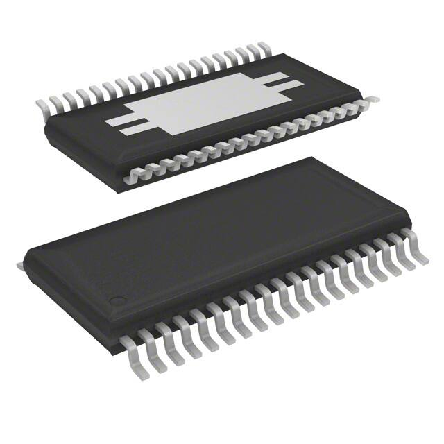


 工商网监
湘ICP备2023018690号
工商网监
湘ICP备2023018690号


