MILITARY DATA SHEET
Original Creation Date: 06/20/95
Last Update Date: 12/10/96
Last Major Revision Date: 06/20/95
MNLM709A-X REV 0B0
OPERATIONAL AMPLIFIER
General Description
The LM709 is a monolithic operational amplifier intended for general-purpose applications.
Operation is completely specified over the range of voltages commonly used for these
devices. The design, in addition to providing high gain, minimizes both offset voltage and
bias currents. Further, the class-B output stage gives a large output capability with
minimum power drain.
External components are used to frequency compensate the amplifier. Although the
unity-gain compensation network specified will make the amplifier unconditionally stable
in all feedback configurations, compensation can be tailored to optimize high-frequency
performance for any gain setting.
Industry Part Number
NS Part Numbers
LM709A
LM709AH/883
LM709AJ/883
LM709AW/883
Prime Die
LM709
Processing
Subgrp Description
MIL-STD-883, Method 5004
1
2
3
4
5
6
7
8A
8B
9
10
11
Quality Conformance Inspection
MIL-STD-883, Method 5005
1
Static tests at
Static tests at
Static tests at
Dynamic tests at
Dynamic tests at
Dynamic tests at
Functional tests at
Functional tests at
Functional tests at
Switching tests at
Switching tests at
Switching tests at
Temp ( oC)
+25
+125
-55
+25
+125
-55
+25
+125
-55
+25
+125
-55
�MILITARY DATA SHEET
MNLM709A-X REV 0B0
(Absolute Maximum Ratings)
(Note 1)
Supply Voltage
+18V
Power Dissipation
300mW
Differential Input Voltage
+5V
Input Voltage
+10V
Output Short-Circuit Duration (TA = +25 C)
5 Seconds
Storage Temperature Range
-65 C to +150 C
Lead Temperature (Soldering 10 Sec.)
300 C
Note 1:
Absolute Maximum Ratings indicate limits which if exceeded may result in damage.
Operating Ratings are conditions where the device is expected to be functional but
not necessarily within the guaranteed performance limits. For guaranteed
specifications and test conditions, see the Electrical Characteristics.
Recommended Operating Conditions
Junction Temperature Range
(Note 1)
-55 C to +150 C
Thermal Resistance
ThetaJA (H Package)
150 C/W
ThetaJC (H Package)
Note 1:
45 C/W
For operating at elevated temperatures, the device must be derated based on a 150 C
maximum junction temperature. For operating at elevated temperature, the device must
be derated based on thermal resistance ThetaJA, Tj(MAX) and TA.
2
�MILITARY DATA SHEET
MNLM709A-X REV 0B0
Electrical Characteristics
DC PARAMETERS
(The following conditions apply to all the following parameters, unless otherwise specified.)
DC: Vcc = +15V, Vcm = 0, Rs = 10K Ohms
SYMBOL
Vio
PARAMETER
Input Offset
Voltage
CONDITIONS
NOTES
PINNAME
MIN
Rs = 10K Ohms
Iib
UNIT
SUBGROUPS
2
mV
1
3
mV
2, 3
2
mV
1
3
mV
2, 3
Vcc = +9V
2
mV
1
Vcc = +9V
3
mV
2, 3
50
nA
1, 2
200
nA
3
Vcc = +9V
50
nA
1, 2
Vcc = +9V
200
nA
3
200
nA
1, 2
500
nA
3
Vcc = +9V
200
nA
1, 2
Vcc = +9V
500
nA
3
70
V/mV 1, 2,
3
100
uV/V 1, 2,
3
Rs = 0 Ohms
Iio
MAX
Input Offset
Current
Input Bias
Current
Avs
Large Voltage
Signal Gain
Rs=0 Ohms, RL=2K Ohms, -10V= +9V
CMRR
Common Mode
Rejection Ratio
-8V
很抱歉,暂时无法提供与“LM709AW/883”相匹配的价格&库存,您可以联系我们找货
免费人工找货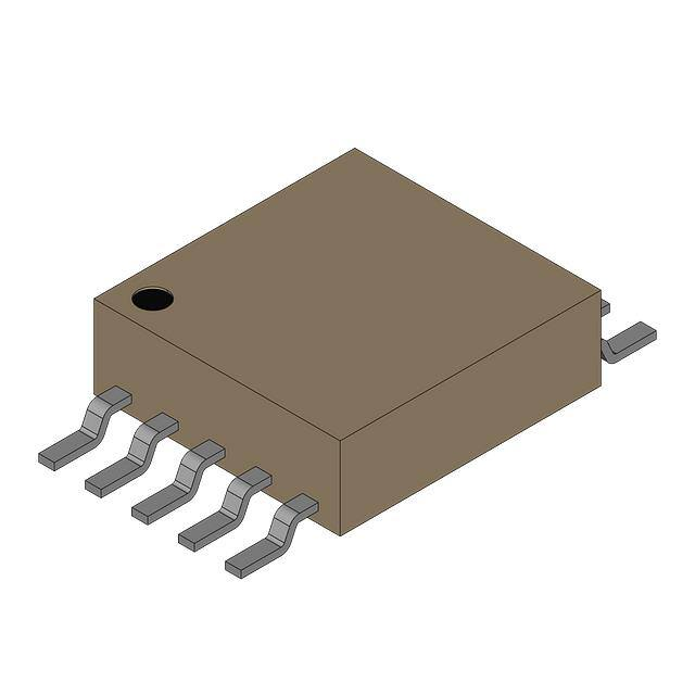


 工商网监
湘ICP备2023018690号
工商网监
湘ICP备2023018690号
