National Semiconductor is now part of
Texas Instruments.
Search http://www.ti.com/ for the latest technical
information and details on our current products and services.
�LMC6001
Ultra Ultra-Low Input Current Amplifier
General Description
Featuring 100% tested input currents of 25 fA max., low operating power, and ESD protection of 2000V, the LMC6001
achieves a new industry benchmark for low input current operational amplifiers. By tightly controlling the molding compound, National is able to offer this ultra-low input current in
a lower cost molded package.
To avoid long turn-on settling times common in other low input
current opamps, the LMC6001A is tested 3 times in the first
minute of operation. Even units that meet the 25 fA limit are
rejected if they drift.
Because of the ultra-low input current noise of 0.13 fA/√Hz,
the LMC6001 can provide almost noiseless amplification of
high resistance signal sources. Adding only 1 dB at 100 kΩ,
0.1 dB at 1 MΩ and 0.01 dB or less from 10 MΩ to 2,000
MΩ, the LMC6001 is an almost noiseless amplifier.
The LMC6001 is ideally suited for electrometer applications
requiring ultra-low input leakage such as sensitive photodetection transimpedance amplifiers and sensor amplifiers.
Since input referred noise is only 22 nV/√Hz, the LMC6001
can achieve higher signal to noise ratio than JFET input type
electrometer amplifiers. Other applications of the LMC6001
include long interval integrators, ultra-high input impedance
instrumentation amplifiers, and sensitive electrical-field measurement circuits.
Features
(Max limit, 25°C unless otherwise noted)
■ Input current (100% tested): 25 fA
■ Input current over temp.: 2 pA
■ Low power: 750 μA
■ Low VOS: 350 μV
■ Low noise: 22 nV/√Hz @1 kHz Typ.
Applications
■
■
■
■
Electrometer amplifier
Photodiode preamplifier
Ion detector
A.T.E. leakage testing
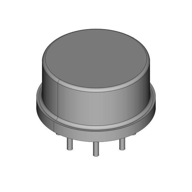
Connection Diagrams
8-Pin DIP
8-Pin Metal Can
1188701
Top View
1188702
Top View
Ordering Information
Package
Industrial Temperature Range
−40°C to +85°C
NSC Package
Drawing
8-Pin
Molded DIP
LMC6001AIN, LMC6001BIN,
LMC6001CIN
N08E
8-Pin
Metal Can
LMC6001AIH, LMC6001BIH
H08C
© 2009 National Semiconductor Corporation
11887
www.national.com
LMC6001 Ultra Ultra-Low Input Current Amplifier
November 4, 2009
�LMC6001
Absolute Maximum Ratings (Note 1)
Operating Ratings
If Military/Aerospace specified devices are required,
please contact the National Semiconductor Sales Office/
Distributors for availability and specifications.
Differential Input Voltage
Voltage at Input/Output Pin
Supply Voltage (V+ − V−)
Output Short Circuit to V+
Output Short Circuit to V−
Lead Temperature
(Soldering, 10 Sec.)
Storage Temperature
Junction Temperature
Current at Input Pin
Current at Output Pin
Current at Power Supply Pin
Power Dissipation
ESD Tolerance (Note 9)
(Note 1)
Temperature Range
LMC6001AI, LMC6001BI, LMC6001CI
−40°C ≤ TJ ≤ +85°C
Supply Voltage
±Supply Voltage
(V+) + 0.3V, (V−) − 0.3V
4.5V ≤ V+ ≤ 15.5V
Thermal Resistance (Note 11)
−0.3V to +16V
(Note 2, Note 10)
(Note 2)
260°C
−65°C to +150°C
150°C
±10 mA
±30 mA
40 mA
(Note 9)
2 kV
θJA, N Package
100°C/W
θJA, H Package
145°C/W
θJC, H Package
Power Dissipation
45°C/W
(Note 8)
DC Electrical Characteristics
Limits in standard typeface guaranteed for TJ = 25°C and limits in boldface type apply at the temperature extremes. Unless
otherwise specified, V+ = 5V, V− = 0V, VCM = 1.5V, and RL > 1M.
Symbol
IB
Conditions
Parameter
Input Current
Typical
(Note 4)
Either Input, VCM = 0V,
Input Offset Current
VOS
Input Offset Voltage
5
25
100
1000
4000
4000
1000
2000
2000
0.35
1.0
1.0
1.0
1.7
2.0
0.7
1.35
1.35
1.35
2.0
10
10
75
72
66
72
68
63
73
66
66
70
63
63
80
74
74
77
71
71
VS = ±5V, VCM = 0V
TCVOS
Input Offset
Units
2000
10
VS = ±5V
IOS
Limits (Note 5)
LMC6001AI LMC6001BI LMC6001CI
2.5
fA
mV
μV/°C
Voltage Drift
RIN
Input Resistance
CMRR
Common Mode
0V ≤ VCM ≤ 7.5V
Rejection Ratio
V+ = 10V
Positive Power Supply
5V ≤ V+ ≤ 15V
+PSRR
Tera Ω
>1
83
83
Rejection Ratio
−PSRR
Negative Power
0V ≥ V− ≥ −10V
94
Supply Rejection Ratio
AV
Large Signal
Sourcing, RL = 2 kΩ
400
300
300
Voltage Gain
(Note 6)
300
200
200
Sinking, RL = 2 kΩ
350
180
90
90
100
60
60
−0.4
−0.1
−0.1
−0.1
V
0
0
0
max
V+ − 1.9
V+ − 2.3
V+ − 2.3
V+ − 2.3
V
V+
V+
V+
1400
(Note 6)
VCM
dB
min
Input Common-Mode
V+ = 5V and 15V
Voltage
For CMRR ≥ 60 dB
www.national.com
2
− 2.5
− 2.5
− 2.5
V/mV
min
min
�VO
Conditions
Parameter
Output Swing
Typical
(Note 4)
V+ = 5V
4.75
4.75
V
4.67
4.67
min
0.10
0.14
0.17
0.20
0.24
0.20
0.24
V
max
14.63
14.50
14.37
14.37
V
14.34
14.25
14.25
min
0.26
0.35
0.45
0.44
0.56
0.44
0.56
V
max
22
16
13
13
10
8
8
16
13
13
13
10
10
28
23
23
RL = 2 kΩ to 7.5V
Output Current
Sourcing, V+ = 5V,
VO = 0V
Sinking,
V+
= 5V,
21
VO = 5V
Sourcing, V+ = 15V,
30
VO = 0V
IS
Supply Current
LMC6001AI LMC6001BI LMC6001CI
4.73
RL = 2 kΩ to 2.5V
IO
Units
4.80
4.87
V+ = 15V
Limits (Note 5)
22
18
18
Sinking, V+ = 15V,
VO = 13V (Note 10)
34
28
22
23
18
23
18
V+ = 5V, VO = 1.5V
450
750
750
750
900
900
900
850
850
850
950
950
950
V+ = 15V, VO = 7.5V
550
3
mA
min
μA
max
www.national.com
LMC6001
Symbol
�LMC6001
AC Electrical Characteristics
Limits in standard typeface guaranteed for TJ = 25°C and limits in boldface type apply at the temperature extremes. Unless
otherwise specified, V+ = 5V, V− = 0V, VCM = 1.5V and RL > 1M.
Symbol
SR
Parameter
Slew Rate
Limits (Note 5)
Typical
Conditions
(Note 7)
Units
(Note 4)
LM6001AI
LM6001BI
LM6001CI
1.5
0.8
0.8
0.8
0.6
0.6
0.6
V/μs
min
GBW
Gain-Bandwidth Product
1.3
MHz
φfm
Phase Margin
50
Deg
GM
Gain Margin
17
dB
en
Input-Referred Voltage Noise
F = 1 kHz
22
nV/√Hz
in
Input-Referred Current Noise
F = 1 kHz
0.13
fA/√Hz
THD
Total Harmonic Distortion
F = 10 kHz, AV = −10,
0.01
%
RL = 100 kΩ,
VO = 8 VPP
Note 1: Absolute Maximum Ratings indicate limits beyond which damage to the device may occur. Operating Ratings indicate conditions for which the device is
intended to be functional but do not guarantee specific performance limits. For guaranteed specifications and test conditions, see the Electrical Characteristics.
The guaranteed specifications apply only for the test conditions listed.
Note 2: Applies to both single supply and split supply operation. Continuous short circuit operation at elevated ambient temperature can result in exceeding the
maximum allowed junction temperature of 150°C. Output currents in excess of ±30 mA over long term may adversely affect reliability.
Note 3: The maximum power dissipation is a function of TJ(max), θJA, and TA. The maximum allowable power dissipation at any ambient temperature is
PD = (TJ(max) − TA)/θJA.
Note 4: Typical values represent the most likely parametric norm.
Note 5: All limits are guaranteed by testing or statistical analysis.
Note 6: V+ = 15V, VCM = 7.5V and RL connected to 7.5V. For Sourcing tests, 7.5V ≤ VO ≤ 11.5V. For Sinking tests, 2.5V ≤ VO ≤ 7.5V.
Note 7: V+ = 15V. Connected as Voltage Follower with 10V step input. Limit specified is the lower of the positive and negative slew rates.
Note 8: For operating at elevated temperatures the device must be derated based on the thermal resistance θJA with PD = (TJ − TA)/θJA.
Note 9: Human body model, 1.5 kΩ in series with 100 pF.
Note 10: Do not connect the output to V+, when V+ is greater than 13V or reliability will be adversely affected.
Note 11: All numbers apply for packages soldered directly into a printed circuit board.
www.national.com
4
�LMC6001
Typical Performance Characteristics
VS = ±7.5V, TA = 25°C, unless otherwise specified
Input Current vs. Temperature
Input Current vs. VCM VS = ±5V
1188716
1188717
Supply Current vs. Supply Voltage
Input Voltage vs.Output Voltage
1188718
1188719
Common Mode Rejection Ratio vs. Frequency
Power Supply Rejection Ratio vs. Frequency
1188721
1188720
5
www.national.com
�LMC6001
Input Voltage Noise vs. Frequency
Noise Figure vs. Source Resistance
1188722
1188723
Output Characteristics Sourcing Current
Output Characteristics Sinking Current
1188724
1188725
Gain and Phase Response vs. Temperature
(−55°C to +125°C)
Gain and Phase Response vs. Capacitive Load
with RL = 500 kΩ
1188726
www.national.com
1188727
6
�Inverting Small Signal Pulse Response
1188729
1188728
Inverting Large Signal Pulse Response
Non-Inverting Small Signal Pulse Response
1188730
1188731
Non-Inverting Large Signal Pulse Response
Stability vs. Capacitive Load
1188732
1188733
7
www.national.com
LMC6001
Open Loop Frequency Response
�LMC6001
dominant pole is affected by the resistive load on the amplifier.
Capacitive load driving capability can be optimized by using
an appropriate resistive load in parallel with the capacitive
load (see Typical Curves).
Direct capacitive loading will reduce the phase margin of
many op-amps. A pole in the feedback loop is created by the
combination of the op-amp's output impedance and the capacitive load. This pole induces phase lag at the unity-gain
crossover frequency of the amplifier resulting in either an oscillatory or underdamped pulse response. With a few external
components, op amps can easily indirectly drive capacitive
loads, as shown in Figure 2.
Applications Hints
AMPLIFIER TOPOLOGY
The LMC6001 incorporates a novel op-amp design topology
that enables it to maintain rail-to-rail output swing even when
driving a large load. Instead of relying on a push-pull unity
gain output buffer stage, the output stage is taken directly
from the internal integrator, which provides both low output
impedance and large gain. Special feed-forward compensation design techniques are incorporated to maintain stability
over a wider range of operating conditions than traditional opamps. These features make the LMC6001 both easier to
design with, and provide higher speed than products typically
found in this low power class.
COMPENSATING FOR INPUT CAPACITANCE
It is quite common to use large values of feedback resistance
for amplifiers with ultra-low input current, like the LMC6001.
Although the LMC6001 is highly stable over a wide range of
operating conditions, certain precautions must be met to
achieve the desired pulse response when a large feedback
resistor is used. Large feedback resistors with even small
values of input capacitance, due to transducers, photodiodes,
and circuit board parasitics, reduce phase margins.
When high input impedances are demanded, guarding of the
LMC6001 is suggested. Guarding input lines will not only reduce leakage, but lowers stray input capacitance as well.
(See Printed-Circuit-Board Layout for High Impedance
Work).
The effect of input capacitance can be compensated for by
adding a capacitor, Cf, around the feedback resistors (as in
Figure 1) such that:
1188706
FIGURE 2. LMC6001 Noninverting Gain of 10 Amplifier,
Compensated to Handle Capacitive Loads
In the circuit of Figure 2, R1 and C1 serve to counteract the
loss of phase margin by feeding the high frequency component of the output signal back to the amplifier's inverting input,
thereby preserving phase margin in the overall feedback loop.
Capacitive load driving capability is enhanced by using a
pullup resistor to V+ (Figure 3). Typically a pullup resistor conducting 500 μA or more will significantly improve capacitive
load responses. The value of the pullup resistor must be determined based on the current sinking capability of the amplifier with respect to the desired output swing. Open loop gain
of the amplifier can also be affected by the pullup resistor (see
Electrical Characteristics).
or
R1 CIN ≤ R2 Cf
Since it is often difficult to know the exact value of CIN, Cf can
be experimentally adjusted so that the desired pulse response is achieved. Refer to the LMC660 and LMC662 for a
more detailed discussion on compensating for input capacitance.
1188705
1188707
FIGURE 1. Cancelling the Effect of Input Capacitance
FIGURE 3. Compensating for Large Capacitive Loads
with a Pullup Resistor
CAPACITIVE LOAD TOLERANCE
All rail-to-rail output swing operational amplifiers have voltage
gain in the output stage. A compensation capacitor is normally
included in this integrator stage. The frequency location of the
www.national.com
8
�LMC6001
PRINTED-CIRCUIT-BOARD LAYOUT
FOR HIGH-IMPEDANCE WORK
It is generally recognized that any circuit which must operate
with less than 1000 pA of leakage current requires special
layout of the PC board. When one wishes to take advantage
of the ultra-low bias current of the LMC6001, typically less
than 10 fA, it is essential to have an excellent layout. Fortunately, the techniques of obtaining low leakages are quite
simple. First, the user must not ignore the surface leakage of
the PC board, even though it may sometimes appear acceptably low, because under conditions of high humidity or dust
or contamination, the surface leakage will be appreciable.
To minimize the effect of any surface leakage, lay out a ring
of foil completely surrounding the LMC6001's inputs and the
terminals of capacitors, diodes, conductors, resistors, relay
terminals, etc., connected to the op-amp's inputs, as in Figure
4. To have a significant effect, guard rings should be placed
on both the top and bottom of the PC board. This PC foil must
then be connected to a voltage which is at the same voltage
as the amplifier inputs, since no leakage current can flow between two points at the same potential. For example, a PC
board trace-to-pad resistance of 1012Ω, which is normally
considered a very large resistance, could leak 5 pA if the trace
were a 5V bus adjacent to the pad of the input.
This would cause a 500 times degradation from the
LMC6001's actual performance. If a guard ring is used and
held within 1 mV of the inputs, then the same resistance of
1012Ω will only cause 10 fA of leakage current. Even this small
amount of leakage will degrade the extremely low input current performance of the LMC6001. See Figure 5 for typical
connections of guard rings for standard op-amp configurations.
1188710
Non-Inverting Amplifier
1188711
Follower
FIGURE 5. Typical Connections of Guard Rings
The designer should be aware that when it is inappropriate to
lay out a PC board for the sake of just a few circuits, there is
another technique which is even better than a guard ring on
a PC board: Don't insert the amplifier's input pin into the board
at all, but bend it up in the air and use only air as an insulator.
Air is an excellent insulator. In this case you may have to
forego some of the advantages of PC board construction, but
the advantages are sometimes well worth the effort of using
point-to-point up-in-the-air wiring. See Figure 6.
1188712
(Input pins are lifted out of PC board and soldered directly to components.
All other pins connected to PC board).
1188708
FIGURE 6. Air Wiring
FIGURE 4. Examples of Guard
Ring in PC Board Layout
Another potential source of leakage that might be overlooked
is the device package. When the LMC6001 is manufactured,
the device is always handled with conductive finger cots. This
is to assure that salts and skin oils do not cause leakage paths
on the surface of the package. We recommend that these
same precautions be adhered to, during all phases of inspection, test and assembly.
LATCHUP
CMOS devices tend to be susceptible to latchup due to their
internal parasitic SCR effects. The (I/O) input and output pins
look similar to the gate of the SCR. There is a minimum current required to trigger the SCR gate lead. The LMC6001 is
designed to withstand 100 mA surge current on the I/O pins.
Some resistive method should be used to isolate any capacitance from supplying excess current to the I/O pins. In addition, like an SCR, there is a minimum holding current for any
1188709
Inverting Amplifier
9
www.national.com
�LMC6001
latchup mode. Limiting current to the supply pins will also inhibit latchup susceptibility.
micropower LMC6041 provides phase inversion and offset so
that the output is directly proportional to pH, over the full range
of the probe. The pH reading can now be directly displayed
on a low cost, low power digital panel meter. Total current
consumption will be about 1 mA for the whole system.
The micropower dual operational amplifier, LMC6042, would
optimize power consumption but not offer these advantages:
1. The LMC6001A guarantees a 25 fA limit on input current
at 25°C.
2. The input ESD protection diodes in the LMC6042 are
only rated at 500V while the LMC6001 has much more
robust protection that is rated at 2000V.
The setup and calibration is simple with no interactions to
cause problems.
1. Disconnect the pH probe and with R3 set to about midrange and the noninverting input of the LMC6001
grounded, adjust R8 until the output is 700 mV.
2. Apply −414.1 mV to the noninverting input of the
LMC6001. Adjust R3 for and output of 1400 mV. This
completes the calibration. As real pH probes may not
perform exactly to theory, minor gain and offset
adjustments should be made by trimming while
measuring a precision buffer solution.
Typical Applications
The extremely high input resistance, and low power consumption, of the LMC6001 make it ideal for applications that
require battery-powered instrumentation amplifiers. Examples of these types of applications are hand-held pH probes,
analytic medical instruments, electrostatic field detectors and
gas chromotographs.
TWO OPAMP, TEMPERATURE
COMPENSATED pH PROBE AMPLIFIER
The signal from a pH probe has a typical resistance between
10 MΩ and 1000 MΩ. Because of this high value, it is very
important that the amplifier input currents be as small as possible. The LMC6001 with less than 25 fA input current is an
ideal choice for this application.
The theoretical output of the standard Ag/AgCl pH probe is
59.16 mV/pH at 25°C with 0V out at a pH of 7.00. This output
is proportional to absolute temperature. To compensate for
this, a temperature compensating resistor, R1, is placed in the
feedback loop. This cancels the temperature dependence of
the probe. This resistor must be mounted where it will be at
the same temperature as the liquid being measured.
The LMC6001 amplifies the probe output providing a scaled
voltage of ±100 mV/pH from a pH of 7. The second opamp, a
1188715
R1 100k + 3500 ppm/°C (Note 12)
R2 68.1k
R3, 8 5k
R4, 9 100k
R5 36.5k
R6 619k
R7 97.6k
D1 LM4040D1Z-2.5
C1 2.2 μF
Note 12: (Micro-ohm style 137 or similar)
FIGURE 7. pH Probe Amplifier
20 fA and offset drift is less than 2.5 μV/°C. R2 provides a
simple means of adjusting gain over a wide range without degrading CMRR. R7 is an initial trim used to maximize CMRR
without using super precision matched resistors. For good
CMRR over temperature, low drift resistors should be used.
ULTRA-LOW INPUT CURRENT INSTRUMENTATION
AMPLIFIER
Figure 8 shows an instrumentation amplifier that features high
differential and common mode input resistance (>1014Ω),
0.01% gain accuracy at AV = 1000, excellent CMRR with 1
MΩ imbalance in source resistance. Input current is less than
www.national.com
10
�LMC6001
1188713
If R1 = R5, R3 = R6, and R4 = R7; then
∴AV ≈ 100 for circuit shown (R2 = 9.85k).
FIGURE 8. Instrumentation Amplifier
11
www.national.com
�LMC6001
Physical Dimensions inches (millimeters) unless otherwise noted
8-Pin Metal Can Package (H)
NS Package Number H08C
8-Pin Molded Dual-In-Line Package
NS Package Number N08E
www.national.com
12
�LMC6001
Notes
13
www.national.com
�LMC6001 Ultra Ultra-Low Input Current Amplifier
Notes
For more National Semiconductor product information and proven design tools, visit the following Web sites at:
Products
Design Support
Amplifiers
www.national.com/amplifiers
WEBENCH® Tools
www.national.com/webench
Audio
www.national.com/audio
App Notes
www.national.com/appnotes
Clock and Timing
www.national.com/timing
Reference Designs
www.national.com/refdesigns
Data Converters
www.national.com/adc
Samples
www.national.com/samples
Interface
www.national.com/interface
Eval Boards
www.national.com/evalboards
LVDS
www.national.com/lvds
Packaging
www.national.com/packaging
Power Management
www.national.com/power
Green Compliance
www.national.com/quality/green
Switching Regulators
www.national.com/switchers
Distributors
www.national.com/contacts
LDOs
www.national.com/ldo
Quality and Reliability
www.national.com/quality
LED Lighting
www.national.com/led
Feedback/Support
www.national.com/feedback
Voltage Reference
www.national.com/vref
Design Made Easy
www.national.com/easy
www.national.com/powerwise
Solutions
www.national.com/solutions
Mil/Aero
www.national.com/milaero
PowerWise® Solutions
Serial Digital Interface (SDI) www.national.com/sdi
Temperature Sensors
www.national.com/tempsensors SolarMagic™
www.national.com/solarmagic
Wireless (PLL/VCO)
www.national.com/wireless
www.national.com/training
PowerWise® Design
University
THE CONTENTS OF THIS DOCUMENT ARE PROVIDED IN CONNECTION WITH NATIONAL SEMICONDUCTOR CORPORATION
(“NATIONAL”) PRODUCTS. NATIONAL MAKES NO REPRESENTATIONS OR WARRANTIES WITH RESPECT TO THE ACCURACY
OR COMPLETENESS OF THE CONTENTS OF THIS PUBLICATION AND RESERVES THE RIGHT TO MAKE CHANGES TO
SPECIFICATIONS AND PRODUCT DESCRIPTIONS AT ANY TIME WITHOUT NOTICE. NO LICENSE, WHETHER EXPRESS,
IMPLIED, ARISING BY ESTOPPEL OR OTHERWISE, TO ANY INTELLECTUAL PROPERTY RIGHTS IS GRANTED BY THIS
DOCUMENT.
TESTING AND OTHER QUALITY CONTROLS ARE USED TO THE EXTENT NATIONAL DEEMS NECESSARY TO SUPPORT
NATIONAL’S PRODUCT WARRANTY. EXCEPT WHERE MANDATED BY GOVERNMENT REQUIREMENTS, TESTING OF ALL
PARAMETERS OF EACH PRODUCT IS NOT NECESSARILY PERFORMED. NATIONAL ASSUMES NO LIABILITY FOR
APPLICATIONS ASSISTANCE OR BUYER PRODUCT DESIGN. BUYERS ARE RESPONSIBLE FOR THEIR PRODUCTS AND
APPLICATIONS USING NATIONAL COMPONENTS. PRIOR TO USING OR DISTRIBUTING ANY PRODUCTS THAT INCLUDE
NATIONAL COMPONENTS, BUYERS SHOULD PROVIDE ADEQUATE DESIGN, TESTING AND OPERATING SAFEGUARDS.
EXCEPT AS PROVIDED IN NATIONAL’S TERMS AND CONDITIONS OF SALE FOR SUCH PRODUCTS, NATIONAL ASSUMES NO
LIABILITY WHATSOEVER, AND NATIONAL DISCLAIMS ANY EXPRESS OR IMPLIED WARRANTY RELATING TO THE SALE
AND/OR USE OF NATIONAL PRODUCTS INCLUDING LIABILITY OR WARRANTIES RELATING TO FITNESS FOR A PARTICULAR
PURPOSE, MERCHANTABILITY, OR INFRINGEMENT OF ANY PATENT, COPYRIGHT OR OTHER INTELLECTUAL PROPERTY
RIGHT.
LIFE SUPPORT POLICY
NATIONAL’S PRODUCTS ARE NOT AUTHORIZED FOR USE AS CRITICAL COMPONENTS IN LIFE SUPPORT DEVICES OR
SYSTEMS WITHOUT THE EXPRESS PRIOR WRITTEN APPROVAL OF THE CHIEF EXECUTIVE OFFICER AND GENERAL
COUNSEL OF NATIONAL SEMICONDUCTOR CORPORATION. As used herein:
Life support devices or systems are devices which (a) are intended for surgical implant into the body, or (b) support or sustain life and
whose failure to perform when properly used in accordance with instructions for use provided in the labeling can be reasonably expected
to result in a significant injury to the user. A critical component is any component in a life support device or system whose failure to perform
can be reasonably expected to cause the failure of the life support device or system or to affect its safety or effectiveness.
National Semiconductor and the National Semiconductor logo are registered trademarks of National Semiconductor Corporation. All other
brand or product names may be trademarks or registered trademarks of their respective holders.
Copyright© 2009 National Semiconductor Corporation
For the most current product information visit us at www.national.com
National Semiconductor
Americas Technical
Support Center
Email: support@nsc.com
Tel: 1-800-272-9959
www.national.com
National Semiconductor Europe
Technical Support Center
Email: europe.support@nsc.com
National Semiconductor Asia
Pacific Technical Support Center
Email: ap.support@nsc.com
National Semiconductor Japan
Technical Support Center
Email: jpn.feedback@nsc.com
�


 工商网监
湘ICP备2023018690号
工商网监
湘ICP备2023018690号
