LMC6034
www.ti.com
SNOS608C – MAY 1998 – REVISED MARCH 2013
LMC6034 CMOS Quad Operational Amplifier
Check for Samples: LMC6034
FEATURES
DESCRIPTION
•
•
•
•
•
•
•
•
•
•
The LMC6034 is a CMOS quad operational amplifier
which can operate from either a single supply or dual
supplies. Its performance features include an input
common-mode range that reaches ground, low input
bias current, and high voltage gain into realistic loads,
such as 2 kΩ and 600Ω.
1
2
Specified for 2 kΩ and 600Ω Loads
High Voltage Gain: 126 dB
Low Offset Voltage Drift: 2.3 μV/°C
Ultra Low Input Bias Current: 40 fA
Input Common-Mode Range Includes V−
Operating Range from +5V to +15V Supply
ISS = 400 μA/Amplifier; Independent of V+
Low Distortion: 0.01% at 10 kHz
Slew Rate: 1.1 V/μs
Improved Performance Over TLC274
This chip is built with National's advanced DoublePoly Silicon-Gate CMOS process.
See the LMC6032 datasheet for a CMOS dual
operational amplifier with these same features. For
higher performance characteristics refer to the
LMC660.
APPLICATIONS
•
•
•
•
•
High-Impedance Buffer or Preamplifier
Current-to-Voltage Converter
Long-Term Integrator
Sample-and-Hold Circuit
Medical Instrumentation
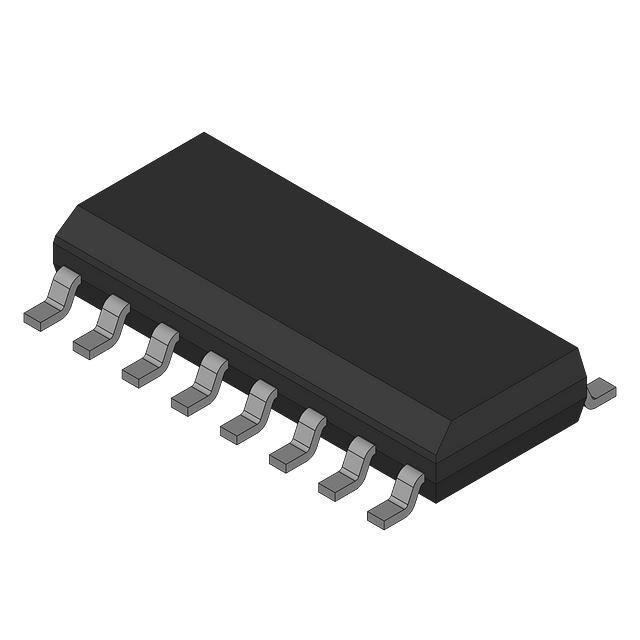
Connection Diagram
Figure 1. 14-Pin SOIC (Top View)
Guard Ring Connections – Non-Inverting Amplifier
1
2
Please be aware that an important notice concerning availability, standard warranty, and use in critical applications of
Texas Instruments semiconductor products and disclaimers thereto appears at the end of this data sheet.
All trademarks are the property of their respective owners.
PRODUCTION DATA information is current as of publication date.
Products conform to specifications per the terms of the Texas
Instruments standard warranty. Production processing does not
necessarily include testing of all parameters.
Copyright © 1998–2013, Texas Instruments Incorporated
�LMC6034
SNOS608C – MAY 1998 – REVISED MARCH 2013
www.ti.com
These devices have limited built-in ESD protection. The leads should be shorted together or the device placed in conductive foam
during storage or handling to prevent electrostatic damage to the MOS gates.
ABSOLUTE MAXIMUM RATINGS (1) (2)
Differential Input Voltage
±Supply Voltage
Supply Voltage (V+ − V−)
16V
Output Short Circuit to V+
See (3)
Output Short Circuit to V−
See (4)
Lead Temperature (Soldering, 10 sec.)
260°C
−65°C to +150°C
Storage Temperature Range
See (5)
Power Dissipation
−
+
(V ) +0.3V, (V ) −0.3V
Voltage at Output/Input Pin
Current at Output Pin
±18 mA
Current at Input Pin
±5 mA
Current at Power Supply Pin
35 mA
Junction Temperature (5)
150°C
ESD Tolerance (6)
1000V
(1)
Absolute Maximum Ratings indicate limits beyond which damage to the component may occur. Operating Ratings indicate conditions for
which the device is intended to be functional, but do not guarantee specific performance limits. For guaranteed specifications and test
conditions, see the Electrical Characteristics. The guaranteed specifications apply only for the test conditions listed.
If Military/Aerospace specified devices are required, please contact the TI Sales Office/ Distributors for availability and specifications.
Do not connect output to V+, when V+ is greater than 13V or reliability may be adversely affected.
Applies to both single-supply and split-supply operation. Continuous short circuit operation at elevated ambient temperature and/or
multiple Op Amp shorts can result in exceeding the maximum allowed junction temperature of 150°C. Output currents in excess of ±30
mA over long term may adversely affect reliability.
The maximum power dissipation is a function of TJ(max), θJA, TA. The maximum allowable power dissipation at any ambient temperature
is PD = (TJ(max)–TA)/θJA.
Human body model, 100 pF discharged through a 1.5 kΩ resistor.
(2)
(3)
(4)
(5)
(6)
OPERATING RATINGS (1)
−40°C ≤ TJ ≤ +85°C
Temperature Range
Supply Voltage Range
4.75V to 15.5V
See (2)
Power Dissipation
Thermal Resistance (θJA)
(1)
(3)
14-Pin SOIC
115°C/W
Absolute Maximum Ratings indicate limits beyond which damage to the component may occur. Operating Ratings indicate conditions for
which the device is intended to be functional, but do not guarantee specific performance limits. For guaranteed specifications and test
conditions, see the Electrical Characteristics. The guaranteed specifications apply only for the test conditions listed.
For operating at elevated temperatures the device must be derated based on the thermal resistance θJA with PD = (TJ − TA)/θJA.
All numbers apply for packages soldered directly into a PC board.
(2)
(3)
DC ELECTRICAL CHARACTERISTICS
Unless otherwise specified, all limits guaranteed for TJ = 25°C. Boldface limits apply at the temperature extremes. V+ = 5V,
V− = GND = 0V, VCM = 1.5V, VOUT = 2.5V, and RL > 1M unless otherwise specified.
Symbol
Parameter
Conditions
Typical (1)
LMC6034I
Units
Limit (2)
VOS
Input Offset Voltage
1
9
ΔVOS/ΔT
Input Offset Voltage
2.3
μV/°C
0.04
pA
11
mV
max
Average Drift
IB
Input Bias Current
200
(1)
(2)
2
max
Typical values represent the most likely parametric norm.
All limits are guaranteed at room temperature (standard type face) or at operating temperature extremes (bold type face).
Submit Documentation Feedback
Copyright © 1998–2013, Texas Instruments Incorporated
Product Folder Links: LMC6034
�LMC6034
www.ti.com
SNOS608C – MAY 1998 – REVISED MARCH 2013
DC ELECTRICAL CHARACTERISTICS (continued)
Unless otherwise specified, all limits guaranteed for TJ = 25°C. Boldface limits apply at the temperature extremes. V+ = 5V,
V− = GND = 0V, VCM = 1.5V, VOUT = 2.5V, and RL > 1M unless otherwise specified.
Symbol
Parameter
Conditions
Typical (1)
LMC6034I
Units
Limit (2)
IOS
Input Offset Current
0.01
pA
100
RIN
Input Resistance
CMRR
Common Mode
+PSRR
−PSRR
>1
0V ≤ VCM ≤ 12V
TeraΩ
83
+
Rejection Ratio
V = 15V
Positive Power Supply
5V ≤ V+ ≤ 15V
Rejection Ratio
VO = 2.5V
Negative Power Supply
0V ≤ V− ≤ −10V
83
94
AV
Input Common-Mode
V+ = 5V & 15V
Voltage Range
For CMRR ≥ 50 dB
Large Signal Voltage Gain
RL = 2 kΩ (3)
RL = 600Ω
Output Voltage Swing
dB
60
min
−0.4
−0.1
V
0
max
V+ − 1.9
V+ − 2.3
V
V+ − 2.6
min
200
V/mV
2000
1000
100
min
90
V/mV
40
min
100
V/mV
75
min
Sinking
250
50
V/mV
20
min
V+ = 5V
4.87
4.20
V
4.00
min
0.25
V
0.35
max
RL = 2 kΩ to 2.5V
0.10
V+ = 5V
4.61
RL = 600Ω to 2.5V
0.30
V+ = 15V
14.63
RL = 2 kΩ to 7.5V
0.26
V+ = 15V
13.90
RL = 600Ω to 7.5V
0.79
(3)
min
63
dB
Sourcing
VO
60
min
500
(3)
dB
70
Sourcing
Sinking
63
74
Rejection Ratio
VCM
max
4.00
V
3.80
min
0.63
V
0.75
max
13.50
V
13.00
min
0.45
V
0.55
max
12.50
V
12.00
min
1.45
V
1.75
max
V+ = 15V, VCM = 7.5V, and RL connected to 7.5V. For Sourcing tests, 7.5V ≤ VO ≤ 11.5V. For Sinking tests, 2.5V ≤ VO ≤ 7.5V.
Submit Documentation Feedback
Copyright © 1998–2013, Texas Instruments Incorporated
Product Folder Links: LMC6034
3
�LMC6034
SNOS608C – MAY 1998 – REVISED MARCH 2013
www.ti.com
DC ELECTRICAL CHARACTERISTICS (continued)
Unless otherwise specified, all limits guaranteed for TJ = 25°C. Boldface limits apply at the temperature extremes. V+ = 5V,
V− = GND = 0V, VCM = 1.5V, VOUT = 2.5V, and RL > 1M unless otherwise specified.
Symbol
Parameter
Conditions
Typical (1)
LMC6034I
Units
Limit (2)
IO
V+ = 5V
Output Current
22
Sourcing, VO = 0V
Sinking, VO = 5V
V+ = 15V
21
40
Sourcing, VO = 0V
IS
Supply Current
mA
9
min
13
mA
9
min
23
mA
15
min
Sinking, VO = 13V (4)
39
23
mA
15
min
All Four Amplifiers
1.5
2.7
mA
3.0
max
VO = 1.5V
(4)
13
Do not connect output to V+, when V+ is greater than 13V or reliability may be adversely affected.
AC ELECTRICAL CHARACTERISTICS
Unless otherwise specified, all limits guaranteed for TJ = 25°C. Boldface limits apply at the temperature extremes. V+ = 5V,
V− = GND = 0V, VCM = 1.5V, VOUT = 2.5V, and RL > 1M unless otherwise specified.
Symbol
Parameter
Conditions
Typical (1)
LMC6034I
Units
Limit (2)
See (3)
SR
Slew Rate
1.1
0.8
GBW
Gain-Bandwidth Product
1.4
MHz
φM
Phase Margin
50
Deg
GM
Gain Margin
17
dB
0.4
V/μs
min
Amp-to-Amp Isolation
See (4)
130
dB
en
Input-Referred Voltage Noise
F = 1 kHz
22
nV/√Hz
in
Input-Referred Current Noise
F = 1 kHz
0.0002
pA/√Hz
THD
Total Harmonic Distortion
F = 10 kHz, AV = −10
0.01
%
RL = 2 kΩ, VO = 8 VPP
±5V Supply
(1)
(2)
(3)
(4)
4
Typical values represent the most likely parametric norm.
All limits are guaranteed at room temperature (standard type face) or at operating temperature extremes (bold type face).
V+ = 15V. Connected as Voltage Follower with 10V step input. Number specified is the slower of the positive and negative slew rates.
Input referred. V+ = 15V and RL = 10 kΩ connected to V+/2. Each amp excited in turn with 1 kHz to produce VO = 13 VPP.
Submit Documentation Feedback
Copyright © 1998–2013, Texas Instruments Incorporated
Product Folder Links: LMC6034
�LMC6034
www.ti.com
SNOS608C – MAY 1998 – REVISED MARCH 2013
TYPICAL PERFORMANCE CHARACTERISTICS
VS = ±7.5V, TA = 25°C unless otherwise specified
Note: Avoid resistive loads of less than 500Ω, as they may cause instability
Supply Current
vs Supply Voltage
Input Bias Current
Figure 2.
Figure 3.
Output Characteristics
Current Sinking
Output Characteristics
Current Sourcing
Figure 4.
Figure 5.
Input Voltage Noise
vs Frequency
CMRR
vs
Frequency
Figure 6.
Figure 7.
Submit Documentation Feedback
Copyright © 1998–2013, Texas Instruments Incorporated
Product Folder Links: LMC6034
5
�LMC6034
SNOS608C – MAY 1998 – REVISED MARCH 2013
www.ti.com
TYPICAL PERFORMANCE CHARACTERISTICS (continued)
VS = ±7.5V, TA = 25°C unless otherwise specified
Note: Avoid resistive loads of less than 500Ω, as they may cause instability
Open-Loop Frequency
Response
Frequency Response
vs Capacitive Load
Figure 8.
Figure 9.
Non-Inverting Large Signal
Pulse Response
Stability vs
Capacitive Load
Figure 10.
Figure 11.
Stability vs
Capacitive Load
Figure 12.
6
Submit Documentation Feedback
Copyright © 1998–2013, Texas Instruments Incorporated
Product Folder Links: LMC6034
�LMC6034
www.ti.com
SNOS608C – MAY 1998 – REVISED MARCH 2013
APPLICATIONS HINT
Amplifier Topology
The topology chosen for the LMC6034, shown in Figure 13, is unconventional (compared to general-purpose op
amps) in that the traditional unity-gain buffer output stage is not used; instead, the output is taken directly from
the output of the integrator, to allow a larger output swing. Since the buffer traditionally delivers the power to the
load, while maintaining high op amp gain and stability, and must withstand shorts to either rail, these tasks now
fall to the integrator.
As a result of these demands, the integrator is a compound affair with an embedded gain stage that is doubly fed
forward (via Cf and Cff) by a dedicated unity-gain compensation driver. In addition, the output portion of the
integrator is a push-pull configuration for delivering heavy loads. While sinking current the whole amplifier path
consists of three gain stages with one stage fed forward, whereas while sourcing the path contains four gain
stages with two fed forward.
Figure 13. LMC6034 Circuit Topology (Each Amplifier)
The large signal voltage gain while sourcing is comparable to traditional bipolar op amps, even with a 600Ω load.
The gain while sinking is higher than most CMOS op amps, due to the additional gain stage; however, under
heavy load (600Ω) the gain will be reduced as indicated in the Electrical Characteristics.
Compensating Input Capacitance
The high input resistance of the LMC6034 op amps allows the use of large feedback and source resistor values
without losing gain accuracy due to loading. However, the circuit will be especially sensitive to its layout when
these large-value resistors are used.
Every amplifier has some capacitance between each input and AC ground, and also some differential
capacitance between the inputs. When the feedback network around an amplifier is resistive, this input
capacitance (along with any additional capacitance due to circuit board traces, the socket, etc.) and the feedback
resistors create a pole in the feedback path. In the following General Operational Amplifier circuit, the frequency
of this pole is
(1)
where CS is the total capacitance at the inverting input, including amplifier input capcitance and any stray
capacitance from the IC socket (if one is used), circuit board traces, etc., and RP is the parallel combination of RF
and RIN. This formula, as well as all formulae derived below, apply to inverting and non-inverting op-amp
configurations.
When the feedback resistors are smaller than a few kΩ, the frequency of the feedback pole will be quite high,
since CS is generally less than 10 pF. If the frequency of the feedback pole is much higher than the “ideal”
closed-loop bandwidth (the nominal closed-loop bandwidth in the absence of CS), the pole will have a negligible
effect on stability, as it will add only a small amount of phase shift.
However, if the feedback pole is less than approximately 6 to 10 times the “ideal” −3 dB frequency, a feedback
capacitor, CF, should be connected between the output and the inverting input of the op amp. This condition can
also be stated in terms of the amplifier's low-frequency noise gain: To maintain stability a feedback capacitor will
probably be needed if
Submit Documentation Feedback
Copyright © 1998–2013, Texas Instruments Incorporated
Product Folder Links: LMC6034
7
�LMC6034
SNOS608C – MAY 1998 – REVISED MARCH 2013
www.ti.com
(2)
where
(3)
is the amplifier's low-frequency noise gain and GBW is the amplifier's gain bandwidth product. An amplifier's lowfrequency noise gain is represented by the formula
(4)
regardless of whether the amplifier is being used in inverting or non-inverting mode. Note that a feedback
capacitor is more likely to be needed when the noise gain is low and/or the feedback resistor is large.
If the above condition is met (indicating a feedback capacitor will probably be needed), and the noise gain is
large enough that:
(5)
the following value of feedback capacitor is recommended:
(6)
If
(7)
the feedback capacitor should be:
(8)
Note that these capacitor values are usually significantly smaller than those given by the older, more
conservative formula:
(9)
CS consists of the amplifier's input capacitance plus any stray capacitance from the circuit board and socket. CF
compensates for the pole caused by CS and the feedback resistors.
Figure 14. General Operational Amplifier Circuit
8
Submit Documentation Feedback
Copyright © 1998–2013, Texas Instruments Incorporated
Product Folder Links: LMC6034
�LMC6034
www.ti.com
SNOS608C – MAY 1998 – REVISED MARCH 2013
Using the smaller capacitors will give much higher bandwidth with little degradation of transient response. It may
be necessary in any of the above cases to use a somewhat larger feedback capacitor to allow for unexpected
stray capacitance, or to tolerate additional phase shifts in the loop, or excessive capacitive load, or to decrease
the noise or bandwidth, or simply because the particular circuit implementation needs more feedback
capacitance to be sufficiently stable. For example, a printed circuit board's stray capacitance may be larger or
smaller than the breadboard's, so the actual optimum value for CF may be different from the one estimated using
the breadboard. In most cases, the values of CF should be checked on the actual circuit, starting with the
computed value.
Capacitive Load Tolerance
Like many other op amps, the LMC6034 may oscillate when its applied load appears capacitive. The threshold of
oscillation varies both with load and circuit gain. The configuration most sensitive to oscillation is a unity-gain
follower. See Typical Performance Characteristics.
The load capacitance interacts with the op amp's output resistance to create an additional pole. If this pole
frequency is sufficiently low, it will degrade the op amp's phase margin so that the amplifier is no longer stable at
low gains. As shown in Figure 15, the addition of a small resistor (50Ω to 100Ω) in series with the op amp's
output, and a capacitor (5 pF to 10 pF) from inverting input to output pins, returns the phase margin to a safe
value without interfering with lower-frequency circuit operation. Thus larger values of capacitance can be
tolerated without oscillation. Note that in all cases, the output will ring heavily when the load capacitance is near
the threshold for oscillation.
Figure 15. Rx, Cx Improve Capacitive Load Tolerance
Capacitive load driving capability is enhanced by using a pull up resistor to V+ (Figure 16). Typically a pull up
resistor conducting 500 μA or more will significantly improve capacitive load responses. The value of the pull up
resistor must be determined based on the current sinking capability of the amplifier with respect to the desired
output swing. Open loop gain of the amplifier can also be affected by the pull up resistor (see Electrical
Characteristics).
Figure 16. Compensating for Large Capacitive Loads with a Pull Up Resistor
PRINTED-CIRCUIT-BOARD LAYOUT FOR HIGH-IMPEDANCE WORK
It is generally recognized that any circuit which must operate with less than 1000 pA of leakage current requires
special layout of the PC board. When one wishes to take advantage of the ultra-low bias current of the
LMC6034, typically less than 0.04 pA, it is essential to have an excellent layout. Fortunately, the techniques for
obtaining low leakages are quite simple. First, the user must not ignore the surface leakage of the PC board,
even though it may sometimes appear acceptably low, because under conditions of high humidity or dust or
contamination, the surface leakage will be appreciable.
Submit Documentation Feedback
Copyright © 1998–2013, Texas Instruments Incorporated
Product Folder Links: LMC6034
9
�LMC6034
SNOS608C – MAY 1998 – REVISED MARCH 2013
www.ti.com
To minimize the effect of any surface leakage, lay out a ring of foil completely surrounding the LMC6034's inputs
and the terminals of capacitors, diodes, conductors, resistors, relay terminals, etc. connected to the op-amp's
inputs. See Figure 17 . To have a significant effect, guard rings should be placed on both the top and bottom of
the PC board. This PC foil must then be connected to a voltage which is at the same voltage as the amplifier
inputs, since no leakage current can flow between two points at the same potential. For example, a PC board
trace-to-pad resistance of 1012Ω, which is normally considered a very large resistance, could leak 5 pA if the
trace were a 5V bus adjacent to the pad of an input. This would cause a 100 times degradation from the
LMC6034's actual performance. However, if a guard ring is held within 5 mV of the inputs, then even a
resistance of 1011Ω would cause only 0.05 pA of leakage current, or perhaps a minor (2:1) degradation of the
amplifier's performance. See Figure 18, Figure 19 and , Figure 20 for typical connections of guard rings for
standard op-amp configurations. If both inputs are active and at high impedance, the guard can be tied to ground
and still provide some protection; see Figure 21.
Figure 17. Example of Guard Ring in P.C. Board Layout
Figure 18. Guard Ring Connections Inverting Amplifier
Figure 19. Guard Ring Connections Non-Inverting Amplifier
Figure 20. Guard Ring Connections Follower
10
Submit Documentation Feedback
Copyright © 1998–2013, Texas Instruments Incorporated
Product Folder Links: LMC6034
�LMC6034
www.ti.com
SNOS608C – MAY 1998 – REVISED MARCH 2013
Figure 21. Guard Ring Connections Howland Current Pump
The designer should be aware that when it is inappropriate to lay out a PC board for the sake of just a few
circuits, there is another technique which is even better than a guard ring on a PC board: Don't insert the
amplifier's input pin into the board at all, but bend it up in the air and use only air as an insulator. Air is an
excellent insulator. In this case you may have to forego some of the advantages of PC board construction, but
the advantages are sometimes well worth the effort of using point-to-point up-in-the-air wiring. See Figure 22.
(Input pins are lifted out of PC board and soldered directly to components. All other pins connected to PC board.)
Figure 22. Air Wiring
BIAS CURRENT TESTING
The test method of Figure 23 is appropriate for bench-testing bias current with reasonable accuracy. To
understand its operation, first close switch S2 momentarily. When S2 is opened, then
(10)
Figure 23. Simple Input Bias Current Test Circuit
A suitable capacitor for C2 would be a 5 pF or 10 pF silver mica, NPO ceramic, or air-dielectric. When
determining the magnitude of Ib−, the leakage of the capacitor and socket must be taken into account. Switch S2
should be left shorted most of the time, or else the dielectric absorption of the capacitor C2 could cause errors.
Submit Documentation Feedback
Copyright © 1998–2013, Texas Instruments Incorporated
Product Folder Links: LMC6034
11
�LMC6034
SNOS608C – MAY 1998 – REVISED MARCH 2013
www.ti.com
Similarly, if S1 is shorted momentarily (while leaving S2 shorted)
(11)
where Cx is the stray capacitance at the + input.
Typical Single-Supply Applications
(V+ = 5.0 VDC)
Additional single-supply applications ideas can be found in the LM324 datasheet. The LMC6034 is pin-for-pin
compatible with the LM324 and offers greater bandwidth and input resistance over the LM324. These features
will improve the performance of many existing single-supply applications. Note, however, that the supply voltage
range of the LMC6034 is smaller than that of the LM324.
Figure 24. Low-Leakage Sample-and-Hold
Figure 25. Instrumentation Amplifier
(12)
(13)
For good CMRR over temperature, low drift resistors should be used. Matching of R3 to R6 and R4 to R7 affect
CMRR. Gain may be adjusted through R2. CMRR may be adjusted through R7.
12
Submit Documentation Feedback
Copyright © 1998–2013, Texas Instruments Incorporated
Product Folder Links: LMC6034
�LMC6034
www.ti.com
SNOS608C – MAY 1998 – REVISED MARCH 2013
(V+ = 5.0 VDC)
Figure 26. Sine-Wave Oscillator
Oscillator frequency is determined by R1, R2, C1, and C2:
fosc = 1/2πRC, where R = R1 = R2 and C = C1 = C2.
This circuit, as shown, oscillates at 2.0 kHz with a peak-to-peak output swing of 4.0V.
Figure 27. 1 Hz Square-Wave Oscillator
Figure 28. Power Amplifier
Submit Documentation Feedback
Copyright © 1998–2013, Texas Instruments Incorporated
Product Folder Links: LMC6034
13
�LMC6034
SNOS608C – MAY 1998 – REVISED MARCH 2013
www.ti.com
(V+ = 5.0 VDC)
fO = 10 Hz
Q = 2.1
Gain = −8.8
Figure 29. 10 Hz Bandpass Filter
fc = 10 Hz
d = 0.895
Gain = 1
2 dB passband ripple
Figure 30. 10 Hz High-Pass Filter
fc = 1 Hz
d = 1.414
Gain = 1.57
Figure 31. 1 Hz Low-Pass Filter (Maximally Flat, Dual Supply Only)
14
Submit Documentation Feedback
Copyright © 1998–2013, Texas Instruments Incorporated
Product Folder Links: LMC6034
�LMC6034
www.ti.com
SNOS608C – MAY 1998 – REVISED MARCH 2013
(V+ = 5.0 VDC)
Gain = −46.8
Output offset voltage reduced to the level of the input offset voltage of the bottom amplifier(typically 1 mV).
Figure 32. High Gain Amplifier with Offset Voltage Reduction
Submit Documentation Feedback
Copyright © 1998–2013, Texas Instruments Incorporated
Product Folder Links: LMC6034
15
�LMC6034
SNOS608C – MAY 1998 – REVISED MARCH 2013
www.ti.com
REVISION HISTORY
Changes from Revision B (March 2013) to Revision C
•
16
Page
Changed layout of National Data Sheet to TI format .......................................................................................................... 15
Submit Documentation Feedback
Copyright © 1998–2013, Texas Instruments Incorporated
Product Folder Links: LMC6034
�PACKAGE OPTION ADDENDUM
www.ti.com
6-Aug-2021
PACKAGING INFORMATION
Orderable Device
Status
(1)
Package Type Package Pins Package
Drawing
Qty
Eco Plan
(2)
Lead finish/
Ball material
MSL Peak Temp
Op Temp (°C)
Device Marking
(3)
(4/5)
(6)
LMC6034IM/NOPB
ACTIVE
SOIC
D
14
55
RoHS & Green
SN
Level-1-260C-UNLIM
-40 to 85
LMC6034IM
LMC6034IMX/NOPB
ACTIVE
SOIC
D
14
2500
RoHS & Green
SN
Level-1-260C-UNLIM
-40 to 85
LMC6034IM
(1)
The marketing status values are defined as follows:
ACTIVE: Product device recommended for new designs.
LIFEBUY: TI has announced that the device will be discontinued, and a lifetime-buy period is in effect.
NRND: Not recommended for new designs. Device is in production to support existing customers, but TI does not recommend using this part in a new design.
PREVIEW: Device has been announced but is not in production. Samples may or may not be available.
OBSOLETE: TI has discontinued the production of the device.
(2)
RoHS: TI defines "RoHS" to mean semiconductor products that are compliant with the current EU RoHS requirements for all 10 RoHS substances, including the requirement that RoHS substance
do not exceed 0.1% by weight in homogeneous materials. Where designed to be soldered at high temperatures, "RoHS" products are suitable for use in specified lead-free processes. TI may
reference these types of products as "Pb-Free".
RoHS Exempt: TI defines "RoHS Exempt" to mean products that contain lead but are compliant with EU RoHS pursuant to a specific EU RoHS exemption.
Green: TI defines "Green" to mean the content of Chlorine (Cl) and Bromine (Br) based flame retardants meet JS709B low halogen requirements of


 工商网监
湘ICP备2023018690号
工商网监
湘ICP备2023018690号
