LMC6462, LMC6464
www.ti.com
SNOS725D – MAY 1999 – REVISED MARCH 2013
LMC6462 Dual/LMC6464 Quad Micropower, Rail-to-Rail Input and Output CMOS
Operational Amplifier
Check for Samples: LMC6462, LMC6464
FEATURES
DESCRIPTION
•
•
•
•
The LMC6462/4 is a micropower version of the
popular LMC6482/4, combining Rail-to-Rail Input and
Output Range with very low power consumption.
1
2
•
•
•
(Typical Unless Otherwise Noted)
Ultra Low Supply Current 20 μA/Amplifier
Ensured Characteristics at 3V and 5V
Rail-to-Rail Input Common-Mode Voltage
Range
Rail-to-Rail Output Swing
– (within 10 mV of rail, VS = 5V and RL = 25
kΩ)
Low Input Current 150 fA
Low Input Offset Voltage 0.25 mV
The LMC6462/4, with ensured specifications at 3V
and 5V, is especially well-suited for low voltage
applications. A quiescent power consumption of 60
μW per amplifier (at VS = 3V) can extend the useful
life of battery operated systems. The amplifier's 150
fA input current, low offset voltage of 0.25 mV, and
85 dB CMRR maintain accuracy in battery-powered
systems.
APPLICATIONS
•
•
•
•
•
The LMC6462/4 provides an input common-mode
voltage range that exceeds both rails. The rail-to-rail
output swing of the amplifier, ensured for loads down
to 25 kΩ, assures maximum dynamic signal range.
This rail-to-rail performance of the amplifier,
combined with its high voltage gain makes it unique
among rail-to-rail amplifiers. The LMC6462/4 is an
excellent upgrade for circuits using limited commonmode range amplifiers.
Battery Operated Circuits
Transducer Interface Circuits
Portable Communication Devices
Medical Applications
Battery Monitoring
Figure 1. 8-Pin PDIP/SOIC – Top View
(See Package Number P or D)
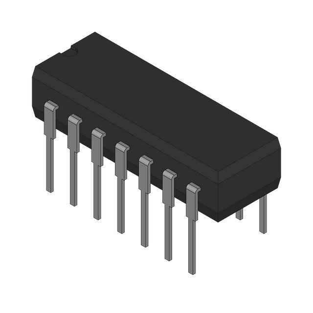
Figure 2. 14-Pin PDIP/SOIC – Top View
(See Package Number NFF0014A or D)
10:
Gain
Trim
191:
10k,
0.1%
9.95k
-
50:
CMRR
Trim
A1
10k, 0.1%
10k,
0.1%
-
VCM + 1/2VD
A2
VOUT = 100VD
+
VCM - 1/2VD
+
Figure 3. Low-Power Two-Op-Amp Instrumentation Amplifier
1
2
Please be aware that an important notice concerning availability, standard warranty, and use in critical applications of
Texas Instruments semiconductor products and disclaimers thereto appears at the end of this data sheet.
All trademarks are the property of their respective owners.
PRODUCTION DATA information is current as of publication date.
Products conform to specifications per the terms of the Texas
Instruments standard warranty. Production processing does not
necessarily include testing of all parameters.
Copyright © 1999–2013, Texas Instruments Incorporated
�LMC6462, LMC6464
SNOS725D – MAY 1999 – REVISED MARCH 2013
www.ti.com
These devices have limited built-in ESD protection. The leads should be shorted together or the device placed in conductive foam
during storage or handling to prevent electrostatic damage to the MOS gates.
Absolute Maximum Ratings (1) (2) (3)
ESD Tolerance (4)
2.0 kV
Differential Input Voltage
±Supply Voltage
(V+) + 0.3V, (V−) − 0.3V
Voltage at Input/Output Pin
−
+
Supply Voltage (V − V )
16V
Current at Input Pin (5)
±5 mA
Current at Output Pin (6) (7)
±30 mA
Current at Power Supply Pin
40 mA
Lead Temp. (Soldering, 10 sec.)
260°C
−65°C to +150°C
Storage Temperature Range
Junction Temperature (8)
(1)
(2)
(3)
(4)
(5)
(6)
(7)
(8)
150°C
Absolute Maximum Ratings indicate limits beyond which damage to the device may occur. Operating Ratings indicate conditions for
which the device is intended to be functional, but specific performance is not ensured. For ensured specifications and the test
conditions, see the Electrical Characteristics.
For specified Military Temperature Range parameters see RETSMC6462/4X.
If Military/Aerospace specified devices are required, please contact the Texas Instruments Sales Office/Distributors for availability and
specifications.
Human body model, 1.5 kΩ in series with 100 pF. All pins rated per method 3015.6 of MIL-STD-883. This is a class 2 device rating.
Limiting input pin current is only necessary for input voltages that exceed absolute maximum input voltage ratings.
Applies to both single supply and split-supply operation. Continuous short circuit operation at elevated ambient temperature can result in
exceeding the maximum allowed junction temperature of 150°C. Output currents in excess of ±30 mA over long term may adversely
affect reliability.
Do not short circuit output to V+, when V+ is greater than 13V or reliability will be adversely affected.
The maximum power dissipation is a function of TJ(MAX), θJA, and TA. The maximum allowable power dissipation at any ambient
temperature is PD = (TJ(MAX) − TA)/θJA. All numbers apply for packages soldered directly into a PC board.
Operating Ratings
3.0V ≤ V+ ≤ 15.5V
Supply Voltage
Junction Temperature
Range
Thermal Resistance (θJA)
−55°C ≤ TJ ≤ +125°C
LMC6462AM, LMC6464AM
LMC6462AI, LMC6464AI
−40°C ≤ TJ ≤ +85°C
LMC6462BI, LMC6464BI
−40°C ≤ TJ ≤ +85°C
P Package, 8-Pin PDIP
115°C/W
D Package, 8-Pin SOIC
193°C/W
NFF Package, 14-Pin PDIP
81°C/W
D Package, 14-Pin SOIC
(1)
126°C/W
Absolute Maximum Ratings indicate limits beyond which damage to the device may occur. Operating Ratings indicate conditions for
which the device is intended to be functional, but specific performance is not ensured. For ensured specifications and the test
conditions, see the Electrical Characteristics.
5V DC Electrical Characteristics
Unless otherwise specified, all limits ensured for TJ = 25°C, V+ = 5V, V− = 0V, VCM = VO = V+/2 and RL > 1M. Boldface limits
apply at the temperature extremes.
Typ (1)
Symbol
VOS
Parameter
Input Offset Voltage
TCVOS
Input Offset Voltage
Average Drift
IB
Input Current
(1)
(2)
(3)
2
Conditions
0.25
LMC6462AI
LMC6464AI
Limit (2)
LMC6462BI
LMC6464BI
Limit (2)
LMC6462AM
LMC6464AM
Limit (2)
0.5
3.0
0.5
mV
1.2
3.7
1.5
max
μV/°C
1.5
See (3)
0.15
Units
10
10
200
pA max
Typical Values represent the most likely parametric norm.
All limits are specified by testing or statistical analysis.
Specified limits are dictated by tester limitations and not device performance. Actual performance is reflected in the typical value.
Submit Documentation Feedback
Copyright © 1999–2013, Texas Instruments Incorporated
Product Folder Links: LMC6462 LMC6464
�LMC6462, LMC6464
www.ti.com
SNOS725D – MAY 1999 – REVISED MARCH 2013
5V DC Electrical Characteristics (continued)
Unless otherwise specified, all limits ensured for TJ = 25°C, V+ = 5V, V− = 0V, VCM = VO = V+/2 and RL > 1M. Boldface limits
apply at the temperature extremes.
Typ (1)
Symbol
Parameter
IOS
Input Offset Current
CIN
Common-Mode
Input Capacitance
RIN
Input Resistance
CMRR
Common Mode
Rejection Ratio
+PSRR
−PSRR
VCM
Conditions
See (3)
0.075
85
0V ≤ VCM ≤ 5.0V
V+ = 5V
85
Positive Power Supply
Rejection Ratio
5V ≤ V+ ≤ 15V,
V− = 0V, VO = 2.5V
85
Negative Power Supply
Rejection Ratio
−5V ≤ V− ≤ −15V,
V+ = 0V, VO = −2.5V
85
Input Common-Mode
Voltage Range
V+ = 5V
For CMRR ≥ 50 dB
−0.2
V+ = 15V
For CMRR ≥ 50 dB
−0.2
15.30
RL = 100 kΩ (4)
Sourcing
Sinking
RL = 25 kΩ (4)
Sourcing
Sinking
VO
Output Swing
Units
5
5
100
pA max
pF
Tera Ω
V+ = 5V
RL = 100 kΩ to V+/2
V+ = 5V
RL = 25 kΩ to V+/2
70
67
62
65
70
65
70
67
62
65
70
65
70
67
62
65
70
65
70
67
62
65
−0.10
−0.10
−0.10
0.00
0.00
0.00
5.25
5.25
5.25
5.00
5.00
5.00
−0.15
−0.15
−0.15
0.00
0.00
0.00
15.25
15.25
15.25
15.00
15.00
15.00
dB
min
dB
min
dB
min
V
max
V
min
V
max
V
min
400
V/mV
min
2500
V/mV
min
200
V/mV
min
4.995
4.990
14.990
0.010
V+ = 15V
RL = 25 kΩ to V+/2
65
V/mV
min
0.010
V+ = 15V
RL = 100 kΩ to V+/2
70
3000
0.005
14.965
0.025
(4)
LMC6462AM
LMC6464AM
Limit (2)
>10
0V ≤ VCM ≤ 15.0V,
V+ = 15V
Large Signal
Voltage Gain
LMC6462BI
LMC6464BI
Limit (2)
3
5.30
AV
LMC6462AI
LMC6464AI
Limit (2)
4.990
4.950
4.990
4.980
4.925
4.970
0.010
0.050
0.010
0.020
0.075
0.030
4.975
4.950
4.975
4.965
4.850
4.955
0.020
0.050
0.020
0.035
0.150
0.045
14.975
14.950
14.975
14.965
14.925
14.955
0.025
0.050
0.025
0.035
0.075
0.050
14.900
14.850
14.900
14.850
14.800
14.800
0.050
0.100
0.050
0.150
0.200
0.200
V
min
V
max
V
min
V
max
V
min
V
max
V
min
V
max
V+ = 15V, VCM = 7.5V and RL connected to 7.5V. For Sourcing tests, 7.5V ≤ VO ≤ 11.5V. For Sinking tests, 3.5V ≤ VO ≤ 7.5V.
Copyright © 1999–2013, Texas Instruments Incorporated
Product Folder Links: LMC6462 LMC6464
Submit Documentation Feedback
3
�LMC6462, LMC6464
SNOS725D – MAY 1999 – REVISED MARCH 2013
www.ti.com
5V DC Electrical Characteristics (continued)
Unless otherwise specified, all limits ensured for TJ = 25°C, V+ = 5V, V− = 0V, VCM = VO = V+/2 and RL > 1M. Boldface limits
apply at the temperature extremes.
Typ (1)
Symbol
ISC
Output Short Circuit
Current
V+ = 5V
ISC
Output Short Circuit
Current
V+ = 15V
IS
(5)
Parameter
Supply Current
Conditions
Sourcing, VO = 0V
LMC6462AI
LMC6464AI
Limit (2)
LMC6462BI
LMC6464BI
Limit (2)
LMC6462AM
LMC6464AM
Limit (2)
19
19
19
15
15
15
22
22
22
17
17
17
24
24
24
17
17
17
55
55
55
45
45
45
55
55
55
70
70
75
110
110
110
140
140
150
60
60
27
Sinking, VO = 5V
27
Sourcing, VO = 0V
38
Sinking, VO = 12V (5)
75
Dual, LMC6462
V+ = +5V, VO = V+/2
40
Quad, LMC6464
V+ = +5V, VO = V+/2
80
Dual, LMC6462
V+ = +15V, VO = V+/2
50
60
70
70
75
Quad, LMC6464
V+ = +15V, VO = V+/2
90
120
120
120
140
140
150
Units
mA
min
mA
min
mA
min
mA
min
μA
max
μA
max
μA
max
μA
max
Do not short circuit output to V+, when V+ is greater than 13V or reliability will be adversely affected.
5V AC Electrical Characteristics
Unless otherwise specified, all limits ensured for TJ = 25°C, V+ = 5V, V− = 0V, VCM = VO = V+/2 and RL > 1M. Boldface limits
apply at the temperature extremes.
Typ (1)
Symbol
SR
Parameter
Slew Rate
GBW
Gain-Bandwidth Product
φm
Gm
Conditions
See (3)
V+ = 15V
28
LMC6462AI
LMC6464AI
Limit (2)
LMC6462BI
LMC6464BI
Limit (2)
LMC6462AM
LMC6464AM
Limit (2)
15
15
15
8
8
8
Units
V/ms
min
50
kHz
Phase Margin
50
Deg
Gain Margin
15
dB
Amp-to-Amp Isolation
See (4)
130
dB
en
Input-Referred
Voltage Noise
f = 1 kHz
VCM = 1V
80
nV/√Hz
in
Input-Referred Current Noise
f = 1 kHz
0.03
pA/√Hz
(1)
(2)
(3)
(4)
4
Typical Values represent the most likely parametric norm.
All limits are specified by testing or statistical analysis.
V+ = 15V. Connected as Voltage Follower with 10V step input. Number specified is the slower of either the positive or negative slew
rates.
Input referred, V+ = 15V and RL = 100 kΩ connected to 7.5V. Each amp excited in turn with 1 kHz to produce VO = 12 VPP.
Submit Documentation Feedback
Copyright © 1999–2013, Texas Instruments Incorporated
Product Folder Links: LMC6462 LMC6464
�LMC6462, LMC6464
www.ti.com
SNOS725D – MAY 1999 – REVISED MARCH 2013
3V DC Electrical Characteristics
Unless otherwise specified, all limits ensured for TJ = 25°C, V+ = 3V, V− = 0V, VCM = VO = V+/2 and RL > 1M. Boldface limits
apply at the temperature extremes.
Typ (1)
Symbol
VOS
Parameter
Conditions
Input Offset Voltage
0.9
LMC6462AI
LMC6464AI
Limit (2)
LMC6462BI
LMC6464BI
Limit (2)
LMC6462AM
LMC6464AM
Limit (2)
2.0
3.0
2.0
2.7
3.7
3.0
Units
mV
max
TCVOS
Input Offset Voltage
Average Drift
IB
Input Current
See (3)
0.15
10
10
200
pA
IOS
Input Offset Current
See (3)
0.075
5
5
100
pA
CMRR
Common Mode
Rejection Ratio
0V ≤ VCM ≤ 3V
74
60
60
60
dB
min
PSRR
Power Supply
Rejection Ratio
3V ≤ V+ ≤ 15V, V− = 0V
80
60
60
60
dB
min
VCM
Input Common-Mode
Voltage Range
For CMRR ≥ 50 dB
−0.10
0.0
0.0
0.0
V
max
3.0
3.0
3.0
3.0
2.95
2.9
2.9
2.9
V
min
0.15
0.1
0.1
0.1
V
max
Dual, LMC6462
VO = V+/2
40
55
55
55
μA
70
70
70
Quad, LMC6464
VO = V+/2
80
110
110
110
140
140
140
VO
Output Swing
IS
(1)
(2)
(3)
Supply Current
μV/°C
2.0
RL = 25 kΩ to V+/2
V
min
μA
max
Typical Values represent the most likely parametric norm.
All limits are specified by testing or statistical analysis.
Specified limits are dictated by tester limitations and not device performance. Actual performance is reflected in the typical value.
3V AC Electrical Characteristics
Unless otherwise specified, V+ = 3V, V− = 0V, VCM = VO = V+/2 and RL > 1M. Boldface limits apply at the temperature
extremes.
Typ (1)
Symbol
Parameter
SR
Slew Rate
GBW
Gain-Bandwidth Product
(1)
(2)
(3)
Conditions
See (3)
LMC6462AI
LMC6464AI
Limit (2)
LMC6462BI
LMC6464BI
Limit (2)
LMC6462AM
LMC6464AM
Limit (2)
Units
23
V/ms
50
kHz
Typical Values represent the most likely parametric norm.
All limits are specified by testing or statistical analysis.
Connected as Voltage Follower with 2V step input. Number specified is the slower of either the positive or negative slew rates.
Copyright © 1999–2013, Texas Instruments Incorporated
Product Folder Links: LMC6462 LMC6464
Submit Documentation Feedback
5
�LMC6462, LMC6464
SNOS725D – MAY 1999 – REVISED MARCH 2013
www.ti.com
Typical Performance Characteristics
VS = +5V, Single Supply, TA = 25°C unless otherwise specified
6
Supply Current
vs.
Supply Voltage
Sourcing Current
vs.
Output Voltage
Figure 4.
Figure 5.
Sourcing Current
vs.
Output Voltage
Sourcing Current
vs.
Output Voltage
Figure 6.
Figure 7.
Sinking Current
vs.
Output Voltage
Sinking Current
vs.
Output Voltage
Figure 8.
Figure 9.
Submit Documentation Feedback
Copyright © 1999–2013, Texas Instruments Incorporated
Product Folder Links: LMC6462 LMC6464
�LMC6462, LMC6464
www.ti.com
SNOS725D – MAY 1999 – REVISED MARCH 2013
Typical Performance Characteristics (continued)
VS = +5V, Single Supply, TA = 25°C unless otherwise specified
Sinking Current
vs.
Output Voltage
Input Voltage Noise
vs
Frequency
Figure 10.
Figure 11.
Input Voltage Noise
vs.
Input Voltage
Input Voltage Noise
vs.
Input Voltage
Figure 12.
Figure 13.
Input Voltage Noise
vs.
Input Voltage
ΔVOS
vs
CMR
Figure 14.
Figure 15.
Copyright © 1999–2013, Texas Instruments Incorporated
Product Folder Links: LMC6462 LMC6464
Submit Documentation Feedback
7
�LMC6462, LMC6464
SNOS725D – MAY 1999 – REVISED MARCH 2013
www.ti.com
Typical Performance Characteristics (continued)
VS = +5V, Single Supply, TA = 25°C unless otherwise specified
8
Input Voltage
vs.
Output Voltage
Open Loop Frequency Response
Figure 16.
Figure 17.
Open Loop Frequency Response
vs.
Temperature
Gain and Phase
vs.
Capacitive Load
Figure 18.
Figure 19.
Slew Rate
vs.
Supply Voltage
Non-Inverting Large Signal Pulse Response
Figure 20.
Figure 21.
Submit Documentation Feedback
Copyright © 1999–2013, Texas Instruments Incorporated
Product Folder Links: LMC6462 LMC6464
�LMC6462, LMC6464
www.ti.com
SNOS725D – MAY 1999 – REVISED MARCH 2013
Typical Performance Characteristics (continued)
VS = +5V, Single Supply, TA = 25°C unless otherwise specified
Non-Inverting Large Signal Pulse Response
Non-Inverting Large Signal Pulse Response
Figure 22.
Figure 23.
Non-Inverting Small Signal Pulse Response
Non-Inverting Small Signal Pulse Response
Figure 24.
Figure 25.
Non-Inverting Small Signal Pulse Response
Inverting Large Signal Pulse Response
Figure 26.
Figure 27.
Copyright © 1999–2013, Texas Instruments Incorporated
Product Folder Links: LMC6462 LMC6464
Submit Documentation Feedback
9
�LMC6462, LMC6464
SNOS725D – MAY 1999 – REVISED MARCH 2013
www.ti.com
Typical Performance Characteristics (continued)
VS = +5V, Single Supply, TA = 25°C unless otherwise specified
Inverting Large Signal Pulse Response
Inverting Large Signal Pulse Response
Figure 28.
Figure 29.
Inverting Small Signal Pulse Response
Inverting Small Signal Pulse Response
Figure 30.
Figure 31.
Inverting Small Signal Pulse Response
Figure 32.
10
Submit Documentation Feedback
Copyright © 1999–2013, Texas Instruments Incorporated
Product Folder Links: LMC6462 LMC6464
�LMC6462, LMC6464
www.ti.com
SNOS725D – MAY 1999 – REVISED MARCH 2013
APPLICATION INFORMATION
Input Common-Mode Voltage Range
The LMC6462/4 has a rail-to-rail input common-mode voltage range. Figure 33 shows an input voltage
exceeding both supplies with no resulting phase inversion on the output.
Figure 33. An Input Voltage Signal Exceeds the LMC6462/4 Power Supply Voltage with No Output Phase
Inversion
The absolute maximum input voltage at V+ = 3V is 300 mV beyond either supply rail at room temperature.
Voltages greatly exceeding this absolute maximum rating, as in Figure 34, can cause excessive current to flow in
or out of the input pins, possibly affecting reliability. The input current can be externally limited to ±5 mA, with an
input resistor, as shown in Figure 35.
Copyright © 1999–2013, Texas Instruments Incorporated
Product Folder Links: LMC6462 LMC6464
Submit Documentation Feedback
11
�LMC6462, LMC6464
SNOS725D – MAY 1999 – REVISED MARCH 2013
www.ti.com
Figure 34. A ±7.5V Input Signal Greatly Exceeds the 3V Supply in Figure 35 Causing No Phase Inversion
Due to RI
Figure 35. Input Current Protection for Voltages Exceeding the Supply Voltage
Rail-to-Rail Output
The approximated output resistance of the LMC6462/4 is 180Ω sourcing, and 130Ω sinking at VS = 3V, and
110Ω sourcing and 83Ω sinking at VS = 5V. The maximum output swing can be estimated as a function of load
using the calculated output resistance.
Capacitive Load Tolerance
The LMC6462/4 can typically drive a 200 pF load with VS = 5V at unity gain without oscillating. The unity gain
follower is the most sensitive configuration to capacitive load. Direct capacitive loading reduces the phase margin
of op-amps. The combination of the op-amp's output impedance and the capacitive load induces phase lag. This
results in either an underdamped pulse response or oscillation.
Capacitive load compensation can be accomplished using resistive isolation as shown in Figure 36. If there is a
resistive component of the load in parallel to the capacitive component, the isolation resistor and the resistive
load create a voltage divider at the output. This introduces a DC error at the output.
12
Submit Documentation Feedback
Copyright © 1999–2013, Texas Instruments Incorporated
Product Folder Links: LMC6462 LMC6464
�LMC6462, LMC6464
www.ti.com
SNOS725D – MAY 1999 – REVISED MARCH 2013
Figure 36. Resistive Isolation of a 300 pF Capacitive Load
Figure 37. Pulse Response of the LMC6462 Circuit Shown in Figure 36
Figure 37 displays the pulse response of the LMC6462/4 circuit in Figure 36.
Another circuit, shown in Figure 38, is also used to indirectly drive capacitive loads. This circuit is an
improvement to the circuit shown in Figure 36 because it provides DC accuracy as well as AC stability. R1 and
C1 serve to counteract the loss of phase margin by feeding the high frequency component of the output signal
back to the amplifiers inverting input, thereby preserving phase margin in the overall feedback loop. The values
of R1 and C1 should be experimentally determined by the system designer for the desired pulse response.
Increased capacitive drive is possible by increasing the value of the capacitor in the feedback loop.
Copyright © 1999–2013, Texas Instruments Incorporated
Product Folder Links: LMC6462 LMC6464
Submit Documentation Feedback
13
�LMC6462, LMC6464
SNOS725D – MAY 1999 – REVISED MARCH 2013
www.ti.com
Figure 38. LMC6462 Non-Inverting Amplifier, Compensated to Handle a 300 pF Capacitive and 100 kΩ
Resistive Load
Figure 39. Pulse Response of LMC6462 Circuit in Figure 38
The pulse response of the circuit shown in Figure 38 is shown in Figure 39
Compensating for Input Capacitance
It is quite common to use large values of feedback resistance with amplifiers that have ultra-low input current,
like the LMC6462/4. Large feedback resistors can react with small values of input capacitance due to
transducers, photodiodes, and circuits board parasitics to reduce phase margins.
14
Submit Documentation Feedback
Copyright © 1999–2013, Texas Instruments Incorporated
Product Folder Links: LMC6462 LMC6464
�LMC6462, LMC6464
www.ti.com
SNOS725D – MAY 1999 – REVISED MARCH 2013
Figure 40. Canceling the Effect of Input Capacitance
The effect of input capacitance can be compensated for by adding a feedback capacitor. The feedback capacitor
(as in Figure 40 ), CF, is first estimated by:
(1)
or
R1 CIN ≤ R2 CF
(2)
which typically provides significant overcompensation.
Printed circuit board stray capacitance may be larger or smaller than that of a breadboard, so the actual optimum
value for CF may be different. The values of CF should be checked on the actual circuit. (Refer to the LMC660
quad CMOS amplifier data sheet for a more detailed discussion.)
Offset Voltage Adjustment
Offset voltage adjustment circuits are illustrated in Figure 41 and Figure 42. Large value resistances and
potentiometers are used to reduce power consumption while providing typically ±2.5 mV of adjustment range,
referred to the input, for both configurations with VS = ±5V.
Figure 41. Inverting Configuration Offset Voltage Adjustment
Figure 42. Non-Inverting Configuration Offset Voltage Adjustment
SPICE Macromodel
A Spice macromodel is available for the LMC6462/4. This model includes a simulation of:
• Input common-mode voltage range
Copyright © 1999–2013, Texas Instruments Incorporated
Product Folder Links: LMC6462 LMC6464
Submit Documentation Feedback
15
�LMC6462, LMC6464
SNOS725D – MAY 1999 – REVISED MARCH 2013
•
•
•
•
www.ti.com
Frequency and transient response
GBW dependence on loading conditions
Quiescent and dynamic supply current
Output swing dependence on loading conditions
and many more characteristics as listed on the macromodel disk.
Contact the Texas Instruments Customer Response Center to obtain an operational amplifier Spice model library
disk
Printed-Circuit-Board Layout for High-Impedance Work
It is generally recognized that any circuit which must operate with less than 1000 pA of leakage current requires
special layout of the PC board. When one wishes to take advantage of the ultra-low input current of the
LMC6462/4, typically 150 fA, it is essential to have an excellent layout. Fortunately, the techniques of obtaining
low leakages are quite simple. First, the user must not ignore the surface leakage of the PC board, even though
it may sometimes appear acceptably low, because under conditions of high humidity or dust or contamination,
the surface leakage will be appreciable.
To minimize the effect of any surface leakage, lay out a ring of foil completely surrounding the LMC6462's inputs
and the terminals of capacitors, diodes, conductors, resistors, relay terminals, etc. connected to the op-amp's
inputs, as in Figure 43. To have a significant effect, guard rings should be placed in both the top and bottom of
the PC board. This PC foil must then be connected to a voltage which is at the same voltage as the amplifier
inputs, since no leakage current can flow between two points at the same potential. For example, a PC board
trace-to-pad resistance of 1012Ω, which is normally considered a very large resistance, could leak 5 pA if the
trace were a 5V bus adjacent to the pad of the input. This would cause a 30 times degradation from the
LMC6462/4's actual performance. However, if a guard ring is held within 5 mV of the inputs, then even a
resistance of 1011Ω would cause only 0.05 pA of leakage current. See Figure 44 through Figure 46 for typical
connections of guard rings for standard op-amp configurations.
Figure 43. Example of Guard Ring in P.C. Board Layout
16
Submit Documentation Feedback
Copyright © 1999–2013, Texas Instruments Incorporated
Product Folder Links: LMC6462 LMC6464
�LMC6462, LMC6464
www.ti.com
SNOS725D – MAY 1999 – REVISED MARCH 2013
Figure 44. Typical Connections of Guard Rings – Inverting Amplifier
Figure 45. Typical Connections of Guard Rings – Non-Inverting Amplifier
Figure 46. Typical Connections of Guard Rings – Follower
The designer should be aware that when it is inappropriate to lay out a PC board for the sake of just a few
circuits, there is another technique which is even better than a guard ring on a PC board: Don't insert the
amplifier's input pin into the board at all, but bend it up in the air and use only air as an insulator. Air is an
excellent insulator. In this case you may have to forego some of the advantages of PC board construction, but
the advantages are sometimes well worth the effort of using point-to-point up-in-the-air wiring. See Figure 47.
(Input pins are lifted out of PC board and soldered directly to components. All other pins connected to PC board.)
Figure 47. Air Wiring
Instrumentation Circuits
The LMC6464 has the high input impedance, large common-mode range and high CMRR needed for designing
instrumentation circuits. Instrumentation circuits designed with the LMC6464 can reject a larger range of
common-mode signals than most in-amps. This makes instrumentation circuits designed with the LMC6464 an
excellent choice for noisy or industrial environments. Other applications that benefit from these features include
analytic medical instruments, magnetic field detectors, gas detectors, and silicon-based transducers.
Copyright © 1999–2013, Texas Instruments Incorporated
Product Folder Links: LMC6462 LMC6464
Submit Documentation Feedback
17
�LMC6462, LMC6464
SNOS725D – MAY 1999 – REVISED MARCH 2013
www.ti.com
A small valued potentiometer is used in series with RG to set the differential gain of the three op-amp
instrumentation circuit in Figure 48. This combination is used instead of one large valued potentiometer to
increase gain trim accuracy and reduce error due to vibration.
Figure 48. Low Power Three Op-Amp Instrumentation Amplifier
A two op-amp instrumentation amplifier designed for a gain of 100 is shown in Figure 49. Low sensitivity
trimming is made for offset voltage, CMRR and gain. Low cost and low power consumption are the main
advantages of this two op-amp circuit.
Higher frequency and larger common-mode range applications are best facilitated by a three op-amp
instrumentation amplifier.
10:
Gain
Trim
191:
10k,
0.1%
9.95k
-
50:
CMRR
Trim
A1
10k, 0.1%
10k,
0.1%
-
VCM + 1/2VD
A2
VOUT = 100VD
+
VCM - 1/2VD
+
Figure 49. Low-Power Two-Op-Amp Instrumentation Amplifier
18
Submit Documentation Feedback
Copyright © 1999–2013, Texas Instruments Incorporated
Product Folder Links: LMC6462 LMC6464
�LMC6462, LMC6464
www.ti.com
SNOS725D – MAY 1999 – REVISED MARCH 2013
TYPICAL SINGLE-SUPPLY APPLICATIONS
Transducer Interface Circuits
Figure 50. Photo Detector Circuit
Photocells can be used in portable light measuring instruments. The LMC6462, which can be operated off a
battery, is an excellent choice for this circuit because of its very low input current and offset voltage.
LMC6462 as a Comparator
Figure 51. Comparator with Hysteresis
Figure 51 shows the application of the LMC6462 as a comparator. The hysteresis is determined by the ratio of
the two resistors. The LMC6462 can thus be used as a micropower comparator, in applications where the
quiescent current is an important parameter.
Half-Wave and Full-Wave Rectifiers
Figure 52. Half-Wave Rectifier with Input Current Protection (RI)
Figure 53. Full-Wave Rectifier with Input Current Protection (RI)
Copyright © 1999–2013, Texas Instruments Incorporated
Product Folder Links: LMC6462 LMC6464
Submit Documentation Feedback
19
�LMC6462, LMC6464
SNOS725D – MAY 1999 – REVISED MARCH 2013
www.ti.com
In Figure 52 Figure 53, RI limits current into the amplifier since excess current can be caused by the input
voltage exceeding the supply voltage.
Precision Current Source
Figure 54. Precision Current Source
The output current IOUT is given by:
(3)
Oscillators
Figure 55. 1 Hz Square-Wave Oscillator
For single supply 5V operation, the output of the circuit will swing from 0V to 5V. The voltage divider set up R2,
R3 and R4 will cause the non-inverting input of the LMC6462 to move from 1.67V (⅓ of 5V) to 3.33V (⅔ of 5V).
This voltage behaves as the threshold voltage.
R1 and C1 determine the time constant of the circuit. The frequency of oscillation, fOSC is
(4)
where Δt is the time the amplifier input takes to move from 1.67V to 3.33V. The calculations are shown below.
(5)
where τ = RC = 0.68 seconds
→t1 = 0.27 seconds.
and
(6)
→t2 = 0.75 seconds
20
Submit Documentation Feedback
Copyright © 1999–2013, Texas Instruments Incorporated
Product Folder Links: LMC6462 LMC6464
�LMC6462, LMC6464
www.ti.com
SNOS725D – MAY 1999 – REVISED MARCH 2013
Then,
(7)
(8)
= 1 Hz
Low Frequency Null
Figure 56. High Gain Amplifier with Low Frequency Null
Output offset voltage is the error introduced in the output voltage due to the inherent input offset voltage VOS, of
an amplifier.
Output Offset Voltage = (Input Offset Voltage) (Gain)
In the above configuration, the resistors R5 and R6 determine the nominal voltage around which the input signal,
VIN should be symmetrical. The high frequency component of the input signal VIN will be unaffected while the low
frequency component will be nulled since the DC level of the output will be the input offset voltage of the
LMC6462 plus the bias voltage. This implies that the output offset voltage due to the top amplifier will be
eliminated.
Copyright © 1999–2013, Texas Instruments Incorporated
Product Folder Links: LMC6462 LMC6464
Submit Documentation Feedback
21
�LMC6462, LMC6464
SNOS725D – MAY 1999 – REVISED MARCH 2013
www.ti.com
REVISION HISTORY
Changes from Revision C (March 2013) to Revision D
•
22
Page
Changed layout of National Data Sheet to TI format .......................................................................................................... 21
Submit Documentation Feedback
Copyright © 1999–2013, Texas Instruments Incorporated
Product Folder Links: LMC6462 LMC6464
�PACKAGE OPTION ADDENDUM
www.ti.com
9-Sep-2022
PACKAGING INFORMATION
Orderable Device
Status
(1)
Package Type Package Pins Package
Drawing
Qty
Eco Plan
(2)
Lead finish/
Ball material
MSL Peak Temp
Op Temp (°C)
Device Marking
(3)
Samples
(4/5)
(6)
LMC6462AIM
NRND
SOIC
D
8
95
Non-RoHS
& Green
Call TI
Level-1-235C-UNLIM
-40 to 85
LMC64
62AIM
LMC6462AIM/NOPB
ACTIVE
SOIC
D
8
95
RoHS & Green
SN
Level-1-260C-UNLIM
-40 to 85
LMC64
62AIM
Samples
LMC6462AIMX/NOPB
ACTIVE
SOIC
D
8
2500
RoHS & Green
SN
Level-1-260C-UNLIM
-40 to 85
LMC64
62AIM
Samples
LMC6462AIN/NOPB
ACTIVE
PDIP
P
8
40
RoHS & Green
NIPDAU
Level-1-NA-UNLIM
-40 to 85
LMC6462
AIN
Samples
LMC6462BIM/NOPB
ACTIVE
SOIC
D
8
95
RoHS & Green
SN
Level-1-260C-UNLIM
-40 to 85
LMC64
62BIM
Samples
LMC6462BIMX/NOPB
ACTIVE
SOIC
D
8
2500
RoHS & Green
SN
Level-1-260C-UNLIM
-40 to 85
LMC64
62BIM
Samples
LMC6462BIN/NOPB
ACTIVE
PDIP
P
8
40
RoHS & Green
NIPDAU
Level-1-NA-UNLIM
-40 to 85
LMC6462
BIN
Samples
LMC6464AIM
NRND
SOIC
D
14
55
Non-RoHS
& Green
Call TI
Level-1-235C-UNLIM
-40 to 85
LMC6464
AIM
LMC6464AIM/NOPB
ACTIVE
SOIC
D
14
55
RoHS & Green
SN
Level-1-260C-UNLIM
-40 to 85
LMC6464
AIM
LMC6464AIMX
NRND
SOIC
D
14
2500
Non-RoHS
& Green
Call TI
Level-1-235C-UNLIM
-40 to 85
LMC6464
AIM
LMC6464AIMX/NOPB
ACTIVE
SOIC
D
14
2500
RoHS & Green
SN
Level-1-260C-UNLIM
-40 to 85
LMC6464
AIM
Samples
LMC6464BIM/NOPB
ACTIVE
SOIC
D
14
55
RoHS & Green
SN
Level-1-260C-UNLIM
-40 to 85
LMC6464
BIM
Samples
LMC6464BIMX/NOPB
ACTIVE
SOIC
D
14
2500
RoHS & Green
SN
Level-1-260C-UNLIM
-40 to 85
LMC6464
BIM
Samples
LMC6464BIN/NOPB
ACTIVE
PDIP
N
14
25
RoHS & Green
NIPDAU
Level-1-NA-UNLIM
-40 to 85
LMC6464BIN
Samples
(1)
The marketing status values are defined as follows:
ACTIVE: Product device recommended for new designs.
LIFEBUY: TI has announced that the device will be discontinued, and a lifetime-buy period is in effect.
NRND: Not recommended for new designs. Device is in production to support existing customers, but TI does not recommend using this part in a new design.
PREVIEW: Device has been announced but is not in production. Samples may or may not be available.
OBSOLETE: TI has discontinued the production of the device.
Addendum-Page 1
Samples
�PACKAGE OPTION ADDENDUM
www.ti.com
9-Sep-2022
(2)
RoHS: TI defines "RoHS" to mean semiconductor products that are compliant with the current EU RoHS requirements for all 10 RoHS substances, including the requirement that RoHS substance
do not exceed 0.1% by weight in homogeneous materials. Where designed to be soldered at high temperatures, "RoHS" products are suitable for use in specified lead-free processes. TI may
reference these types of products as "Pb-Free".
RoHS Exempt: TI defines "RoHS Exempt" to mean products that contain lead but are compliant with EU RoHS pursuant to a specific EU RoHS exemption.
Green: TI defines "Green" to mean the content of Chlorine (Cl) and Bromine (Br) based flame retardants meet JS709B low halogen requirements of


 工商网监
湘ICP备2023018690号
工商网监
湘ICP备2023018690号
