������ ������ ������
�
��
�
���� �����
������ � ���
��
�
The LP239 is obsolete
and is no longer supplied.
SLCS004B − OCTOBER 1987 − REVISED SEPTEMBER 2004
D Wide Supply-Voltage Range . . . 3 V to 30 V
D Ultralow Power Supply Current
D
D
D
D
D
D
D
D
D
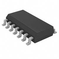
D OR N PACKAGE
(TOP VIEW)
Drain . . . 60 µA Typ
Low Input Biasing Current . . . 3 nA
Low Input Offset Current . . . ±0.5 nA
Low Input Offset Voltage . . . ±2 mV
Common-Mode Input Voltage Includes
Ground
Output Voltage Compatible With MOS and
CMOS Logic
High Output Sink-Current Capability
(30 mA at VO = 2V)
Power Supply Input Reverse-Voltage
Protected
Single-Power-Supply Operation
Pin-for-Pin Compatible With LM239, LM339,
LM2901
1OUT
2OUT
VCC
2IN −
2IN +
1IN −
1IN +
1
14
2
13
3
12
4
11
5
10
6
9
7
8
3OUT
4OUT
GND
4IN +
4IN −
3IN +
3IN −
description/ordering information
The LP239, LP339, LP2901 are low-power quadruple differential comparators. Each device consists of four
independent voltage comparators designed specifically to operate from a single power supply and typically to
draw 60-µA drain current over a wide range of voltages. Operation from split power supplies also is possible
and the ultra-low power-supply drain current is independent of the power-supply voltage.
Applications include limit comparators, simple analog-to-digital converters, pulse generators, squarewave
generators, time-delay generators, voltage-controlled oscillators, multivibrators, and high-voltage logic gates.
The LP239, LP339, LP2901 were designed specifically to interface with the CMOS logic family. The ultra-low
power-supply current makes these products desirable in battery-powered applications.
The LP239 is characterized for operation from −25°C to 85°C. The LP339 is characterized for operation from
0°C to 70°C. The LP2901 is characterized for operation from −40°C to 85°C.
ORDERING INFORMATION
TA
VIOMAX
AT 25°C
PDIP (N)
0°C
0
C to 70
70°C
C
± 5 mV
SOIC (D)
PDIP (N)
−40°C
−40
C to 85
85°C
C
± 5 mV
ORDERABLE
PART NUMBER
PACKAGE†
SOIC (D)
Tube of 25
LP339N
Tube of 50
LP339D
Reel of 2500
LP339DR
Tube of 25
LP2901N
Tube of 50
LP2901D
Reel of 2500
LP2901DR
TOP-SIDE
MARKING
LP339N
LP339
LP2901N
LP2901
† Package drawings, standard packing quantities, thermal data, symbolization, and PCB design guidelines are available at
www.ti.com/sc/package.
Please be aware that an important notice concerning availability, standard warranty, and use in critical applications of
Texas Instruments semiconductor products and disclaimers thereto appears at the end of this data sheet.
Copyright 2004, Texas Instruments Incorporated
�
����� � ���� �������!��� �" #$��%�! �" �� &$'(�#�!��� )�!%*
���)$#!" #������ !� "&%#���#�!���" &%� !+% !%��" �� �%,�" ��"!�$�%�!"
"!��)��) -�����!.* ���)$#!��� &��#%""��/ )�%" ��! �%#%""���(. ��#($)%
!%"!��/ �� �(( &����%!%�"*
POST OFFICE BOX 655303
• DALLAS, TEXAS 75265
1
������� ������ ������
�
��
�
���� �����
������ � ���
��
�
The LP239 is obsolete
and is no longer supplied.
SLCS004B − OCTOBER 1987 − REVISED SEPTEMBER 2004
schematic diagram (each comparator)
VCC
0.2 µA
5 µA
6 µA
0.2 µA
IN+
OUT
IN−
GND
absolute maximum ratings over operating free-air temperature range (unless otherwise noted)†
Supply voltage, VCC (see Note 1) . . . . . . . . . . . . . . . . . . . . . . . . . . . . . . . . . . . . . . . . . . . . . . . . . . . . . . . . . . . . 36 V
Differential input voltage, VID (see Note 2) . . . . . . . . . . . . . . . . . . . . . . . . . . . . . . . . . . . . . . . . . . . . . . . . . . . ±36 V
Input voltage range, VI (either input) . . . . . . . . . . . . . . . . . . . . . . . . . . . . . . . . . . . . . . . . . . . . . . . . . −0.3 V to 36 V
Input current, VI ≤ −0.3 V (see Note 3) . . . . . . . . . . . . . . . . . . . . . . . . . . . . . . . . . . . . . . . . . . . . . . . . . . . . . −50 mA
Duration of output short-circuit to ground (see Note 4) . . . . . . . . . . . . . . . . . . . . . . . . . . . . . . . . . . . . . . Unlimited
Continuous total dissipation (see Note 5) . . . . . . . . . . . . . . . . . . . . . . . . . . . . . . . . See Dissipation Rating Table
Operating free-air temperature range, TA: LP239 . . . . . . . . . . . . . . . . . . . . . . . . . . . . . . . . . . . . . . −25°C to 85°C
LP339 . . . . . . . . . . . . . . . . . . . . . . . . . . . . . . . . . . . . . . . . 0°C to 70°C
LP2901 . . . . . . . . . . . . . . . . . . . . . . . . . . . . . . . . . . . . . −40°C to 85°C
Package thermal impedance, θJA (see Notes 6 and 7): D package . . . . . . . . . . . . . . . . . . . . . . . . . . . . 86°C/W
N package . . . . . . . . . . . . . . . . . . . . . . . . . . . . 80°C/W
Operating virtual junction temperature, TJ . . . . . . . . . . . . . . . . . . . . . . . . . . . . . . . . . . . . . . . . . . . . . . . . . . . 150°C
Lead temperature range 1,6 mm (1/16 inch) from case for 60 seconds: J package . . . . . . . . . . . . . . . . 300°C
Storage temperature range, Tstg . . . . . . . . . . . . . . . . . . . . . . . . . . . . . . . . . . . . . . . . . . . . . . . . . . . −65°C to 150°C
† Stresses beyond those listed under absolute maximum ratings may cause permanent damage to the device. These are stress ratings only, and
functional operation of the device at these or any other conditions beyond those indicated in the recommended operating conditions is not implied.
Exposure to absolute-maximum-rated conditions for extended periods may affect device reliability.
NOTES: 1. All voltage values, except differential voltages, are with respect to the network ground.
2. Differential voltages are at IN+ with respect to IN −.
3. This input current only exists when the voltage at any of the inputs is driven negative. The current flows through the collector-base
junction of the input clamping device. In addition to the clamping device action, there is lateral n-p-n parasitic transistor action. This
action is not destructive, and normal output states are reestablished when the input voltage returns to a value more positive than
− 0.3 V at TA = 25°C.
4. Short circuits between outputs to VCC can cause excessive heating and eventual destruction.
5. If the output transistors are allowed to saturate, the low-bias dissipation and the on-off characteristics of the outputs keep the
dissipation very small (usually less than 100 mW).
6. Maximum power dissipation is a function of TJ(max), θJA, and TA. The maximum allowable power dissipation at any allowable
ambient temperature is PD = (TJ(max) − TA)/θJA. Operating at the absolute maximum TJ of 150°C can impact reliability.
7. The package thermal impedance is calculated in accordance with JESD 51-7.
DISSIPATION RATING TABLE
PACKAGE
J
2
TA ≤ 25°C
POWER RATING
1025 mW
DERATING FACTOR
ABOVE TA = 25°C
TA = 70°C
POWER RATING
TA = 85°C
POWER RATING
8.2 mW/°C
656 mW
533 mW
POST OFFICE BOX 655303
• DALLAS, TEXAS 75265
������� ������ ������
�
��
�
���� �����
������ � ���
��
�
The LP239 is obsolete
and is no longer supplied.
SLCS004B − OCTOBER 1987 − REVISED SEPTEMBER 2004
recommended operating conditions
LP239
VCC
LP339
LP2901
MIN
MAX
MIN
MAX
MIN
MAX
3
30
3
30
3
30
V
0
3
0
3
0
3
V
Common-mode input voltage
VCC = 5 V
VCC = 30 V
0
28
0
28
0
28
V
0
3
0
3
0
3
V
VI
Input voltage
VCC = 5 V
VCC = 30 V
0
28
0
28
0
28
V
TA
Operating free-air temperature
−25
85
0
70
−40
85
°C
VIC
Supply voltage
UNIT
electrical characteristics, VCC = 5 V, TA = 25°C (unless otherwise noted)
PARAMETER
VIO
Input offset voltage
IIO
Input offset current
IIB
Input bias current
TEST CONDITIONS
VCC = 5 V to 30 V,
RS = 0,
VO = 2 V,
See Note 6
TA†
25°C
MIN
±0.5
±5
±1
±15
−2.5
−25
−4
−40
Full range
See Note 7
Common-mode input voltage
range
Single supply
Large-signal differential voltage
amplification
VCC = 15 V,
Output sink current
VI− = 1 V,
VI+ = 0
Output leakage current
±5
±9
25°C
AVD
MAX
±2
Full range
25°C
VICR
TYP
VI+ = 1 V,
VI− = 0
Full range
25°C
0 to
VCC − 1.5
Full range
0 to
VCC − 2
VO = 0.4 V
VO = 5 V
VO = 30 V
VI ≤ 0 (or VCC − on split supplies)
500
25°C
20
Full range
15
25°C
0.2
mV
nA
nA
V
RL = 15 kΩ
VO = 2 V,
See Note 8
UNIT
V/mV
30
mA
0.7
25°C
0.1
Full range
nA
1
µA
VID
Differential input voltage
36
V
ICC
Supply current
RL = ∞ all comparators
60
100
µA
† Full range is −25°C to 85°C for the LP239, 0°C to 70°C for the LP339, and − 40°C to 85°C for the LP2901.
NOTES: 8. VIO is measured over the full common-mode input voltage range.
9. Because of the p-n-p input stage, the direction of the current is out of the device. This current essentially is constant (i.e., independent
of the output state). No loading change exists on the reference or input lines as long as the common-mode input voltage range is
not exceeded.
10. The output sink current is a function of the output voltage. These devices have a bimodal output section that allows them to sink
(via a Darlington connection) large currents at output voltages greater than 1.5 V, and smaller currents at output voltages
less than 1.5 V.
switching characteristics, VCC = 5 V, TA = 25°C, RL connected to 5 V through 5.1 kΩ
PARAMETER
Large-signal response time
Response time
TEST CONDITIONS
TTL logic swing, Vref = 1.4 V
POST OFFICE BOX 655303
• DALLAS, TEXAS 75265
MIN
TYP
1.3
8
MAX
UNIT
µs
3
������� ������ ������
�
��
�
���� �����
������ � ���
��
�
SLCS004B − OCTOBER 1987 − REVISED SEPTEMBER 2004
The LP239 is obsolete
and is no longer supplied.
APPLICATION INFORMATION
Figure 1 shows the basic configuration for using the LP239, LP339, or LP2901 comparator. Figure 2 shows the
diagram for using one of these comparators as a CMOS driver.
VCC
VCC
30 kΩ
IN +
100 kΩ
+
IN +
+
IN −
−
3
OUT
OUT
IN −
−
1/4 LP239, LP339,
or LP2901
12
1/4 LP239, LP339,
or LP2901
Figure 1. Basic Comparator
1/4 SN54/74LS00 or
1/4 SN54/74ALS1000A
Figure 2. CMOS Driver
All pins of any unused comparators should be grounded. The bias network of the LP239, LP339, and LP2901
establishes a drain current that is independent of the magnitude of the power-supply voltage over the range of
2 V to 30 V. It usually is necessary to use a bypass capacitor across the power supply line.
The differential input voltage may be larger than VCC without damaging the device. Protection should be
provided to prevent the input voltages from going negative by more than −0.3 V. The output section has two
distinct modes of operation: a Darlington mode and ground-emitter mode. This unique drive circuit permits the
device to sink 30 mA at VO = 2 V in the Darlington mode and 700 µA at VO = 0.4 V in the ground-emitter mode.
Figure 3 is a simplified schematic diagram of the output section. The output section is configured in a Darlington
connection (ignoring Q3). If the output voltage is held high enough (above 1 V), Q1 is not saturated and the
output current is limited only by the product of the hFE of Q1, the hFE of Q2, and I1 and the 60-Ω saturation
resistance of Q2. The devices are capable of driving LEDs, relays, etc. in this mode while maintaining an
ultra-low power-supply current of 60 µA, typically.
VCC
I1 = 6 µA
Q3
VO
Q1
Q2
Figure 3. Output-Section Schematic Diagram
4
POST OFFICE BOX 655303
• DALLAS, TEXAS 75265
�The LP239 is obsolete
and is no longer supplied.
������ ������ ������
�
��
�
���� �����
������ � ���
��
�
SLCS004B − OCTOBER 1987 − REVISED SEPTEMBER 2004
APPLICATION INFORMATION
Without transistor Q3, if the output voltage were allowed to drop below 0.8 V, transistor Q1 would saturate, and
the output current would drop to zero. The circuit would be unable to pull low current loads down to ground or
the negative supply, if used. Transistor Q3 has been included to bypass transistor Q1 under these conditions
and apply the current I1 directly to the base of Q2. The output sink current now is approximately I1 times the
hFE of Q2 (700 µA at VO = 0.4 V). The output of the devices exhibits a bimodal characteristic, with a smooth
transition between modes.
In both cases, the output is an uncommitted collector. Several outputs can be tied together to provide a dot logic
function. An output pullup resistor can be connected to any available power-supply voltage within the permitted
power-supply range, and there is no restriction on this voltage, based on the magnitude of the voltage that is
supplied to VCC of the package.
POST OFFICE BOX 655303
• DALLAS, TEXAS 75265
5
�PACKAGE OPTION ADDENDUM
www.ti.com
13-Jul-2022
PACKAGING INFORMATION
Orderable Device
Status
(1)
Package Type Package Pins Package
Drawing
Qty
Eco Plan
(2)
Lead finish/
Ball material
MSL Peak Temp
Op Temp (°C)
Device Marking
(3)
Samples
(4/5)
(6)
LP2901D
ACTIVE
SOIC
D
14
50
RoHS & Green
NIPDAU
Level-1-260C-UNLIM
-40 to 85
LP2901
Samples
LP2901DR
ACTIVE
SOIC
D
14
2500
RoHS & Green
NIPDAU
Level-1-260C-UNLIM
-40 to 85
LP2901
Samples
LP2901DRE4
ACTIVE
SOIC
D
14
2500
RoHS & Green
NIPDAU
Level-1-260C-UNLIM
-40 to 85
LP2901
Samples
LP2901DRG4
ACTIVE
SOIC
D
14
2500
RoHS & Green
NIPDAU
Level-1-260C-UNLIM
-40 to 85
LP2901
Samples
LP2901N
ACTIVE
PDIP
N
14
25
RoHS & Green
NIPDAU
N / A for Pkg Type
-40 to 85
LP2901N
Samples
LP339D
ACTIVE
SOIC
D
14
50
RoHS & Green
NIPDAU
Level-1-260C-UNLIM
0 to 70
LP339
Samples
LP339DG4
ACTIVE
SOIC
D
14
50
RoHS & Green
NIPDAU
Level-1-260C-UNLIM
0 to 70
LP339
Samples
LP339DR
ACTIVE
SOIC
D
14
2500
RoHS & Green
NIPDAU | SN
Level-1-260C-UNLIM
0 to 70
LP339
Samples
LP339DRE4
ACTIVE
SOIC
D
14
2500
RoHS & Green
NIPDAU
Level-1-260C-UNLIM
0 to 70
LP339
Samples
LP339DRG4
ACTIVE
SOIC
D
14
2500
RoHS & Green
NIPDAU
Level-1-260C-UNLIM
0 to 70
LP339
Samples
LP339N
ACTIVE
PDIP
N
14
25
RoHS & Green
NIPDAU
N / A for Pkg Type
0 to 70
LP339N
Samples
(1)
The marketing status values are defined as follows:
ACTIVE: Product device recommended for new designs.
LIFEBUY: TI has announced that the device will be discontinued, and a lifetime-buy period is in effect.
NRND: Not recommended for new designs. Device is in production to support existing customers, but TI does not recommend using this part in a new design.
PREVIEW: Device has been announced but is not in production. Samples may or may not be available.
OBSOLETE: TI has discontinued the production of the device.
(2)
RoHS: TI defines "RoHS" to mean semiconductor products that are compliant with the current EU RoHS requirements for all 10 RoHS substances, including the requirement that RoHS substance
do not exceed 0.1% by weight in homogeneous materials. Where designed to be soldered at high temperatures, "RoHS" products are suitable for use in specified lead-free processes. TI may
reference these types of products as "Pb-Free".
RoHS Exempt: TI defines "RoHS Exempt" to mean products that contain lead but are compliant with EU RoHS pursuant to a specific EU RoHS exemption.
Green: TI defines "Green" to mean the content of Chlorine (Cl) and Bromine (Br) based flame retardants meet JS709B low halogen requirements of


 工商网监
湘ICP备2023018690号
工商网监
湘ICP备2023018690号
