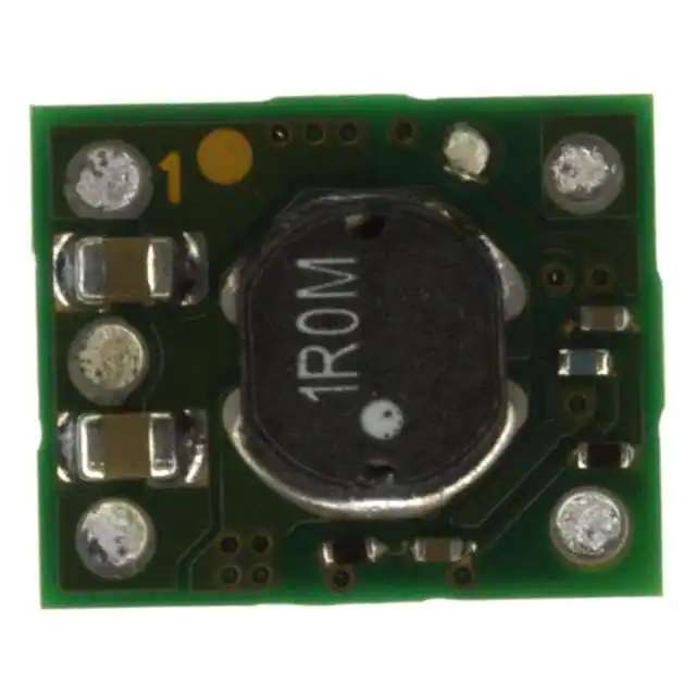
PTH04070W
www.ti.com
SLTS227B – SEPTEMBER 2004 – REVISED OCTOBER 2007
3-A, 3.3/5-V INPUT ADJUSTABLE SWITCHING REGULATOR
•
•
FEATURES
1
•
•
•
•
•
•
•
•
•
•
Up to 3-A Output Current at 85°C
3.3-V / 5-V Input Voltage
Wide-Output Voltage Adjust
(0.9 V to 3.6 V)
160 W/in3 Power Density
Efficiencies Up To 94%
On/Off Inhibit
Undervoltage Lockout (UVLO)
Output Overcurrent Protection
(Nonlatching, Auto-Reset)
Overtemperature Protection
Ambient Temp. Range: –40°C to 85°C
Surface Mount Package
Safety Agency Approvals:
UL/IEC/CSA-C22.2 60950-1
APPLICATIONS
•
Telecommunications, Instumentation,
and General-Purpose Circuits
DESCRIPTION
The PTH04070W is a highly integrated, low-cost switching regulator module that delivers up to 3 A of output
current. Occupying less PCB area than a standard TO-220 linear regulator IC, the PTH04070W provides output
current at a much higher efficiency and with much less power dissipation, thereby eliminating the need for a heat
sink. Their small size (0.5 × 0.4 in), high efficiency, and low cost makes these modules attractive for a variety of
applications.
The input voltage range of the PTH04070W is from 3 V to 5.5 V, allowing operation from either a 3.3-V or 5-V
input bus. Using state-of-the-art switched-mode power-conversion technology, the PTH04070W can step down to
voltages as low as 0.9 V from a 5-V input bus, with typically less than 1 W of power dissipation. The output
voltage can be adjusted to any voltage over the range, 0.9 V to 3.6 V, using a single external resistor. Operating
features include an undervoltage lockout (UVLO), on/off inhibit, output overcurrent protection, and
overtemperature protection. Target applications include telecommunications, test and measurement applications,
and high-end consumer products. The modules are available in both through-hole and surface-mount package
options, including tape and reel.
STANDARD APPLICATION
Inhibit
5
4
RSET
0.05 W#, 1%
(Required)
VI
VO
PTH04070W
(Top View)
1
3
2
GND
C1*
47 mF
Ceramic
(Required)
C2*
47 mF
Ceramic
(Required)
C3*
47 mF
Electroytic
(Recommended)
GND
#See The Specification Table for Value
*See The Capacitor Application Information
1
Please be aware that an important notice concerning availability, standard warranty, and use in critical applications of
Texas Instruments semiconductor products and disclaimers thereto appears at the end of this data sheet.
PRODUCTION DATA information is current as of publication date.
Products conform to specifications per the terms of the Texas
Instruments standard warranty. Production processing does not
necessarily include testing of all parameters.
Copyright © 2004–2007, Texas Instruments Incorporated
�PTH04070W
www.ti.com
SLTS227B – SEPTEMBER 2004 – REVISED OCTOBER 2007
These devices have limited built-in ESD protection. The leads should be shorted together or the device placed in conductive foam
during storage or handling to prevent electrostatic damage to the MOS gates.
ORDERING INFORMATION
For the most current package and ordering information, see the Package Option Addendum at the end of this datasheet, or see
the TI website at www.ti.com.
ABSOLUTE MAXIMUM RATINGS
over operating free-air temperature range unless otherwise noted (1)
PTH04070
TA
Operating free-air
temperature
Over VI range
Twave
Wave solder
temperature
Surface temperature of module body or pins
(5 seconds maximum)
Suffix AH & AD
Treflow
Solder reflow
temperature
Surface temperature of module body or pins
Suffix AS
235 (2)
Suffix AZ
260 (2)
Tstg
(1)
(2)
(3)
UNIT
-40 to 85
260
°C
-55 to 125 (3)
Storage temperature
Stresses beyond those listed under absolute maximum ratings may cause permanent damage to the device. These are stress ratings
only, and functional operation of the device at these or any other conditions beyond those indicated under recommended operating
conditions is not implied. Exposure to absolute-maximum-rated conditions for extended periods may affect device reliability.
During reflow of surface mount package version do not elevate peak temperature of the module, pins or internal components above the
stated maximum.
The shipping tray or tape and reel cannot be used to bake parts at temperatures higher than 65°C.
RECOMMENDED OPERATING CONDITIONS
VI
Input voltage
TA
Operating free-air temperature
MIN
MAX
3
5.5
UNIT
V
–40
85
°C
PACKAGE SPECIFICATIONS
PTH04070WXX
Weight
Flammability
Mechanical shock
Mechanical vibration
(1)
2
1.5 grams
Meets UL 94 V-O
Per Mil-STD-883D, Method 2002.3, 1 msec, 1/2 sine,
mounted
500 G
Mil-STD-883D, Method 2007.2, 20-2000 Hz
20 G
(1)
(1)
Qualification limit.
Submit Documentation Feedback
Copyright © 2004–2007, Texas Instruments Incorporated
Product Folder Link(s): PTH04070W
�PTH04070W
www.ti.com
SLTS227B – SEPTEMBER 2004 – REVISED OCTOBER 2007
ELECTRICAL CHARACTERISTICS
at 25C free-air temperature, VI = 5 V, VO = 3.3 V, IO = IO(Max), C1 = 47 μF, C2 = 47 μF (unless otherwise noted)
PARAMETER
TEST CONDITIONS
MIN
TYP
MAX
UNIT
IO
Output current
TA = 85°C, natural convection airflow
0
3
VI
Input voltage range
Over IO range
3
5.5
VO(tol)
Set-point voltage tolerance
TA = 25°C
Temperature variation
-40 ≤ TA ≤ +85°C
±0.5
%VO
Line regulation
Over VI range
±1
mV
Load regulation
Over IO range
±5
Total output voltage variation
Includes set-point, line, load,
–40 ≤ TA ≤ +85°C
VO(adj)
Output voltage adjust range
±2
(1)
A
V
%VO
mV
±3
(1)
VI ≥ 4.5 V
0.9
3.6
VI < 4.5 V
0.9
VI – 1.1 (2)
%VO
V
TA = 25°C, IO = 2 A
(2)
RSET = 475 Ω, VO = 3.3 V
RSET = 2.32 kΩ, VO = 2.5 V V
η
Efficiency
IO(trip)
92%
(2)
90%
RSET = 4.87 kΩ, VO = 2 V
88%
RSET = 6.65 kΩ, VO = 1.8 V
87%
RSET = 11.5 kΩ, VO = 1.5 V
85%
RSET = 26.1 kΩ, VO = 1.2 V
82%
RSET = 84.5 kΩ, VO = 1 V
80%
Output voltage ripple
20 MHz bandwith
Overcurrent threshold
Reset, followed by autorecovery
10
mVPP
7
A
C3 = 47 μF, 1 A/μs load step from 50% to
100% IOmax
Transient response
UVLO
Undervoltage lockout
Recovery time
70
μs
VO over/undershoot
100
mV
VI = increasing
VI = decreasing
Input high voltage (VIH)
Inhibit control (pin 5)
Input low voltage (VIL)
2.95
2.7
VI – 0.5
Input low current (IIL)
Input standby current
Pin 5 connected to GND
FS
Switching frequency
Over VI and IO ranges
External input capacitance
Ceramic type (C1)
47
(4)
Ceramic type (C2)
47
(5)
External output capacitance
Nonceramic type (C3)
Equivalent series resistance (nonceramic)
MTBF
(1)
(2)
(3)
(4)
(5)
(6)
(7)
Calculated reliability
Per Bellcore TR-332, 50% stress,
TA = 40°C, ground benign
Open
–0.2
II(stby)
V
(3)
0.6
V
–10
μA
1
mA
700
kHz
μF
200
47
4
3
2.8
(5)
560
(6)
μF
(7)
mΩ
48
106 Hrs
The set-point voltage tolerance is affected by the tolerance and stability of RSET. The stated limit is unconditionally met if RSET has a
tolerance of 1% with with 100 ppm/°C or better temperature stability.
The minimum input voltage is 3 V or (VO + 1.1) V, whichever is greater. A 5-V input bus is recommended for output voltages higher than
2 V.
This control pin has an internal pullup to the input voltage VI. If it is left open circuit, the module operates when input power is applied. A
small low-leakage ( 412
7.3L×4.3W
×4.1H
1
1
≤5
≤5
TPSD476M010R0100
TPSB476M010R0500
Kemet T520 (SMD)
AO-CAP
10
6.3
68
47
0.060
0.028
>1200
>1100
7.3L×5.7W
×4.0H
1
1
≤5
≤3
T520V686M010ASE060
A700V476M006AT
Vishay/Sprague 594D/595D
(SMD)
10
10
68
68
0.100
0.240
>1000
680
7.3L×6.0W
×4.1H
1
1
≤5
≤5
594D686X0010C2T
595D686X0010C2T
94SL
16
47
0.070
1550
8×5
1
≤5
94SL476X0016EBP
TDK Ceramic X5R
Murata Ceramic X5R
Kemet
6.3
6.3
6.3
22
22
22
0.002
0.002
0.002
>1400
>1000
>1000
1210 case
3225 mm
≥ 2 (3)
≥ 2 (3)
≥ 2 (3)
≤3
≤3
≤3
C3225X5R0J226KT/MT
GRM32ER61J223M
C1210C226K9PAC
TDK Ceramic X5R
Murata Ceramic X5R
Kemet
6.3
6.3
6.3
47
47
47
0.002
0.002
0.002
>1400
>1000
>1000
1210 case
3225 mm
≥1
≥1
≥1
≤3
≤3
≤3
C3225X5R0J476KT/MT
GRM32ER60J476M/6.3
C1210C476K9PAC
CAPACITOR VENDOR/
COMPONENT
SERIES
(1)
(2)
(3)
10
PHYSICAL
SIZE
(mm)
INPUT
BUS (1)
OUTPUT
BUS
VENDOR
NUMBER
EEFWA1A121P (2)
EEVFC1E470P (2)
A ceramic capacitor is required on both the input and the output. An electrolytic capacitor can be added to the output for improved
transient response.
An optional through-hole capacitor available.
A total capacitance of 44 μF is an acceptable replacement for a single 47-μF capacitor.
Submit Documentation Feedback
Copyright © 2004–2007, Texas Instruments Incorporated
Product Folder Link(s): PTH04070W
�PTH04070W
www.ti.com
SLTS227B – SEPTEMBER 2004 – REVISED OCTOBER 2007
Power-Up Characteristics
When configured per the standard application, the PTH04070W power module produces a regulated output
voltage following the application of a valid input source voltage. During power up, internal soft-start circuitry slows
the rate that the output voltage rises, thereby limiting the amount of in-rush current that can be drawn from the
input source. The soft-start circuitry introduces a short time delay (typically 10 ms) into the power-up
characteristic. This is from the point that a valid input source is recognized. Figure 10 shows the power-up
waveforms for a PTH04070W, operating from a 3-V input and with the output voltage adjusted to 1.8 V. The
waveforms were measured with a 2-A resistive load.
VI (1 V/div)
VO (1 V/div)
II (1 A/div)
t − 10 ms/div
Figure 10. Power-Up Waveforms
Current Limit Protection
The PTH04070W modules protect against load faults with a continuous current limit characteristic. Under a load
fault condition, the output current cannot exceed the current limit value. Attempting to draw current that exceeds
the current limit value causes the output voltage to be progressively reduced. Current is continuously supplied to
the fault until it is removed. Upon removal of the fault, the output voltage will promptly recover.
Thermal Shutdown
Thermal shutdown protects the module internal circuitry against excessively high temperatures. A rise in
temperature may be the result of a drop in airflow, a high ambient temperature, or a sustained current limit
condition. If the junction temperature of the internal components exceeds 150°C, the module shuts down. This
reduces the output voltage to zero. The module will start up automatically, by initiating a soft-start power up when
the sensed temperature decreases 10°C below the thermal shutdown trip point.
Submit Documentation Feedback
Copyright © 2004–2007, Texas Instruments Incorporated
Product Folder Link(s): PTH04070W
11
�PTH04070W
www.ti.com
SLTS227B – SEPTEMBER 2004 – REVISED OCTOBER 2007
Output On/Off Inhibit
For applications requiring output voltage on/off control, the PTH04070W power module incorporates an output
on/off Inhibit control (pin 5). The inhibit feature can be used wherever there is a requirement for the output
voltage from the regulator to be turned off.
The power module functions normally when the Inhibit pin is left open-circuit, providing a regulated output
whenever a valid source voltage is connected to Vin with respect to GND.
Figure 11 shows the typical application of the inhibit function. Note the discrete transistor (Q1). The Inhibit control
has its own internal pullup to VI potential. An open-collector or open-drain device is recommended to control this
input.
Turning Q1 on applies a low voltage to the Inhibit control pin and disables the output of the module. If Q1 is then
turned off, the module will execute a soft-start power-up sequence. A regulated output voltage is produced within
20 msec. Figure 12 shows the typical rise in the output voltage, following the turn off of Q1. The turn off of Q1
corresponds to the fall in the waveform, Q1 Vgs. The waveforms were measured with a 2-A resistive load.
VI = 5 V
1
PTH04070W
VIN
VO
VO = 1.8 V
3
Inhibit GND VO Adj
5
4
2
C1
47-µF
Ceramic
Q1
BSS138
Inhibit
C2
47-µF
RSET
6.65 k
0.05 W
1%
Ceramic
L
O
A
D
GND
GND
Figure 11. On/Off Inhibit Control Circuit
VO (1 V/div)
II (1 A/div)
Q1, Vgs (10 V/div)
t − 5 ms/div
Figure 12. Power Up Response From Inhibit Control
12
Submit Documentation Feedback
Copyright © 2004–2007, Texas Instruments Incorporated
Product Folder Link(s): PTH04070W
�PACKAGE OPTION ADDENDUM
www.ti.com
1-Sep-2021
PACKAGING INFORMATION
Orderable Device
Status
(1)
Package Type Package Pins Package
Drawing
Qty
Eco Plan
(2)
Lead finish/
Ball material
MSL Peak Temp
Op Temp (°C)
(3)
Device Marking
(4/5)
(6)
PTH04070WAD
ACTIVE
ThroughHole Module
EVD
5
90
RoHS Exempt
& Green
SN
N / A for Pkg Type
-40 to 85
PTH04070WAH
ACTIVE
ThroughHole Module
EVD
5
90
RoHS Exempt
& Green
SN
N / A for Pkg Type
-40 to 85
PTH04070WAS
ACTIVE
Surface
Mount Module
EVE
5
90
Non-RoHS
& Green
SNPB
Level-1-235C-UNLIM/
Level-3-260C-168HRS
-40 to 85
PTH04070WAST
ACTIVE
Surface
Mount Module
EVE
5
250
Non-RoHS
& Green
SNPB
Level-1-235C-UNLIM/
Level-3-260C-168HRS
-40 to 85
PTH04070WAZ
ACTIVE
Surface
Mount Module
EVE
5
90
RoHS (In
Work) & Green
SNAGCU
Level-3-260C-168 HR
-40 to 85
PTH04070WAZT
ACTIVE
Surface
Mount Module
EVE
5
250
RoHS (In
Work) & Green
SNAGCU
Level-3-260C-168 HR
-40 to 85
(1)
The marketing status values are defined as follows:
ACTIVE: Product device recommended for new designs.
LIFEBUY: TI has announced that the device will be discontinued, and a lifetime-buy period is in effect.
NRND: Not recommended for new designs. Device is in production to support existing customers, but TI does not recommend using this part in a new design.
PREVIEW: Device has been announced but is not in production. Samples may or may not be available.
OBSOLETE: TI has discontinued the production of the device.
(2)
RoHS: TI defines "RoHS" to mean semiconductor products that are compliant with the current EU RoHS requirements for all 10 RoHS substances, including the requirement that RoHS substance
do not exceed 0.1% by weight in homogeneous materials. Where designed to be soldered at high temperatures, "RoHS" products are suitable for use in specified lead-free processes. TI may
reference these types of products as "Pb-Free".
RoHS Exempt: TI defines "RoHS Exempt" to mean products that contain lead but are compliant with EU RoHS pursuant to a specific EU RoHS exemption.
Green: TI defines "Green" to mean the content of Chlorine (Cl) and Bromine (Br) based flame retardants meet JS709B low halogen requirements of


 工商网监
湘ICP备2023018690号
工商网监
湘ICP备2023018690号
