TRF1216
www.ti.com
SLWS172A – APRIL 2005 – REVISED DECEMBER 2005
3.5-GHz, HIGH DYNAMIC RANGE, LOW-NOISE DOWN-CONVERTER
DEVICE INFORMATION
FEATURES
MXRI
RFATTN
17 16
GND
GND
18
15 RFAGC
VDDA 2
14 IFOP
GND 3
13 IFON
GND 4
12 VDDIF
LNAI 5
11 IFB
6
7
8
9
10
VDDLO
LNAO 1
GND
•
•
19
LON
•
•
20
LOP
•
•
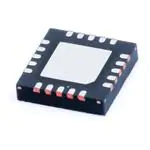
RGP PACKAGE
(TOP VIEW)
VDD2
•
•
Performs First Down-Conversion in 3.5-GHz
Radios (3300–3800 MHz)
Integrated LNA/Mixer/IF Amp/LO Buffer
Provision for External Image
Reject/Band-Pass Filter
Low Noise-Figure/High Linearity
Digital 10-dB Attenuator for High-Level
Signals
Frequency Range: 3.3–3.8 GHz
28 dB of Gain with 20 dB of Gain Control
(10-dB Fixed)
2.5-dB Noise Figure, Typical
LO Drive Level = 0 dBm, Typical
GND
•
P0031-02
DESCRIPTION
The TRF1216 is the first of two integrated circuits used in the receiver section of Texas Instruments’ 3.5-GHz
radio chipset. The TRF1216 down-converts the 3.5-GHz input frequency to an intermediate frequency in the
range of 400 MHz to 500 MHz. The device provides a differential output that passes through a SAW filter before
connecting to a second down converter. For the best performance, Texas Instruments TRF1212 should be used
to perform both the second down conversion and also provide the local oscillator for the TRF1216.
The TRF1216 includes a LNA with switchable attenuation, a balanced mixer, a variable gain IF amplifier and a
differential LO Buffer for improved performance. In order to provide exceptional image rejection and extra jammer
immunity, the TRF1216 offers a signal path to an off-chip filter. Specifications are provided assuming an in-band
2-dB insertion loss filter. To maximize input dynamic range, a 10-dB switchable attenuator is provided in the RF
path as well as 10 dB of analog IF gain control. After the image reject filter, an on-chip Balun converts the signal
from single ended to differential in order to provide better noise immunity at the mixer.
Please be aware that an important notice concerning availability, standard warranty, and use in critical applications of Texas
Instruments semiconductor products and disclaimers thereto appears at the end of this data sheet.
PRODUCTION DATA information is current as of publication date.
Products conform to specifications per the terms of the Texas
Instruments standard warranty. Production processing does not
necessarily include testing of all parameters.
Copyright © 2005, Texas Instruments Incorporated
�TRF1216
www.ti.com
SLWS172A – APRIL 2005 – REVISED DECEMBER 2005
These devices have limited built-in ESD protection. The leads should be shorted together or the device
placed in conductive foam during storage or handling to prevent electrostatic damage to the MOS gates.
BLOCK DIAGRAM
The detailed block diagram and the pin-out of the ASIC are shown in Figure 1 and Table 1.
VDD2
VDD1
VDDIF
LNAO MXRI
Dual Stage-LNA
VGA
Mixer
IFOP
IFON
BALUN
LNAI
IFB
RFAGC
LOP
LON
LO Buffer
GND
RFATTN
VDDLO
B0084-01
Figure 1. Detailed Block Diagram of TRF1216
TERMINAL FUNCTIONS
TERMINAL
NO.
NAME
I/O
TYPE
DESCRIPTION
1
LNAO
O
Analog
LNA Output, 50 Ω, ac-coupled
2
VDD1
I
Power
LNA1 DC Bias (+5 V nominal)
3, 4, 6, 9,
16, 19
GND
–
–
5
LNAI
I
Analog
RF input – Needs dc block and input matching for optimum noise figure
7
LOP
I
Analog
LO input positive, ac coupled
8
LON
I
Analog
LO input negative, ac coupled
10
VDDLO
I
Power
LO DC Bias (+5 V nominal)
11
IFB
–
–
12
VDDIF
I
Power
IF Bias Network dc Bias (+5 V nominal)
13
IFON
O
Analog
IF output and bias (see the application schematic for connections).
14
IFOP
O
Analog
IF output and bias (see the application schematic for connections).
15
RFAGC
I
Analog
Input voltage for analog gain control VRFAGC = 0 V to 1.5 V Max gain at VRFAGC = 0 V Min gain at
VRFAGC = 1.5 V
17
RFATTN
I
Digital
TTL control for switched attenuator TTL low – Attenuator switched in TTL high – Attenuator
switched out
Ground
Not connected for normal operation. IF Bias Adjustment. Do not ground this pin or connect to any
other pin.
18
MXRI
I
Analog
Mixer Input 50 Ω
20
VDD2
–
Power
LNA2 dc bias (+5 V nominal)
Back
GND
–
–
2
Back of package has metal base that must be grounded for thermal and RF performance.
�TRF1216
www.ti.com
SLWS172A – APRIL 2005 – REVISED DECEMBER 2005
ABSOLUTE MAXIMUM RATINGS
VALUES
UNIT
VDD
DC supply voltage, VDD
0 to 5.5
V
PIN
RF input power
10
dBm
TJ
Junction temperature
200
°C
PD
Power dissipation
1100
mW
VD
Digital input voltage
–0.3 to 5.5
V
VA
Analog input voltage
–0.3 to 5
V
θJC
Thermal resistance
9.1
°C/W
Tstg
Storage temperature
–40 to 105
°C
Top
Operating temperature
–40 to 85
°C
260
°C
junction-to-case (1)
Lead temperature (40 Sec Max)
(1)
Thermal resistance is junction to ambient assuming thermal pad with nine thermal vias under package metal base. See the
recommended PCB layout.
ELECTRICAL CHARACTERISTICS
The characteristics listed in the following tables are at VCC = 5 V, TA = 25°C unless otherwise specified.
PARAMETER
TEST CONDITIONS
MIN
TYP
MAX
UNIT
5
5.5
V
175
200
mA
DC CHARACTERISTICS
VDD
Supply voltage
IDD
Total supply current
I LNA1
LNA1 supply current
Pin 2 (VDD1)
35
mA
I LNA2
LNA2 supply current
Pin 20 (VDD2)
35
mA
IIF
IF AMP supply current
Pin 12 (VDDIF) plus IF drain bias on pins 13
and 14 (IFOP, IFON)
55
mA
ILO
LO supply current
Pin 10 (VDDLO)
50
mA
VAGC
Gain control voltage
0
2
V
IAGC
Gain control current
0
100
µA
VIH
Input high voltage
2.5
5
V
VIL
Input low voltage
0
0.8
V
IIH
Input high current
300
µA
IIL
Input low current
–50
µA
3
�TRF1216
www.ti.com
SLWS172A – APRIL 2005 – REVISED DECEMBER 2005
DOWNCONVERTER CHARACTERISTICS
Unless otherwise stated VDD = 5 V, FRF = 3500 MHz, TA = 25°C
MAX
UNIT
FRF
RF input frequency
PARAMETER
3300
3800
MHz
FLO
LO input frequency
2800
3400
MHz
FIF
IF output frequency
400
480
500
MHz
G
Maximum gain
VAGC = 0 V, RFATTN disabled, Measured into 100-Ω
differential load
27
30
33
dB
∆AGC
Analog gain control range
VAGC from 0 to 1.5 V, Any RFATTN setting. Measured
into 100-Ω differential load
7
10
∆ATTN
Switched attenuator range
RFATTN from high-to-low, any VAGC setting.
Measured into 100-Ω differential load
8.5
10
GHG
Gain flatness full band
Any 200-MHz band
GNB
Gain flatness / 6 MHz
Any 6-MHz band
Noise figure (1)
NF
IP-1dB
Input power at 1-dB compression
TEST CONDITIONS
MIN
TYP
1
VAGC = 0 V, RFATTN disabled
2.5
VAGC = 0 V, RFATTN enabled
4.8
VAGC = 1.5 V, RFATTN disabled
3.2
VAGC = 1.5 V, RFATTN enabled
6.8
VAGC = 0 V, RFATTN disabled
–17
VAGC = 0 V, RFATTN enabled
–6
VAGC = 1.5 V, RFATTN disabled
–10
VAGC = 1.5 V, RFATTN enabled
–4
VAGC = 0 V, RFATTN disabled
–7
VAGC = 0 V, RFATTN enabled
-1
VAGC = 1.5 V, RFATTN disabled
–5
VAGC = 1.5 V, RFATTN enabled
5
dB
11.5
dB
2
dB
0.4
dB
dB
dBm
IIP3
Input 3rd order intercept point
PLO
LO input power
Referenced to 100-Ω differential
LO to MXRI leakage
LO input = 3 dBm, VAGC = 0 V
–35
–45
dB
LO to IF leakage
LO input = 3 dBm, VAGC = 0 V
–40
–50
dB
LNAO to RXI isolation
FRF F = 3300 to 3800 MHz, RFATTN = TTL High
(1)
4
Assured by lab characterization/design and not subject to production test.
0
40
dBm
dBm
dB
�TRF1216
www.ti.com
SLWS172A – APRIL 2005 – REVISED DECEMBER 2005
TYPICAL CHARACTERISTICS
Measurements resulting in the following graphs were taken on the evaluation board of the ASIC (see Figure 9).
40
VAGC = 0 V
35
Gain With Attenuator Disabled
30
Gain − dB
25
20
15
Gain With Attenuator Enabled
10
5
0
3300
−40°C
25°C
85°C
3350
3400
3450
3500
3550
3600
3650
3700
3750
3800
f − Frequency − MHz
G001
Figure 2. Gain vs Frequency for VAGC = 0 V
30
−40°C
25°C
85°C
VAGC = 1.5 V
25
Gain − dB
20
Gain With Attenuator Disabled
15
10
Gain With Attenuator Enabled
5
0
3300
3350
3400
3450
3500
3550
3600
3650
3700
3750
3800
f − Frequency − MHz
G002
Figure 3. Gain vs Frequency for VAGC = 1.5 V
5
�TRF1216
www.ti.com
SLWS172A – APRIL 2005 – REVISED DECEMBER 2005
TYPICAL CHARACTERISTICS (continued)
30
TA = 25°C
25
Gain − dB
20
Attenuator Enabled
15
10
5
3300 MHz
3550 MHz
3800 MHz
0
0.00
0.25
Attenuator Disabled
0.50
0.75
1.00
1.25
1.50
VAGC − Analog Gain Control Voltage − V
G003
Figure 4. Gain vs VAGC for Different Frequencies, (TA = 25°C)
5
TA = 25°C
Input P1dB − dBm
0
−5
Attenuator Enabled, VAGC = 1.5 V
Attenuator Enabled, VAGC = 0 V
−10
Attenuator Disabled, VAGC = 1.5 V
−15
Attenuator Disabled, VAGC = 0 V
−20
−25
3300
3350
3400
3450
3500
3550
3600
3650
3700
3750
3800
f − Frequency − MHz
G004
Figure 5. Input P1dB vs Frequency, (TA = 25°C)
6
�TRF1216
www.ti.com
SLWS172A – APRIL 2005 – REVISED DECEMBER 2005
TYPICAL CHARACTERISTICS (continued)
10
TA = 25°C
Attenuator Enabled, VAGC = 1.5 V
0
Attenuator Enabled, VAGC = 0 V
Attenuator Disabled, VAGC = 1.5 V
−5
Attenuator Disabled, VAGC = 0 V
−10
−15
3300
3350
3400
3450
3500
3550
3600
3650
3700
3750
3800
f − Frequency − MHz
G005
Figure 6. Input IP3 vs Frequency, (TA = 25°C)
30
7
−40�C
25
6
25�C
20
5
85�C
15
4
85�C
10
25�C
5
NF [dB]
Gain [dB]
Input IP3 − dBm
5
3
2
−40�C
0
1
3.2
3.3
3.4
3.5
3.6
3.7
3.8
3.9
Frequency [GHz]
Figure 7. LNA Noise Figure vs Frequency With VAGC = 0 V
7
�TRF1216
www.ti.com
SLWS172A – APRIL 2005 – REVISED DECEMBER 2005
APPLICATION INFORMATION
A typical application schematic is shown in Figure 9.
The PCB material recommendations are shown in Table 1 and Figure 8.
Table 1. PCB Recommendations
Board Material
FR4
Board Material Core Thickness
10 mil
Copper Thickness (starting)
1 oz
Prepreg Thickness
8 mil
Recommended Number of Layers
4
Via Plating Thickness
1/2 oz
Final Plate
White immersion tin
Final Board Thickness
33–37 mil
Dia. 15 Mil
1 oz. Copper + ½ oz. Copper Plated
Upper and Lower Surfaces
Layer 1
10 Mil Core FR4
35 Mil
Layer 2: 1 oz. Copper
8 Mil
Prepreg
Layer 3: 1 oz. Copper
10 Mil Core FR4
DuPont CB 100
Conductive ViaPlug
Layer 4
½ oz. Copper Plated
M0020-02
NOTE: Top and bottom surface finish: copper flash with 50–70 µin white tin immersion.
Figure 8. PCB Construction and Via Cross Section
8
�TRF1216
www.ti.com
SLWS172A – APRIL 2005 – REVISED DECEMBER 2005
Z = 50 W
RFATTN
BPF
VDD
VRFAGC
(A)
100 pF
(A)
100 pF
0.01 mF
22 nH
(B)
IF OUT_POS
2
100 pF
16
3
4
10 pF
270 nH
GND
MXRI
RFATTN
17
LNAO
RFAGC
IFOP
VDD1
(A)
GND
IFON
GND
VDDIF
15
(A)
RF_IN
IFB
LNAI
7
LO_POS
GND
LON
LOP
GND
0W
6
8
9
0.01 mF
100 pF
270 nH
14
22 nH
13
(B)
IF OUT_NEG
12
VDD
(A)
5
VDD
11
100 pF
0.01 mF
VDDLO
0.01 mF
18
GND
Back
1
19
VDD2
20
10
(A)
100 pF
0.01 mF
LO_NEG
S0122-01
A.
Place 100-pF capacitors close to package pins.
B.
Place 22-nH inductors close to package pins.
Figure 9. Recommended Application Schematic
9
�TRF1216
www.ti.com
SLWS172A – APRIL 2005 – REVISED DECEMBER 2005
2.00
0.50 TYP
0.20 TYP
0.60 TYP
PIN 1
1.00 TYP
2.80
2.00
1.00 TYP
DIA 0.38 TYP
0.25 TYP
2.80
Solder Mask. No Solder Mask Under Chip, On Lead Pads or On Ground Connections.
Notes: 9 Via Holes, Each 0.38 mm.
Dimensions in mm
M0022-02
Figure 10. Recommended Pad Layout
10
�PACKAGE OPTION ADDENDUM
www.ti.com
9-Aug-2013
PACKAGING INFORMATION
Orderable Device
Status
(1)
Package Type Package Pins Package
Drawing
Qty
Eco Plan
Lead/Ball Finish
(2)
MSL Peak Temp
Op Temp (°C)
Device Marking
(3)
(4/5)
TRF1216IRGPR
ACTIVE
QFN
RGP
20
3000
Green (RoHS
& no Sb/Br)
CU SN
Level-3-260C-168 HR
-40 to 85
TRF
1216
TRF1216IRGPRG3
ACTIVE
QFN
RGP
20
3000
Green (RoHS
& no Sb/Br)
CU SN
Level-3-260C-168 HR
-40 to 85
TRF
1216
TRF1216IRGPT
ACTIVE
QFN
RGP
20
TBD
Call TI
Call TI
-40 to 85
TRF
1216
TRF1216IRGPTG3
ACTIVE
QFN
RGP
20
TBD
Call TI
Call TI
-40 to 85
TRF
1216
(1)
The marketing status values are defined as follows:
ACTIVE: Product device recommended for new designs.
LIFEBUY: TI has announced that the device will be discontinued, and a lifetime-buy period is in effect.
NRND: Not recommended for new designs. Device is in production to support existing customers, but TI does not recommend using this part in a new design.
PREVIEW: Device has been announced but is not in production. Samples may or may not be available.
OBSOLETE: TI has discontinued the production of the device.
(2)
Eco Plan - The planned eco-friendly classification: Pb-Free (RoHS), Pb-Free (RoHS Exempt), or Green (RoHS & no Sb/Br) - please check http://www.ti.com/productcontent for the latest availability
information and additional product content details.
TBD: The Pb-Free/Green conversion plan has not been defined.
Pb-Free (RoHS): TI's terms "Lead-Free" or "Pb-Free" mean semiconductor products that are compatible with the current RoHS requirements for all 6 substances, including the requirement that
lead not exceed 0.1% by weight in homogeneous materials. Where designed to be soldered at high temperatures, TI Pb-Free products are suitable for use in specified lead-free processes.
Pb-Free (RoHS Exempt): This component has a RoHS exemption for either 1) lead-based flip-chip solder bumps used between the die and package, or 2) lead-based die adhesive used between
the die and leadframe. The component is otherwise considered Pb-Free (RoHS compatible) as defined above.
Green (RoHS & no Sb/Br): TI defines "Green" to mean Pb-Free (RoHS compatible), and free of Bromine (Br) and Antimony (Sb) based flame retardants (Br or Sb do not exceed 0.1% by weight
in homogeneous material)
(3)
MSL, Peak Temp. -- The Moisture Sensitivity Level rating according to the JEDEC industry standard classifications, and peak solder temperature.
(4)
There may be additional marking, which relates to the logo, the lot trace code information, or the environmental category on the device.
(5)
Multiple Device Markings will be inside parentheses. Only one Device Marking contained in parentheses and separated by a "~" will appear on a device. If a line is indented then it is a continuation
of the previous line and the two combined represent the entire Device Marking for that device.
Important Information and Disclaimer:The information provided on this page represents TI's knowledge and belief as of the date that it is provided. TI bases its knowledge and belief on information
provided by third parties, and makes no representation or warranty as to the accuracy of such information. Efforts are underway to better integrate information from third parties. TI has taken and
Addendum-Page 1
Samples
�PACKAGE OPTION ADDENDUM
www.ti.com
9-Aug-2013
continues to take reasonable steps to provide representative and accurate information but may not have conducted destructive testing or chemical analysis on incoming materials and chemicals.
TI and TI suppliers consider certain information to be proprietary, and thus CAS numbers and other limited information may not be available for release.
In no event shall TI's liability arising out of such information exceed the total purchase price of the TI part(s) at issue in this document sold by TI to Customer on an annual basis.
Addendum-Page 2
�PACKAGE MATERIALS INFORMATION
www.ti.com
24-Apr-2013
TAPE AND REEL INFORMATION
*All dimensions are nominal
Device
Package Package Pins
Type Drawing
SPQ
Reel
Reel
A0
Diameter Width (mm)
(mm) W1 (mm)
B0
(mm)
K0
(mm)
P1
(mm)
W
Pin1
(mm) Quadrant
TRF1216IRGPR
QFN
RGP
20
3000
330.0
12.4
4.3
4.3
1.5
8.0
12.0
Q2
TRF1216IRGPT
QFN
RGP
20
250
180.0
12.4
4.3
4.3
1.5
8.0
12.0
Q2
Pack Materials-Page 1
�PACKAGE MATERIALS INFORMATION
www.ti.com
24-Apr-2013
*All dimensions are nominal
Device
Package Type
Package Drawing
Pins
SPQ
Length (mm)
Width (mm)
Height (mm)
TRF1216IRGPR
QFN
RGP
20
3000
338.1
338.1
20.6
TRF1216IRGPT
QFN
RGP
20
250
210.0
185.0
35.0
Pack Materials-Page 2
��IMPORTANT NOTICE
Texas Instruments Incorporated and its subsidiaries (TI) reserve the right to make corrections, enhancements, improvements and other
changes to its semiconductor products and services per JESD46, latest issue, and to discontinue any product or service per JESD48, latest
issue. Buyers should obtain the latest relevant information before placing orders and should verify that such information is current and
complete. All semiconductor products (also referred to herein as “components”) are sold subject to TI’s terms and conditions of sale
supplied at the time of order acknowledgment.
TI warrants performance of its components to the specifications applicable at the time of sale, in accordance with the warranty in TI’s terms
and conditions of sale of semiconductor products. Testing and other quality control techniques are used to the extent TI deems necessary
to support this warranty. Except where mandated by applicable law, testing of all parameters of each component is not necessarily
performed.
TI assumes no liability for applications assistance or the design of Buyers’ products. Buyers are responsible for their products and
applications using TI components. To minimize the risks associated with Buyers’ products and applications, Buyers should provide
adequate design and operating safeguards.
TI does not warrant or represent that any license, either express or implied, is granted under any patent right, copyright, mask work right, or
other intellectual property right relating to any combination, machine, or process in which TI components or services are used. Information
published by TI regarding third-party products or services does not constitute a license to use such products or services or a warranty or
endorsement thereof. Use of such information may require a license from a third party under the patents or other intellectual property of the
third party, or a license from TI under the patents or other intellectual property of TI.
Reproduction of significant portions of TI information in TI data books or data sheets is permissible only if reproduction is without alteration
and is accompanied by all associated warranties, conditions, limitations, and notices. TI is not responsible or liable for such altered
documentation. Information of third parties may be subject to additional restrictions.
Resale of TI components or services with statements different from or beyond the parameters stated by TI for that component or service
voids all express and any implied warranties for the associated TI component or service and is an unfair and deceptive business practice.
TI is not responsible or liable for any such statements.
Buyer acknowledges and agrees that it is solely responsible for compliance with all legal, regulatory and safety-related requirements
concerning its products, and any use of TI components in its applications, notwithstanding any applications-related information or support
that may be provided by TI. Buyer represents and agrees that it has all the necessary expertise to create and implement safeguards which
anticipate dangerous consequences of failures, monitor failures and their consequences, lessen the likelihood of failures that might cause
harm and take appropriate remedial actions. Buyer will fully indemnify TI and its representatives against any damages arising out of the use
of any TI components in safety-critical applications.
In some cases, TI components may be promoted specifically to facilitate safety-related applications. With such components, TI’s goal is to
help enable customers to design and create their own end-product solutions that meet applicable functional safety standards and
requirements. Nonetheless, such components are subject to these terms.
No TI components are authorized for use in FDA Class III (or similar life-critical medical equipment) unless authorized officers of the parties
have executed a special agreement specifically governing such use.
Only those TI components which TI has specifically designated as military grade or “enhanced plastic” are designed and intended for use in
military/aerospace applications or environments. Buyer acknowledges and agrees that any military or aerospace use of TI components
which have not been so designated is solely at the Buyer's risk, and that Buyer is solely responsible for compliance with all legal and
regulatory requirements in connection with such use.
TI has specifically designated certain components as meeting ISO/TS16949 requirements, mainly for automotive use. In any case of use of
non-designated products, TI will not be responsible for any failure to meet ISO/TS16949.
Products
Applications
Audio
www.ti.com/audio
Automotive and Transportation
www.ti.com/automotive
Amplifiers
amplifier.ti.com
Communications and Telecom
www.ti.com/communications
Data Converters
dataconverter.ti.com
Computers and Peripherals
www.ti.com/computers
DLP® Products
www.dlp.com
Consumer Electronics
www.ti.com/consumer-apps
DSP
dsp.ti.com
Energy and Lighting
www.ti.com/energy
Clocks and Timers
www.ti.com/clocks
Industrial
www.ti.com/industrial
Interface
interface.ti.com
Medical
www.ti.com/medical
Logic
logic.ti.com
Security
www.ti.com/security
Power Mgmt
power.ti.com
Space, Avionics and Defense
www.ti.com/space-avionics-defense
Microcontrollers
microcontroller.ti.com
Video and Imaging
www.ti.com/video
RFID
www.ti-rfid.com
OMAP Applications Processors
www.ti.com/omap
TI E2E Community
e2e.ti.com
Wireless Connectivity
www.ti.com/wirelessconnectivity
Mailing Address: Texas Instruments, Post Office Box 655303, Dallas, Texas 75265
Copyright © 2013, Texas Instruments Incorporated
�


 工商网监
湘ICP备2023018690号
工商网监
湘ICP备2023018690号
