SN74ALVCH16543
16-BIT REGISTERED TRANSCEIVER
WITH 3-STATE OUTPUTS
SCES025D – JULY 1995 – REVISED FEBRUARY 1999
D Member of the Texas Instruments
D
D
D
D
D
Widebus Family
EPIC (Enhanced-Performance Implanted
CMOS) Submicron Process
Bus Hold on Data Inputs Eliminates the
Need for External Pullup/Pulldown
Resistors
ESD Protection Exceeds 2000 V Per
MIL-STD-883, Method 3015; Exceeds 200 V
Using Machine Model (C = 200 pF, R = 0)
Latch-Up Performance Exceeds 250 mA Per
JESD 17
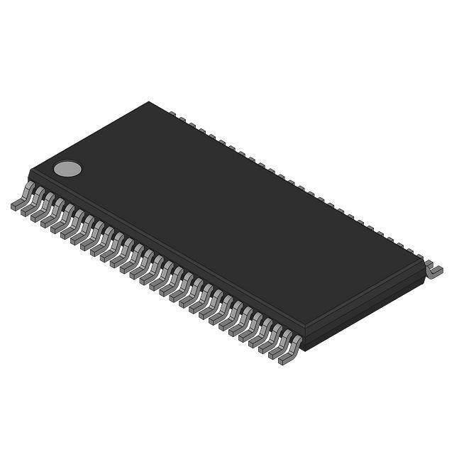
Package Options Include Plastic 300-mil
Shrink Small-Outline (DL) and Thin Shrink
Small-Outline (DGG) Packages
description
This 16-bit registered transceiver is designed for
1.65-V to 3.6-V VCC operation.
The SN74ALVCH16543 can be used as two 8-bit
transceivers or one 16-bit transceiver. Separate
latch-enable (LEAB or LEBA) and output-enable
(OEAB or OEBA) inputs are provided for each
register to permit independent control in either
direction of data flow.
The A-to-B enable (CEAB) input must be low to
enter data from A or to output data from B. If CEAB
is low and LEAB is low, the A-to-B latches are
transparent; a subsequent low-to-high transition
of LEAB puts the A latches in the storage mode.
With CEAB and OEAB both low, the 3-state
B outputs are active and reflect the data present
at the output of the A latches. Data flow from B to
A is similar, but requires using CEBA, LEBA, and
OEBA.
DGG OR DL PACKAGE
(TOP VIEW)
1OEAB
1LEAB
1CEAB
GND
1A1
1A2
VCC
1A3
1A4
1A5
GND
1A6
1A7
1A8
2A1
2A2
2A3
GND
2A4
2A5
2A6
VCC
2A7
2A8
GND
2CEAB
2LEAB
2OEAB
1
56
2
55
3
54
4
53
5
52
6
51
7
50
8
49
9
48
10
47
11
46
12
45
13
44
14
43
15
42
16
41
17
40
18
39
19
38
20
37
21
36
22
35
23
34
24
33
25
32
26
31
27
30
28
29
1OEBA
1LEBA
1CEBA
GND
1B1
1B2
VCC
1B3
1B4
1B5
GND
1B6
1B7
1B8
2B1
2B2
2B3
GND
2B4
2B5
2B6
VCC
2B7
2B8
GND
2CEBA
2LEBA
2OEBA
To ensure the high-impedance state during power up or power down, OE should be tied to VCC through a pullup
resistor; the minimum value of the resistor is determined by the current-sinking capability of the driver.
Active bus-hold circuitry is provided to hold unused or floating data inputs at a valid logic level.
The SN74ALVCH16543 is characterized for operation from –40°C to 85°C.
EPIC and Widebus are trademarks of Texas Instruments Incorporated.
Copyright 1999, Texas Instruments Incorporated
PRODUCTION DATA information is current as of publication date.
Products conform to specifications per the terms of Texas Instruments
standard warranty. Production processing does not necessarily include
testing of all parameters.
POST OFFICE BOX 655303
• DALLAS, TEXAS 75265
3–213
�SN74ALVCH16543
16-BIT REGISTERED TRANSCEIVER
WITH 3-STATE OUTPUTS
SCES025D – JULY 1995 – REVISED FEBRUARY 1999
logic symbol†
1OEBA
1CEBA
1LEBA
1OEAB
1CEAB
1LEAB
2OEBA
2CEBA
2LEBA
2OEAB
2CEAB
56
54
55
1
G1
1C5
2EN4
3
G2
2
2C6
29
31
30
28
26
27
2LEAB
1A1
1EN3
7EN9
G7
7C11
8EN10
G8
8C12
5
3
6D
1A2
1A3
1A4
1A5
1A6
1A7
1A8
2A1
6
2A3
2A4
2A5
2A6
2A7
2A8
4
51
49
9
48
10
47
12
45
13
44
14
43
15
9
16
11D
10
42
41
17
40
19
38
20
37
21
36
23
34
24
33
† This symbol is in accordance with ANSI/IEEE Std 91-1984 and IEC Publication 617-12.
3–214
52
8
12D
2A2
5D
POST OFFICE BOX 655303
• DALLAS, TEXAS 75265
1B1
1B2
1B3
1B4
1B5
1B6
1B7
1B8
2B1
2B2
2B3
2B4
2B5
2B6
2B7
2B8
�SN74ALVCH16543
16-BIT REGISTERED TRANSCEIVER
WITH 3-STATE OUTPUTS
SCES025D – JULY 1995 – REVISED FEBRUARY 1999
logic diagram (positive logic)
1OEBA
1CEBA
1LEBA
1OEAB
1CEAB
1LEAB
1A1
56
54
55
1
3
2
C1
5
1D
52
1B1
C1
1D
To Seven Other Channels
2OEBA
2CEBA
2LEBA
2OEAB
2CEAB
2LEAB
2A1
29
31
30
28
26
27
C1
15
1D
42
2B1
C1
1D
To Seven Other Channels
POST OFFICE BOX 655303
• DALLAS, TEXAS 75265
3–215
�SN74ALVCH16543
16-BIT REGISTERED TRANSCEIVER
WITH 3-STATE OUTPUTS
SCES025D – JULY 1995 – REVISED FEBRUARY 1999
FUNCTION TABLE†
(each 8-bit section)
INPUTS
CEAB
LEAB
OEAB
A
OUTPUT
B
H
X
X
X
Z
X
X
H
X
Z
L
H
L
X
L
L
L
L
B0‡
L
L
L
L
H
H
† A-to-B data flow is shown; B-to-A flow control is the
same except that it uses CEBA, LEBA, and OEBA.
‡ Output level before the indicated steady-state input
conditions were established
absolute maximum ratings over operating free-air temperature range (unless otherwise noted)§
Supply voltage range, VCC . . . . . . . . . . . . . . . . . . . . . . . . . . . . . . . . . . . . . . . . . . . . . . . . . . . . . . . . . –0.5 V to 4.6 V
Input voltage range, VI: Except I/O ports (see Note 1) . . . . . . . . . . . . . . . . . . . . . . . . . . . . . . . . . –0.5 V to 4.6 V
I/O ports (see Notes 1 and 2) . . . . . . . . . . . . . . . . . . . . . . . . . . . –0.5 V to VCC + 0.5 V
Output voltage range, VO (see Notes 1 and 2) . . . . . . . . . . . . . . . . . . . . . . . . . . . . . . . . . . –0.5 V to VCC + 0.5 V
Input clamp current, IIK (VI < 0) . . . . . . . . . . . . . . . . . . . . . . . . . . . . . . . . . . . . . . . . . . . . . . . . . . . . . . . . . . . –50 mA
Output clamp current, IOK (VO < 0) . . . . . . . . . . . . . . . . . . . . . . . . . . . . . . . . . . . . . . . . . . . . . . . . . . . . . . . . –50 mA
Continuous output current, IO . . . . . . . . . . . . . . . . . . . . . . . . . . . . . . . . . . . . . . . . . . . . . . . . . . . . . . . . . . . . . ±50 mA
Continuous current through each VCC or GND . . . . . . . . . . . . . . . . . . . . . . . . . . . . . . . . . . . . . . . . . . . . . ±100 mA
Package thermal impedance, θJA (see Note 3): DGG package . . . . . . . . . . . . . . . . . . . . . . . . . . . . . . . . 81°C/W
DL package . . . . . . . . . . . . . . . . . . . . . . . . . . . . . . . . . . 74°C/W
Storage temperature range, Tstg . . . . . . . . . . . . . . . . . . . . . . . . . . . . . . . . . . . . . . . . . . . . . . . . . . . . 65°C to 150°C
§ Stresses beyond those listed under “absolute maximum ratings” may cause permanent damage to the device. These are stress ratings only, and
functional operation of the device at these or any other conditions beyond those indicated under “recommended operating conditions” is not
implied. Exposure to absolute-maximum-rated conditions for extended periods may affect device reliability.
NOTES: 1. The input negative-voltage and output voltage ratings may be exceeded if the input and output current ratings are observed.
2. This value is limited to 4.6 V maximum.
3. The package thermal impedance is calculated in accordance with JESD 51.
3–216
POST OFFICE BOX 655303
• DALLAS, TEXAS 75265
�SN74ALVCH16543
16-BIT REGISTERED TRANSCEIVER
WITH 3-STATE OUTPUTS
SCES025D – JULY 1995 – REVISED FEBRUARY 1999
recommended operating conditions (see Note 4)
VCC
VIH
Supply voltage
VCC = 1.65 V to 1.95 V
VCC = 2.3 V to 2.7 V
High-level input voltage
VCC = 2.7 V to 3.6 V
VCC = 1.65 V to 1.95 V
VIL
Low-level input voltage
VI
VO
Input voltage
IOH
IOL
∆t/∆v
MIN
MAX
1.65
3.6
2
0.35 × VCC
0.7
VCC = 2.7 V
VCC = 3 V
VCC = 1.65 V
VCC = 2.3 V
Low-level output current
VCC = 2.7 V
VCC = 3 V
Input transition rise or fall rate
V
0.8
0
High-level output current
V
1.7
0
VCC = 1.65 V
VCC = 2.3 V
V
0.65 × VCC
VCC = 2.3 V to 2.7 V
VCC = 2.7 V to 3.6 V
Output voltage
UNIT
VCC
VCC
V
V
–4
–12
–12
mA
–24
4
12
12
mA
24
10
ns/V
TA
Operating free-air temperature
–40
85
°C
NOTE 4: All unused control inputs of the device must be held at VCC or GND to ensure proper device operation. Refer to the TI application report,
Implications of Slow or Floating CMOS Inputs, literature number SCBA004.
POST OFFICE BOX 655303
• DALLAS, TEXAS 75265
3–217
�SN74ALVCH16543
16-BIT REGISTERED TRANSCEIVER
WITH 3-STATE OUTPUTS
SCES025D – JULY 1995 – REVISED FEBRUARY 1999
electrical characteristics over recommended operating free-air temperature range (unless
otherwise noted)
PARAMETER
TEST CONDITIONS
VCC
1.65 V to 3.6 V
IOH = –100 µA
IOH = –4 mA
1.65 V
IOH = –6 mA
VOH
IOH = –12 mA
IOH = –24 mA
IOL = 100 µA
UNIT
VCC–0.2
1.2
2.3 V
2
2.3 V
1.7
2.7 V
2.2
3V
2.4
3V
2
V
0.2
0.45
2.3 V
0.4
2.3 V
0.7
2.7 V
0.4
3V
0.55
3.6 V
±5
IOL = 24 mA
VI = VCC or GND
II(hold)
MAX
1.65 V
IOL = 12 mA
II
TYP†
1.65 V to 3.6 V
IOL = 4 mA
IOL = 6 mA
VOL
MIN
VI = 0.58 V
VI = 1.07 V
1.65 V
25
1.65 V
–25
VI = 0.7 V
VI = 1.7 V
2.3 V
45
2.3 V
–45
VI = 0.8 V
VI = 2 V
3V
75
3V
–75
V
µA
µA
VI = 0 to 3.6 V‡
3.6 V
±500
IOZ§
ICC
VO = VCC or GND
VI = VCC or GND,
3.6 V
±10
µA
40
µA
∆ICC
Ci
One input at VCC – 0.6 V,
750
µA
Control inputs
IO = 0
Other inputs at VCC or GND
VI = VCC or GND
VO = VCC or GND
3.6 V
3 V to 3.6 V
3.3 V
3.5
pF
Cio
A or B ports
3.3 V
8.5
pF
† All typical values are at VCC = 3.3 V, TA = 25°C.
‡ This is the bus-hold maximum dynamic current. It is the minimum overdrive current required to switch the input from one state to another.
§ For I/O ports, the parameter IOZ includes the input leakage current.
timing requirements over recommended operating free-air temperature range (unless otherwise
noted) (see Figures 1 through 3)
VCC = 1.8 V
tw
tsu
MIN
¶
Pulse duration, LE or CE low
MAX
VCC = 2.5 V
± 0.2 V
MIN
MAX
VCC = 2.7 V
MIN
MAX
VCC = 3.3 V
± 0.3 V
MIN
UNIT
MAX
3.3
3.3
3.3
ns
¶
1.2
1.5
1.2
ns
th
Hold time
Data after LE↑ or CE↑
¶ This information was not available at the time of publication.
¶
1.2
0.8
1.3
ns
3–218
• DALLAS, TEXAS 75265
Setup time
Data before LE↑ or CE↑
POST OFFICE BOX 655303
�SN74ALVCH16543
16-BIT REGISTERED TRANSCEIVER
WITH 3-STATE OUTPUTS
SCES025D – JULY 1995 – REVISED FEBRUARY 1999
switching characteristics over recommended operating free-air temperature range (unless
otherwise noted) (see Figures 1 through 3)
PARAMETER
FROM
(INPUT)
TO
(OUTPUT)
A or B
tpd
ten
tdis
ten
tdis
VCC = 1.8 V
VCC = 2.5 V
± 0.2 V
MIN
MAX
B or A
TYP
†
1
LE
A or B
†
CE
A or B
CE
A or B
OE
OE
VCC = 2.7 V
MIN
VCC = 3.3 V
± 0.3 V
UNIT
MAX
MIN
MAX
5.1
4.8
1
4.3
1
6.5
6.2
1.1
5
†
1
7.2
6.9
1
5.6
ns
†
1.3
6.1
6.2
1.5
5.1
ns
A or B
†
1
6.8
6.3
1
5.3
ns
A or B
†
1
5.7
4.8
1.1
4.6
ns
ns
† This information was not available at the time of publication.
operating characteristics, TA = 25°C
PARAMETER
Cpd
Power dissipation
capacitance
TEST CONDITIONS
Outputs enabled
Outputs disabled
CL = 50 pF,
VCC = 1.8 V
TYP
†
f = 10 MHz
†
VCC = 2.5 V
TYP
VCC = 3.3 V
TYP
54
64
6
7
UNIT
pF
† This information was not available at the time of publication.
POST OFFICE BOX 655303
• DALLAS, TEXAS 75265
3–219
�SN74ALVCH16543
16-BIT REGISTERED TRANSCEIVER
WITH 3-STATE OUTPUTS
SCES025D – JULY 1995 – REVISED FEBRUARY 1999
PARAMETER MEASUREMENT INFORMATION
VCC = 1.8 V
2 × VCC
S1
1 kΩ
From Output
Under Test
Open
GND
CL = 30 pF
(see Note A)
1 kΩ
TEST
S1
tpd
tPLZ/tPZL
tPHZ/tPZH
Open
2 × VCC
GND
LOAD CIRCUIT
tw
VCC
Timing
Input
VCC/2
VCC/2
VCC/2
0V
VOLTAGE WAVEFORMS
SETUP AND HOLD TIMES
VCC/2
Output
Control
(low-level
enabling)
VCC
VCC/2
VCC/2
0V
tPLH
Output
Waveform 1
S1 at 2 × VCC
(see Note B)
VOH
VCC/2
tPLZ
VCC
VCC/2
tPZH
tPHL
VCC/2
VOL
VCC/2
0V
tPZL
VCC
Input
VOLTAGE WAVEFORMS
PULSE DURATION
th
VCC
Data
Input
VCC/2
0V
0V
tsu
Output
VCC
VCC/2
Input
Output
Waveform 2
S1 at GND
(see Note B)
VOL + 0.15 V
VOL
tPHZ
VCC/2
VOH
VOH – 0.15 V
0V
VOLTAGE WAVEFORMS
ENABLE AND DISABLE TIMES
VOLTAGE WAVEFORMS
PROPAGATION DELAY TIMES
NOTES: A. CL includes probe and jig capacitance.
B. Waveform 1 is for an output with internal conditions such that the output is low except when disabled by the output control.
Waveform 2 is for an output with internal conditions such that the output is high except when disabled by the output control.
C. All input pulses are supplied by generators having the following characteristics: PRR ≤ 10 MHz, ZO = 50 Ω, tr ≤ 2 ns, tf ≤ 2 ns.
D. The outputs are measured one at a time with one transition per measurement.
E. tPLZ and tPHZ are the same as tdis.
F. tPZL and tPZH are the same as ten.
G. tPLH and tPHL are the same as tpd.
Figure 1. Load Circuit and Voltage Waveforms
3–220
POST OFFICE BOX 655303
• DALLAS, TEXAS 75265
�SN74ALVCH16543
16-BIT REGISTERED TRANSCEIVER
WITH 3-STATE OUTPUTS
SCES025D – JULY 1995 – REVISED FEBRUARY 1999
PARAMETER MEASUREMENT INFORMATION
VCC = 2.5 V ± 0.2 V
2 × VCC
S1
500 Ω
From Output
Under Test
Open
GND
CL = 30 pF
(see Note A)
500 Ω
TEST
S1
tpd
tPLZ/tPZL
tPHZ/tPZH
Open
2 × VCC
GND
LOAD CIRCUIT
tw
VCC
Timing
Input
VCC/2
VCC/2
VCC/2
0V
VOLTAGE WAVEFORMS
SETUP AND HOLD TIMES
VCC/2
VCC/2
0V
tPLH
Output
Control
(low-level
enabling)
tPLZ
VCC
VCC/2
tPZH
VOH
VCC/2
VOL
VCC/2
0V
Output
Waveform 1
S1 at 2 × VCC
(see Note B)
tPHL
VCC/2
VCC
VCC/2
tPZL
VCC
Input
VOLTAGE WAVEFORMS
PULSE DURATION
th
VCC
Data
Input
VCC/2
0V
0V
tsu
Output
VCC
VCC/2
Input
Output
Waveform 2
S1 at GND
(see Note B)
VOL + 0.15 V
VOL
tPHZ
VCC/2
VOH
VOH – 0.15 V
0V
VOLTAGE WAVEFORMS
ENABLE AND DISABLE TIMES
VOLTAGE WAVEFORMS
PROPAGATION DELAY TIMES
NOTES: A. CL includes probe and jig capacitance.
B. Waveform 1 is for an output with internal conditions such that the output is low except when disabled by the output control.
Waveform 2 is for an output with internal conditions such that the output is high except when disabled by the output control.
C. All input pulses are supplied by generators having the following characteristics: PRR ≤ 10 MHz, ZO = 50 Ω, tr ≤ 2 ns, tf ≤ 2 ns.
D. The outputs are measured one at a time with one transition per measurement.
E. tPLZ and tPHZ are the same as tdis.
F. tPZL and tPZH are the same as ten.
G. tPLH and tPHL are the same as tpd.
Figure 2. Load Circuit and Voltage Waveforms
POST OFFICE BOX 655303
• DALLAS, TEXAS 75265
3–221
�SN74ALVCH16543
16-BIT REGISTERED TRANSCEIVER
WITH 3-STATE OUTPUTS
SCES025D – JULY 1995 – REVISED FEBRUARY 1999
PARAMETER MEASUREMENT INFORMATION
VCC = 2.7 V AND 3.3 V ± 0.3 V
6V
S1
500 Ω
From Output
Under Test
Open
GND
CL = 50 pF
(see Note A)
500 Ω
TEST
S1
tpd
tPLZ/tPZL
tPHZ/tPZH
Open
6V
GND
tw
LOAD CIRCUIT
2.7 V
2.7 V
Timing
Input
Input
1.5 V
1.5 V
0V
1.5 V
0V
tsu
VOLTAGE WAVEFORMS
PULSE DURATION
th
2.7 V
Data
Input
1.5 V
1.5 V
0V
VOLTAGE WAVEFORMS
SETUP AND HOLD TIMES
Output
Control
(low-level
enabling)
2.7 V
1.5 V
0V
tPZL
2.7 V
Input
1.5 V
1.5 V
0V
tPLH
VOH
Output
1.5 V
Output
Waveform 1
S1 at 6 V
(see Note B)
tPLZ
3V
1.5 V
tPZH
tPHL
1.5 V
VOL
1.5 V
Output
Waveform 2
S1 at GND
(see Note B)
VOL + 0.3 V
VOL
tPHZ
1.5 V
VOH
VOH – 0.3 V
0V
VOLTAGE WAVEFORMS
ENABLE AND DISABLE TIMES
VOLTAGE WAVEFORMS
PROPAGATION DELAY TIMES
NOTES: A. CL includes probe and jig capacitance.
B. Waveform 1 is for an output with internal conditions such that the output is low except when disabled by the output control.
Waveform 2 is for an output with internal conditions such that the output is high except when disabled by the output control.
C. All input pulses are supplied by generators having the following characteristics: PRR ≤ 10 MHz, ZO = 50 Ω, tr ≤ 2.5 ns, tf ≤ 2.5 ns.
D. The outputs are measured one at a time with one transition per measurement.
E. tPLZ and tPHZ are the same as tdis.
F. tPZL and tPZH are the same as ten.
G. tPLH and tPHL are the same as tpd.
Figure 3. Load Circuit and Voltage Waveforms
3–222
POST OFFICE BOX 655303
• DALLAS, TEXAS 75265
�


 工商网监
湘ICP备2023018690号
工商网监
湘ICP备2023018690号
