Sample &
Buy
Product
Folder
Support &
Community
Tools &
Software
Technical
Documents
SN54HC245, SN74HC245
SCLS131E – DECEMBER 1982 – REVISED SEPTEMBER 2015
SNx4HC245 Octal Bus Transceivers With 3-State Outputs
1 Features
3 Description
•
•
These octal bus transceivers are designed for
asynchronous two-way communication between data
buses. The control-function implementation minimizes
external timing requirements.
1
•
•
•
•
•
Wide Operating Voltage Range of 2 V to 6 V
High-Current 3-State Outputs Drive Bus Lines
Directly or Up to 15 LSTTL Loads
Low Power Consumption, 80-μA Max ICC
Typical tpd = 12 ns
±6-mA Output Drive at 5 V
Low Input Current of 1 μA Max
On Products Compliant to MIL-PRF-38535,
All Parameters Are Tested Unless Otherwise
Noted. On All Other Products, Production
Processing Does Not Necessarily Include Testing
of All Parameters.
2 Applications
•
•
•
•
•
•
Servers
PCs and Notebooks
Network Switches
Wearable Health and Fitness Devices
Telecom Infrastructures
Electronic Points of Sale
The devices allow data transmission from the A bus
to the B bus or from the B bus to the A bus,
depending on the logic level at the direction-control
(DIR) input. The output-enable (OE) input can be
used to disable the device so that the buses are
effectively isolated.
Device Information
PART NUMBER
SNx4HC245
PACKAGE
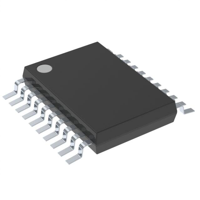
BODY SIZE (NOM)
SSOP (20)
7.20 mm × 5.30 mm
SOIC (20)
12.80 mm × 7.50 mm
PDIP (20)
24.33 mm × 6.35 mm
SOP (20)
12.60 mm × 5.30 mm
TSSOP (20)
6.50 mm × 4.40 mm
(1) For all available packages, see the orderable addendum at
the end of the data sheet.
Logic Diagram (Positive Logic)
DIR
1
19
A1
OE
2
18
B1
To Seven Other Channels
1
An IMPORTANT NOTICE at the end of this data sheet addresses availability, warranty, changes, use in safety-critical applications,
intellectual property matters and other important disclaimers. PRODUCTION DATA.
�SN54HC245, SN74HC245
SCLS131E – DECEMBER 1982 – REVISED SEPTEMBER 2015
www.ti.com
Table of Contents
1
2
3
4
5
6
7
8
Features ..................................................................
Applications ...........................................................
Description .............................................................
Revision History.....................................................
Pin Configuration and Functions .........................
Specifications.........................................................
1
1
1
2
3
4
6.1
6.2
6.3
6.4
6.5
6.6
6.7
6.8
6.9
4
4
4
5
5
5
6
6
6
Absolute Maximum Ratings ......................................
ESD Ratings..............................................................
Recommended Operating Conditions.......................
Thermal Information ..................................................
Electrical Characteristics...........................................
Switching Characteristics, CL = 50 pF ......................
Switching Characteristics, CL = 150 pF ....................
Operating Characteristics..........................................
Typical Characteristics ..............................................
Parameter Measurement Information .................. 7
Detailed Description .............................................. 8
8.1 Overview ................................................................... 8
8.2 Functional Block Diagram ......................................... 8
8.3 Feature Description................................................... 8
8.4 Device Functional Modes.......................................... 8
9
Application and Implementation .......................... 9
9.1 Application Information.............................................. 9
9.2 Typical Application ................................................... 9
10 Power Supply Recommendations ..................... 10
11 Layout................................................................... 10
11.1 Layout Guidelines ................................................. 10
11.2 Layout Example .................................................... 10
12 Device and Documentation Support ................. 11
12.1
12.2
12.3
12.4
12.5
Related Links ........................................................
Community Resources..........................................
Trademarks ...........................................................
Electrostatic Discharge Caution ............................
Glossary ................................................................
11
11
11
11
11
13 Mechanical, Packaging, and Orderable
Information ........................................................... 11
4 Revision History
NOTE: Page numbers for previous revisions may differ from page numbers in the current version.
Changes from Revision D (August 2003) to Revision E
Page
•
Added Device Comparison section, Thermal Informationsection , ESD Ratings section, Application and
Implementation section, Power Supply Recommendations section, and Layout section. ..................................................... 1
•
Added Military Disclaimer to Features list. ............................................................................................................................. 1
•
Updated FK package pinout drawing. .................................................................................................................................... 3
2
Submit Documentation Feedback
Copyright © 1982–2015, Texas Instruments Incorporated
Product Folder Links: SN54HC245 SN74HC245
�SN54HC245, SN74HC245
www.ti.com
SCLS131E – DECEMBER 1982 – REVISED SEPTEMBER 2015
5 Pin Configuration and Functions
1
20
2
19
3
18
4
17
5
16
6
15
7
14
8
13
9
12
10
11
VCC
OE
B1
B2
B3
B4
B5
B6
B7
B8
A2
A1
DIR
VCC
A3
A4
A5
A6
A7
4
3 2 1 20 19
18
5
17
6
16
7
15
8
14
9 10 11 12 13
B1
B2
B3
B4
B5
A8
GND
B8
B7
B6
DIR
A1
A2
A3
A4
A5
A6
A7
A8
GND
OE
FK Package
20-Pin LCCC
Top View
DB, DGV, DW, N, J, W, or PW Package
20-Pin SSOP, TVSOP, SOIC, PDIP CDIP, CFP, or TSSOP
Top View
Pin Functions
PIN
NO.
NAME
I/O
DESCRIPTION
1
DIR
I/O
Direction Pin
2
A1
I/O
A1 Input/Output
3
A2
I/O
A2 Input/Output
4
A3
I/O
A3 Input/Output
5
A4
I/O
A4 Input/Output
6
A5
I/O
A5 Input/Output
7
A6
I/O
A6 Input/Output
8
A7
I/O
A7 Input/Output
9
A8
I/O
A8 Input/Output
10
GND
—
Ground Pin
11
B8
I/O
B8 Input/Output
12
B7
I/O
B7 Input/Output
13
B6
I/O
B6 Input/Output
14
B5
I/O
B5 Input/Output
15
B4
I/O
B4 Input/Output
16
B3
I/O
B3 Input/Output
17
B2
I/O
B2 Input/Output
18
B1
I/O
B1 Input/Output
19
OE
I/O
Output Enable
20
VCC
—
Power Pin
Copyright © 1982–2015, Texas Instruments Incorporated
Product Folder Links: SN54HC245 SN74HC245
Submit Documentation Feedback
3
�SN54HC245, SN74HC245
SCLS131E – DECEMBER 1982 – REVISED SEPTEMBER 2015
www.ti.com
6 Specifications
6.1 Absolute Maximum Ratings
over operating free-air temperature range (unless otherwise noted) (1)
VCC
Supply voltage
(2)
MIN
MAX
UNIT
−0.5
7
V
IIK
Input clamp current
VI < 0 or VI > VCC
±20
mA
IOK
Output clamp current (2)
VO < 0 or VO > VCC
±20
mA
IO
Continuous output current
VO = 0 to VCC
±35
mA
±70
mA
150
°C
Continuous current through VCC or GND
Tstg
(1)
(2)
Storage temperature
–65
Stresses beyond those listed under Absolute Maximum Ratings may cause permanent damage to the device. These are stress ratings
only, and functional operation of the device at these or any other conditions beyond those indicated under Recommended Operating
Conditions is not implied. Exposure to absolute-maximum-rated conditions for extended periods may affect device reliability.
The input and output voltage ratings may be exceeded if the input and output current ratings are observed.
6.2 ESD Ratings
VALUE
V(ESD)
(1)
(2)
Electrostatic discharge
Human body model (HBM), per ANSI/ESDA/JEDEC JS-001 (1)
±3000
Charged-device model (CDM), per JEDEC specification JESD22C101 (2)
±1000
UNIT
V
JEDEC document JEP155 states that 500-V HBM allows safe manufacturing with a standard ESD control process.
JEDEC document JEP157 states that 250-V CDM allows safe manufacturing with a standard ESD control process.
6.3 Recommended Operating Conditions
over operating free-air temperature range (unless otherwise noted) (1)
SN54HC245
VCC
Supply voltage
VIH
High-level input voltage
VCC = 2 V
VCC = 4.5 V
VCC = 6 V
NOM
MAX
MIN
NOM
MAX
2
5
6
2
5
6
1.5
1.5
3.15
3.15
4.2
4.2
VCC = 2 V
VIL
Low-level input voltage
SN74HC245
MIN
VCC = 4.5 V
VCC = 6 V
UNIT
V
V
0.5
0.5
1.35
1.35
1.8
1.8
V
VI
Input voltage
0
VCC
0
VCC
V
VO
Output voltage
0
VCC
0
VCC
V
VCC = 2 V
∆t/∆v
Input transition rise and fall time
TA
Operating free-air temperature
VCC = 4.5 V
VCC = 6 V
(1)
4
1000
1000
500
500
400
–55
125
ns
400
–40
85
°C
All unused inputs of the device must be held at VCC or GND to ensure proper device operation. Refer to the TI application report,
Implications of Slow or Floating CMOS Inputs, literature number SCBA004.
Submit Documentation Feedback
Copyright © 1982–2015, Texas Instruments Incorporated
Product Folder Links: SN54HC245 SN74HC245
�SN54HC245, SN74HC245
www.ti.com
SCLS131E – DECEMBER 1982 – REVISED SEPTEMBER 2015
6.4 Thermal Information
SNx4HC245
THERMAL METRIC
DB
(SSOP)
(1)
DW
(SOIC)
N
(PDIP)
NS
(SOP)
PW
(TSSOP)
UNIT
20 PINS
RθJA
Junction-to-ambient thermal resistance
92.1
77.0
57.0
74.1
99.7
°C/W
RθJC(top)
Junction-to-case (top) thermal resistance
53.9
41.5
48.6
40.6
34.0
°C/W
RθJB
Junction-to-board thermal resistance
47.2
44.8
38.0
41.6
50.7
°C/W
ψJT
Junction-to-top characterization parameter
16.5
16.8
25.4
14.8
1.8
°C/W
ψJB
Junction-to-board characterization parameter
46.8
44.3
37.8
41.2
50.1
°C/W
(1)
For more information about traditional and new thermal metrics, see the Semiconductor and IC Package Thermal Metrics application
report, SPRA953.
6.5 Electrical Characteristics
over recommended operating free-air temperature range (unless otherwise noted)
PARAMETER
TEST CONDITIONS
VCC
IOH = –20 µA
VOH
VI = VIH or VIL
IOH = –6 mA
IOH = –7.8 mA
VOL
TA = 25°C
MIN
TYP
MAX
SN54HC245
SN74HC245
MIN
MIN
MAX
2V
1.9
1.998
1.9
1.9
4.5 V
4.4
4.499
4.4
4.4
6V
5.9
5.999
5.9
5.9
4.5 V
3.98
4.3
3.7
3.84
6V
5.48
5.8
5.2
V
5.34
2V
0.002
0.1
0.1
0.1
IOL = 20 µA
4.5 V
0.001
0.1
0.1
0.1
6V
0.001
0.1
0.1
0.1
IOL = 6 mA
4.5 V
0.17
0.26
0.4
0.33
6V
0.15
0.26
0.4
0.33
VI = VIH or VIL
IOL = 7.8 mA
UNIT
MAX
V
II
DIR or OE VI = VCC or 0
6V
±0.1
±100
±1000
±1000
nA
IOZ
A or B
6V
±0.01
±0.5
±10
±5
µA
8
160
80
µA
3
10
10
10
pF
ICC
Ci
VO = VCC or 0
VI = VCC or 0,
IO = 0
6V
DIR or OE
2 V to 6 V
6.6 Switching Characteristics, CL = 50 pF
over recommended operating free-air temperature range (unless otherwise noted)
(see Figure 3)
PARAMETER
tpd
ten
tdis
tt
FROM
(INPUT)
A or B
OE
OE
TO
(OUTPUT)
B or A
A or B
A or B
A or B
VCC
TA = 25°C
MIN
SN54HC245
MIN
SN74HC245
TYP
MAX
MAX
MIN
MAX
2V
40
105
160
130
4.5 V
15
21
32
26
6V
12
18
27
22
2V
125
230
340
290
4.5 V
23
46
68
58
6V
20
39
58
49
2V
74
200
300
250
4.5 V
25
40
60
50
6V
21
34
51
43
2V
20
60
90
75
4.5 V
8
12
18
15
6V
6
10
15
13
Copyright © 1982–2015, Texas Instruments Incorporated
Product Folder Links: SN54HC245 SN74HC245
UNIT
Submit Documentation Feedback
ns
ns
ns
ns
5
�SN54HC245, SN74HC245
SCLS131E – DECEMBER 1982 – REVISED SEPTEMBER 2015
www.ti.com
6.7 Switching Characteristics, CL = 150 pF
over recommended operating free-air temperature range (unless otherwise noted)
(see Figure 3)
PARAMETER
FROM
(INPUT)
TO
(OUTPUT)
VCC
tpd
A or B
B or A
ten
OE
A or B
tt
A or B
TA = 25°C
MIN
SN54HC245
SN74HC245
MIN
MIN
TYP
MAX
MAX
2V
54
135
200
170
4.5 V
18
27
40
34
6V
15
23
34
29
2V
150
270
405
335
4.5 V
31
54
81
67
6V
25
46
69
56
2V
45
210
315
265
4.5 V
17
42
63
53
6V
13
36
53
45
UNIT
MAX
ns
ns
ns
6.8 Operating Characteristics
TA = 25°C
PARAMETER
Cpd
TEST CONDITIONS
Power dissipation capacitance per transceiver
TYP
No load
UNIT
40
pF
45
45
40
40
35
35
30
30
25
25
TPD
TPD
6.9 Typical Characteristics
20
15
10
10
5
5
0
0
0
1
2
3
4
5
VCC at 25C
Submit Documentation Feedback
6
7
0
1
2
3
4
5
VCC at 25C
C002
Figure 1. TPD vs VCC at 25°C
6
20
15
6
7
C002
Figure 2. TPD vs VCC at 25°C
Copyright © 1982–2015, Texas Instruments Incorporated
Product Folder Links: SN54HC245 SN74HC245
�SN54HC245, SN74HC245
www.ti.com
SCLS131E – DECEMBER 1982 – REVISED SEPTEMBER 2015
7 Parameter Measurement Information
VCC
PARAMETER
Test
Point
From Output
Under Test
tPZH
S1
ten
RL
CL
(see Note A)
RL
tdis
S2
1 kΩ
tPZL
tPHZ
tPLZ
1 kΩ
tpd or tt
−−
Output
Control
(Low-Level
Enabling)
50%
LOAD CIRCUIT
CL
S1
S2
50 pF
or
150 pF
Open
Closed
Closed
Open
Open
Closed
Closed
Open
Open
Open
50 pF
50 pF
or
150 pF
VCC
Input
50%
50%
0V
tPLH
In-Phase
Output
50%
10%
tPHL
90%
VOH
50%
10% V
OL
tf
90%
tr
tPHL
Out-of-Phase
Output
90%
tPLH
50%
10%
50%
10%
90%
VOH
tr
VOLTAGE WAVEFORMS
PROPAGATION DELAY AND OUTPUT TRANSITION TIMES
0V
tPZL
VOL
tf
VCC
50%
tPLZ
Output
Waveform 1
(See Note B)
10%
tPZH
Input
50%
10%
90%
90%
tr
VCC
50%
10% 0 V
≈VCC
≈VCC
50%
VOL
tPHZ
Output
Waveform 2
(See Note B)
50%
90%
VOH
≈0 V
tf
VOLTAGE WAVEFORM
INPUT RISE AND FALL TIMES
VOLTAGE WAVEFORMS
ENABLE AND DISABLE TIMES FOR 3-STATE OUTPUTS
A.
CL includes probe and test-fixture capacitance.
B.
Waveform 1 is for an output with internal conditions such that the output is low except when disabled by the output
control.
Waveform 2 is for an output with internal conditions such that the output is high except when disabled by the output
control.
C.
Phase relationships between waveforms were chosen arbitrarily. All input pulses are supplied by generators having
the following characteristics: PRR ≤ 1 MHz, ZO = 50 Ω, tr = 6 ns, tf = 6 ns.
D.
The outputs are measured one at a time with one input transition per measurement.
E.
tPLZ and tPHZ are the same as tdis.
F.
tPZL and tPZH are the same as ten.
G.
tPLH and tPHL are the same as tpd.
Figure 3. Load Circuit and Voltage Waveforms
Copyright © 1982–2015, Texas Instruments Incorporated
Product Folder Links: SN54HC245 SN74HC245
Submit Documentation Feedback
7
�SN54HC245, SN74HC245
SCLS131E – DECEMBER 1982 – REVISED SEPTEMBER 2015
www.ti.com
8 Detailed Description
8.1 Overview
These octal bus transceivers are designed for asynchronous two-way communication between data buses. The
control-function implementation minimizes external timing requirements. The SNx4HC245 devices allow data
transmission from the A bus to the B bus or from the B bus to the A bus, depending on the logic level at the
direction-control (DIR) input. The output-enable (OE) input can be used to disable the device so that the buses
are effectively isolated. To ensure the high-impedance state during power up or power down, OE should be tied
to VCC through a pullup resistor; the minimum value of the resistor is determined by the current-sinking
capability of the driver.
8.2 Functional Block Diagram
DIR
1
19
A1
OE
2
18
B1
To Seven Other Channels
Logic Diagram (Positive Logic)
8.3 Feature Description
The SNx4HC245 devices have a wide operating VCC range from 2 V to 6 V with slower edge rates to minimize
output ringing.
8.4 Device Functional Modes
Table 1 lists the function modes of the SNx4HC245.
Table 1. Function Table
INPUTS
OE
8
Submit Documentation Feedback
DIR
OPERATION
L
L
B data to A bus
L
H
A data to B bus
H
X
Isolation
Copyright © 1982–2015, Texas Instruments Incorporated
Product Folder Links: SN54HC245 SN74HC245
�SN54HC245, SN74HC245
www.ti.com
SCLS131E – DECEMBER 1982 – REVISED SEPTEMBER 2015
9 Application and Implementation
NOTE
Information in the following applications sections is not part of the TI component
specification, and TI does not warrant its accuracy or completeness. TI’s customers are
responsible for determining suitability of components for their purposes. Customers should
validate and test their design implementation to confirm system functionality.
9.1 Application Information
The SNx4HC245 is a low-drive CMOS device that can be used for a multitude of bus interface type applications
where output ringing is a concern. The low drive and slow edge rates will minimize overshoot and undershoot on
the outputs.
9.2 Typical Application
Regulated 5 V
Regulated 5 V or 3.3 V
OE
VCC
OE
DIR
A1
DIR
B1
µC
5 V LEDs, Relays,
or other system boards
A8
VCC
B8
3.3 V µC
5 V LEDs, Relays,
or other system
or other system boards
A1
B1
µC
A8
B8
boards
GND
GND
5 V LEDs, Relays,
or other system
boards
Figure 4. Typical Application Schematic
9.2.1 Design Requirements
This device uses CMOS technology and has balanced output drive. Care should be taken to avoid bus
contention because it can drive currents that would exceed maximum limits. Outputs can be combined to
produce higher drive but the high drive will also create faster edges into light loads, so routing and load
conditions should be considered to prevent ringing.
9.2.2 Detailed Design Procedure
1. Recommended Input Conditions
– Rise time and fall time specs: See (Δt/ΔV) in the Recommended Operating Conditions.
– Specified high and low levels: See (VIH and VIL) in the Recommended Operating Conditions.
2. Recommend Output Conditions
– Load currents should not exceed 25 mA per output and 75 mA total for the part.
– Outputs should not be pulled above VCC.
Copyright © 1982–2015, Texas Instruments Incorporated
Product Folder Links: SN54HC245 SN74HC245
Submit Documentation Feedback
9
�SN54HC245, SN74HC245
SCLS131E – DECEMBER 1982 – REVISED SEPTEMBER 2015
www.ti.com
Typical Application (continued)
9.2.3 Application Curve
AC245
HC245
AHC245
Figure 5. Switching Characteristics Comparison
10 Power Supply Recommendations
The power supply can be any voltage between the MIN and MAX supply voltage rating located in the
Recommended Operating Conditions.
Each VCC pin should have a good bypass capacitor to prevent power disturbance. For devices with a single
supply, 0.1 μF is recommended; if there are multiple VCC pins, then 0.01 μF or 0.022 μF is recommended for
each power pin. It is acceptable to parallel multiple bypass caps to reject different frequencies of noise. A 0.1 μF
and a 1 μF are commonly used in parallel. The bypass capacitor should be installed as close to the power pin as
possible for best results.
11 Layout
11.1 Layout Guidelines
When using multiple-bit logic devices, inputs should never float.
In many cases, functions or parts of functions of digital logic devices are unused, for example, when only two
inputs of a triple-input AND gate are used or only 3 of the 4 buffer gates are used. Such input pins should not be
left unconnected because the undefined voltages at the outside connections result in undefined operational
states. Figure 6 specifies the rules that must be observed under all circumstances. All unused inputs of digital
logic devices must be connected to a high or low bias to prevent them from floating. The logic level that should
be applied to any particular unused input depends on the function of the device. Generally they will be tied to
GND or VCC, whichever makes more sense or is more convenient. It is generally acceptable to float outputs,
unless the part is a transceiver. If the transceiver has an output enable pin, it will disable the output section of the
part when asserted. This will not disable the input section of the IOs, so they cannot float when disabled.
11.2 Layout Example
Vcc
Unused Input
Input
Output
Output
Unused Input
Input
Figure 6. Layout Diagram
10
Submit Documentation Feedback
Copyright © 1982–2015, Texas Instruments Incorporated
Product Folder Links: SN54HC245 SN74HC245
�SN54HC245, SN74HC245
www.ti.com
SCLS131E – DECEMBER 1982 – REVISED SEPTEMBER 2015
12 Device and Documentation Support
12.1 Related Links
The table below lists quick access links. Categories include technical documents, support and community
resources, tools and software, and quick access to sample or buy.
Table 2. Related Links
PARTS
PRODUCT FOLDER
SAMPLE & BUY
TECHNICAL
DOCUMENTS
TOOLS &
SOFTWARE
SUPPORT &
COMMUNITY
SN54HC245
Click here
Click here
Click here
Click here
Click here
SN74HC245
Click here
Click here
Click here
Click here
Click here
12.2 Community Resources
The following links connect to TI community resources. Linked contents are provided "AS IS" by the respective
contributors. They do not constitute TI specifications and do not necessarily reflect TI's views; see TI's Terms of
Use.
TI E2E™ Online Community TI's Engineer-to-Engineer (E2E) Community. Created to foster collaboration
among engineers. At e2e.ti.com, you can ask questions, share knowledge, explore ideas and help
solve problems with fellow engineers.
Design Support TI's Design Support Quickly find helpful E2E forums along with design support tools and
contact information for technical support.
12.3 Trademarks
E2E is a trademark of Texas Instruments.
All other trademarks are the property of their respective owners.
12.4 Electrostatic Discharge Caution
These devices have limited built-in ESD protection. The leads should be shorted together or the device placed in conductive foam
during storage or handling to prevent electrostatic damage to the MOS gates.
12.5 Glossary
SLYZ022 — TI Glossary.
This glossary lists and explains terms, acronyms, and definitions.
13 Mechanical, Packaging, and Orderable Information
The following pages include mechanical, packaging, and orderable information. This information is the most
current data available for the designated devices. This data is subject to change without notice and revision of
this document. For browser-based versions of this data sheet, refer to the left-hand navigation.
Copyright © 1982–2015, Texas Instruments Incorporated
Product Folder Links: SN54HC245 SN74HC245
Submit Documentation Feedback
11
�PACKAGE OPTION ADDENDUM
www.ti.com
13-Aug-2021
PACKAGING INFORMATION
Orderable Device
Status
(1)
Package Type Package Pins Package
Drawing
Qty
Eco Plan
(2)
Lead finish/
Ball material
MSL Peak Temp
Op Temp (°C)
Device Marking
(3)
(4/5)
(6)
5962-8408501VRA
ACTIVE
CDIP
J
20
1
Non-RoHS
& Green
SNPB
N / A for Pkg Type
-55 to 125
5962-8408501VR
A
SNV54HC245J
5962-8408501VSA
ACTIVE
CFP
W
20
1
Non-RoHS
& Green
SNPB
N / A for Pkg Type
-55 to 125
5962-8408501VS
A
SNV54HC245W
84085012A
ACTIVE
LCCC
FK
20
1
Non-RoHS
& Green
SNPB
N / A for Pkg Type
-55 to 125
84085012A
SNJ54HC
245FK
8408501RA
ACTIVE
CDIP
J
20
1
Non-RoHS
& Green
SNPB
N / A for Pkg Type
-55 to 125
8408501RA
SNJ54HC245J
8408501SA
ACTIVE
CFP
W
20
1
Non-RoHS
& Green
SNPB
N / A for Pkg Type
-55 to 125
8408501SA
SNJ54HC245W
JM38510/65503BRA
ACTIVE
CDIP
J
20
1
Non-RoHS
& Green
SNPB
N / A for Pkg Type
-55 to 125
JM38510/
65503BRA
JM38510/65503BSA
ACTIVE
CFP
W
20
1
Non-RoHS
& Green
SNPB
N / A for Pkg Type
-55 to 125
JM38510/
65503BSA
M38510/65503BRA
ACTIVE
CDIP
J
20
1
Non-RoHS
& Green
SNPB
N / A for Pkg Type
-55 to 125
JM38510/
65503BRA
M38510/65503BSA
ACTIVE
CFP
W
20
1
Non-RoHS
& Green
SNPB
N / A for Pkg Type
-55 to 125
JM38510/
65503BSA
SN54HC245J
ACTIVE
CDIP
J
20
1
Non-RoHS
& Green
SNPB
N / A for Pkg Type
-55 to 125
SN54HC245J
SN74HC245DBR
ACTIVE
SSOP
DB
20
2000
RoHS & Green
NIPDAU
Level-1-260C-UNLIM
-40 to 85
HC245
SN74HC245DBRG4
ACTIVE
SSOP
DB
20
2000
RoHS & Green
NIPDAU
Level-1-260C-UNLIM
-40 to 85
HC245
SN74HC245DW
ACTIVE
SOIC
DW
20
25
RoHS & Green
NIPDAU
Level-1-260C-UNLIM
-40 to 85
HC245
SN74HC245DWR
ACTIVE
SOIC
DW
20
2000
RoHS & Green
NIPDAU
Level-1-260C-UNLIM
-40 to 85
HC245
SN74HC245DWRE4
ACTIVE
SOIC
DW
20
2000
RoHS & Green
NIPDAU
Level-1-260C-UNLIM
-40 to 85
HC245
SN74HC245DWRG4
ACTIVE
SOIC
DW
20
2000
RoHS & Green
NIPDAU
Level-1-260C-UNLIM
-40 to 85
HC245
Addendum-Page 1
Samples
�PACKAGE OPTION ADDENDUM
www.ti.com
Orderable Device
13-Aug-2021
Status
(1)
Package Type Package Pins Package
Drawing
Qty
Eco Plan
(2)
Lead finish/
Ball material
MSL Peak Temp
Op Temp (°C)
Device Marking
(3)
(4/5)
(6)
SN74HC245N
ACTIVE
PDIP
N
20
20
RoHS & Green
NIPDAU
N / A for Pkg Type
-40 to 85
SN74HC245N
SN74HC245NSR
ACTIVE
SO
NS
20
2000
RoHS & Green
NIPDAU
Level-1-260C-UNLIM
-40 to 85
HC245
SN74HC245NSRE4
ACTIVE
SO
NS
20
2000
RoHS & Green
NIPDAU
Level-1-260C-UNLIM
-40 to 85
HC245
SN74HC245PW
ACTIVE
TSSOP
PW
20
70
RoHS & Green
NIPDAU
Level-1-260C-UNLIM
-40 to 85
HC245
SN74HC245PWG4
ACTIVE
TSSOP
PW
20
70
RoHS & Green
NIPDAU
Level-1-260C-UNLIM
-40 to 85
HC245
SN74HC245PWR
ACTIVE
TSSOP
PW
20
2000
RoHS & Green
NIPDAU | SN
Level-1-260C-UNLIM
-40 to 85
HC245
SN74HC245PWRE4
ACTIVE
TSSOP
PW
20
2000
RoHS & Green
NIPDAU
Level-1-260C-UNLIM
-40 to 85
HC245
SN74HC245PWRG4
ACTIVE
TSSOP
PW
20
2000
RoHS & Green
NIPDAU
Level-1-260C-UNLIM
-40 to 85
HC245
SN74HC245PWT
ACTIVE
TSSOP
PW
20
250
RoHS & Green
NIPDAU
Level-1-260C-UNLIM
-40 to 85
HC245
SNJ54HC245FK
ACTIVE
LCCC
FK
20
1
Non-RoHS
& Green
SNPB
N / A for Pkg Type
-55 to 125
84085012A
SNJ54HC
245FK
SNJ54HC245J
ACTIVE
CDIP
J
20
1
Non-RoHS
& Green
SNPB
N / A for Pkg Type
-55 to 125
8408501RA
SNJ54HC245J
SNJ54HC245W
ACTIVE
CFP
W
20
1
Non-RoHS
& Green
SNPB
N / A for Pkg Type
-55 to 125
8408501SA
SNJ54HC245W
(1)
The marketing status values are defined as follows:
ACTIVE: Product device recommended for new designs.
LIFEBUY: TI has announced that the device will be discontinued, and a lifetime-buy period is in effect.
NRND: Not recommended for new designs. Device is in production to support existing customers, but TI does not recommend using this part in a new design.
PREVIEW: Device has been announced but is not in production. Samples may or may not be available.
OBSOLETE: TI has discontinued the production of the device.
(2)
RoHS: TI defines "RoHS" to mean semiconductor products that are compliant with the current EU RoHS requirements for all 10 RoHS substances, including the requirement that RoHS substance
do not exceed 0.1% by weight in homogeneous materials. Where designed to be soldered at high temperatures, "RoHS" products are suitable for use in specified lead-free processes. TI may
reference these types of products as "Pb-Free".
RoHS Exempt: TI defines "RoHS Exempt" to mean products that contain lead but are compliant with EU RoHS pursuant to a specific EU RoHS exemption.
Green: TI defines "Green" to mean the content of Chlorine (Cl) and Bromine (Br) based flame retardants meet JS709B low halogen requirements of


 工商网监
湘ICP备2023018690号
工商网监
湘ICP备2023018690号
