TLC254, TLC254A, TLC254B, TLC254Y, TLC25L4, TLC25L4A, TLC25L4B
TLC25L4Y, TLC25M4, TLC25M4A, TLC25M4B, TLC25M4Y
LinCMOS QUAD OPERATIONAL AMPLIFIERS
SLOS003G – JUNE 1983 – REVISED MARCH 2001
D
D
D
D
D
D
A-Suffix Versions Offer 5-mV VIO
B-Suffix Versions Offer 2-mV VIO
Wide Range of Supply Voltages
1.4 V to 16 V
True Single-Supply Operation
Common-Mode Input Voltage Includes the
Negative Rail
Low Noise . . . 25 nV/√Hz Typ at f = 1 kHz
(High-Bias Version)
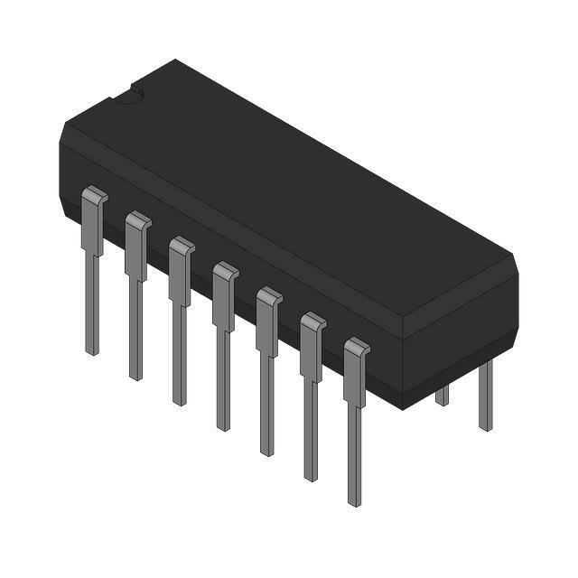
D, N, OR PW PACKAGE
(TOP VIEW)
1OUT
1IN –
1IN +
VDD
2IN +
2IN –
2OUT
1
14
2
13
3
12
4
11
5
10
6
9
7
8
4OUT
4IN –
4IN +
VDD – /GND
3IN +
2IN –
3OUT
description
symbol (each amplifier)
The TLC254, TLC254A, TLC254B, TLC25L4,
TLC254L4A, TLC254L4B, TLC25M4, TLC25M4A
+
IN +
and TL25M4B are low-cost, low-power quad
OUT
operational amplifiers designed to operate with
IN –
–
single or dual supplies. These devices utilize the
Texas Instruments silicon gate LinCMOS
process, giving them stable input-offset voltages that are available in selected grades of 2, 5, or 10 mV
maximum, very high input impedances, and extremely low input offset and bias currents. Because the input
common-mode range extends to the negative rail and the power consumption is extremely low, this series is
ideally suited for battery-powered or energy-conserving applications. The series offers operation down to a
1.4-V supply, is stable at unity gain, and has excellent noise characteristics.
These devices have internal electrostatic-discharge (ESD) protection circuits that prevent catastrophic failures
at voltages up to 2000 V as tested under MIL-STD-883C, Method 3015.1. However, care should be exercised
in handling these devices as exposure to ESD may result in degradation of the device parametric performance.
Because of the extremely high input impedance and low input bias and offset currents, applications for these
devices include many areas that have previously been limited to BIFET and NFET product types. Any circuit
using high-impedance elements and requiring small offset errors is a good candidate for cost-effective use of
these devices. Many features associated with bipolar technology are available with LinCMOS operational
amplifiers without the power penalties of traditional bipolar devices.
Available options
TA
0°C to 70°C
VIOmax
AT 25°C
PACKAGED DEVICES
SMALL OUTLINE
(D)
PLASTIC DIP
(N)
TSSOP
(PW)
CHIP FORM
(Y)
10 mV
5 mV
2 mV
TLC254CD
TLC254ACD
TLC254BCD
TLC254CN
TLC254ACN
TLC254BCN
TLC254CPW
—
—
TLC254Y
—
—
10 mV
5 mV
2 mV
TLC25L4CD
TLC25L4ACD
TLC25L2BCD
TLC25L4CN
TLC25L4ACN
TLC25L4BCN
TLC25L4CPW
—
—
TLC25L4Y
—
—
10 mV
5 mV
2 mV
TLC25M4CD
TLC25M4ACD
TLC25M4BCD
TLC25M4CN
TLC25M4ACN
TLC25M4BCN
TLC25M4CPW
—
—
TLC25M4Y
—
—
The D package is available taped and reeled. Add the suffix R to the device type (e.g., TLC254CDR). Chips
are tested at 25°C.
LinCMOS is a trademark of Texas Instruments.
Copyright 2001, Texas Instruments Incorporated
PRODUCTION DATA information is current as of publication date.
Products conform to specifications per the terms of Texas Instruments
standard warranty. Production processing does not necessarily include
testing of all parameters.
POST OFFICE BOX 655303
• DALLAS, TEXAS 75265
1
�TLC254, TLC254A, TLC254B, TLC254Y, TLC25L4, TLC25L4A, TLC25L4B
TLC25L4Y, TLC25M4, TLC25M4A, TLC25M4B, TLC25M4Y
LinCMOS QUAD OPERATIONAL AMPLIFIERS
SLOS003G – JUNE 1983 – REVISED MARCH 2001
description (continued)
General applications such as transducer interfacing, analog calculations, amplifier blocks, active filters, and
signal buffering are all easily designed with these devices. Remote and inaccessible equipment applications
are possible using their low-voltage and low-power capabilities. These devices are well suited to solve the
difficult problems associated with single-battery and solar-cell-powered applications. This series includes
devices that are characterized for the commercial temperature range and are available in 14-pin plastic dip and
the small-outline packages. The device is also available in chip form.
These devices are characterized for operation from 0°C to 70°C.
DEVICE FEATURES
TLC25L4_C
(LOW BIAS)
PARAMETER
TLC25M4_C
(MEDIUM BIAS)
TLC254_C
(HIGH BIAS)
40 µA
600 µA
4000 µA
0.04 V/µA
0.6 V/µA
4.5 V/µA
10 mV
5 mV
2 mV
10 mV
5 mV
2 mV
10 mV
5 mV
2 mV
0.1 µV/month†
0.1 µV/month†
0.1 µV/month†
0.7 µV/°C
2 µV/°C
5 µV/°C
1 pA
1 pA
1 pA
Input offset current (Typ)
1 pA
† The long-term drift value applies after the first month.
1 pA
1 pA
Supply current (Typ)
Slew rate (Typ)
Input offset voltage (Max)
TLC254C, TLC25L4C, TLC25M4C
TLC254AC, TLC25L4AC, TLC25M4AC
TLC254BC, TLC25L4BC, TLC25M4BC
Offset voltage drift (Typ)
Offset voltage temperature coefficient (Typ)
Input bias current (Typ)
equivalent schematic (each amplifier)
VDD
IN +
ESDProtective
Network
IN –
ESDProtective
Network
OUT
VDD – /GND
2
POST OFFICE BOX 655303
• DALLAS, TEXAS 75265
�TLC254, TLC254A, TLC254B, TLC254Y, TLC25L4, TLC25L4A, TLC25L4B
TLC25L4Y, TLC25M4, TLC25M4A, TLC25M4B, TLC25M4Y
LinCMOS QUAD OPERATIONAL AMPLIFIERS
SLOS003G – JUNE 1983 – REVISED MARCH 2001
chip information
These chips, when properly assembled, display characteristics similar to the TLC25_4C. Thermal compression
or ultrasonic bonding may be used on the doped-aluminum bonding pads. Chips may be mounted with
conductive epoxy or a gold-silicon preform.
BONDING PAD ASSIGNMENTS
VDD
(4)
(3)
+
1IN +
1IN –
(14)
(13)
(12) (11)
(10)
(9)
(1)
1OUT
(2)
–
(8)
(5)
+
(7)
2OUT
(10)
3IN +
2IN –
(8)
–
3IN –
4OUT
–
+
2IN +
3OUT
(9)
68
(6)
+
(14)
–
(12)
(13)
4IN +
4IN –
(11)
VDD– /GND
(1)
(2)
(3)
(4)
(5)
(6)
(7)
CHIP THICKNESS: 15 TYPICAL
BONDING PADS: 4 × 4 MINIMUM
108
TJmax = 150°C
TOLERANCES ARE ± 10%.
ALL DIMENSIONS ARE IN MILS.
PIN (11) IS INTERNALLY CONNECTED
TO BACKSIDE OF CHIP.
POST OFFICE BOX 655303
• DALLAS, TEXAS 75265
3
�TLC254, TLC254A, TLC254B, TLC254Y, TLC25L4, TLC25L4A, TLC25L4B
TLC25L4Y, TLC25M4, TLC25M4A, TLC25M4B, TLC25M4Y
LinCMOS QUAD OPERATIONAL AMPLIFIERS
SLOS003G – JUNE 1983 – REVISED MARCH 2001
absolute maximum ratings over operating free-air temperature range (unless otherwise noted)†
Supply voltage, VDD (see Note 1) . . . . . . . . . . . . . . . . . . . . . . . . . . . . . . . . . . . . . . . . . . . . . . . . . . . . . . . . . . . . 18 V
Differential input voltage (see Note 2) . . . . . . . . . . . . . . . . . . . . . . . . . . . . . . . . . . . . . . . . . . . . . . . . . . . . . . . . ± 18 V
Input voltage range (any input) . . . . . . . . . . . . . . . . . . . . . . . . . . . . . . . . . . . . . . . . . . . . . . . . . . . . . – 0.3 V to 18 V
Duration of short-circuit at (or below) 25°C free-air temperature (see Note 3) . . . . . . . . . . . . . . . . . . unlimited
Continuous total dissipation . . . . . . . . . . . . . . . . . . . . . . . . . . . . . . . . . . . . . . . . . . . See Dissipation Rating Table
Operating free-air temperature range . . . . . . . . . . . . . . . . . . . . . . . . . . . . . . . . . . . . . . . . . . . . . . . . . . 0°C to 70°C
Storage temperature range . . . . . . . . . . . . . . . . . . . . . . . . . . . . . . . . . . . . . . . . . . . . . . . . . . . . . . . . – 65°C to 150°C
Lead temperature 1,6 mm (1/16 inch) from case for 10 seconds . . . . . . . . . . . . . . . . . . . . . . . . . . . . . . . 260°C
† Stresses beyond those listed under “absolute maximum ratings” may cause permanent damage to the device. These are stress ratings only, and
functional operation of the device at these or any other conditions beyond those indicated under “recommended operating conditions” is not
implied. Exposure to absolute-maximum-rated conditions for extended periods may affect device reliability.
NOTES: 1. All voltage values, except differential voltages, are with respect to VDD – /GND.
2. Differential voltages are at IN+, with respect to IN –.
3. The output may be shorted to either supply. Temperature and/or supply voltages must be limited to ensure the maximum dissipation
rating is not exceeded.
DISSIPATION RATING TABLE
PACKAGE
TA ≤ 25°C
POWER RATING
DERATING FACTOR
ABOVE TA = 25°C
TA = 70°C
POWER RATING
D
725 mW
5.8 mW/°C
464 mW
N
1050 mW
9.2 mW/°C
736 mW
PW
700 mW
5.6 mW/°C
448 mW
recommended operating conditions
Supply voltage, VDD
Common mode input voltage,
Common-mode
voltage VIC
VDD = 1.4 V
VDD = 5 V
VDD = 10 V
VDD = 16 V
Operating free-air temperature, TA
4
POST OFFICE BOX 655303
• DALLAS, TEXAS 75265
MIN
MAX
1.4
16
0
0.2
– 0.2
4
– 0.2
9
– 0.2
14
0
70
UNIT
V
V
°C
�electrical characteristics at specified free-air temperature, VDD = 1.4 V (unless otherwise noted)
TLC25 4C
TLC25_4C
VIO
Input offset voltage
TLC254_C
TEST CONDITIONS†
PARAMETER
TLC25 4AC
TLC25_4AC
VO = 0
0.2
2V
V,
RS = 50 Ω
POST OFFICE BOX 655303 • DALLAS, TEXAS 75265
aVIO
Average
g temperature coefficient of
input offset voltage
IIO
Input offset current
2V
VO = 0
0.2
IIB
Input bias current
VO = 0
0.2
2V
VICR
Common-mode input voltage range
VOM
Peak output voltage swing‡
AVD
Large-signal differential voltage
amplification
CMRR
Common-mode rejection ratio
MIN
TYP
MIN
TYP
MAX
MIN
TYP
MAX
25°C
10
10
10
12
12
12
25°C
5
5
5
6.5
6.5
6.5
25°C
2
2
2
0°C to 70°C
3
3
3
0°C to 70°C
25°C to 70°C
1
25°C
1
25°C
1
60
1
0 to
0.2
25°C
450
25°C
60
1
450
1
60
60
600
0 to
0.2
700
450
20
77
60
300
60
0 to
0.2
700
1
600
10
60
60
77
60
UNIT
mV
µV/°C
1
300
600
25°C
25°C
1
300
0°C to 70°C
VO = 0.2 V,
VIC = VICRmin
VO = 0.2 V, No load
MAX
TLC25M4_C
0°C to 70°C
0°C to 70°C
VID = 100 mV
VO = 100 to 300 mV,
RS = 50 Ω
TLC25L4_C
pA
pA
V
700
mV
20
V/mV
77
dB
IDD
Supply current
25°C
600
750
50
68
400
500
µA
† All characteristics are measured under open-loop conditions with zero common-mode input voltage unless otherwise specified. Unless otherwise noted, an output load resistor is
connected from the output to ground and has the following value: for low bias, RL = 1 MΩ, for medium bias RL = 100 kΩ, and for high bias RL = 10 kΩ.
‡ The output swings to the potential of VDD – /GND.
PARAMETER
SR
B1
TEST CONDITIONS
Slew rate at unity gain
See Figure 1
Unity-gain bandwidth
AV = 40 dB,
RS = 50 Ω,
Overshoot factor
See Figure 1
CL = 10 pF,
See Figure 1
TLC254_C
MIN
TYP
TLC25L4_C
MAX
MIN
TYP
TLC25M4_C
MAX
MIN
TYP
MAX
UNIT
0.1
0.001
0.01
V/µs
12
12
12
kHz
30%
35%
35%
SLOS003G – JUNE 1983 – REVISED MARCH 2001
operating characteristics, VDD = 1.4 V, TA = 25°C
TLC254, TLC254A, TLC254B, TLC254Y, TLC25L4, TLC25L4A, TLC25L4B
TLC25L4Y, TLC25M4, TLC25M4A, TLC25M4B, TLC25M4Y
LinCMOSTM QUAD OPERATIONAL AMPLIFIERS
TLC25 4BC
TLC25_4BC
TA
5
�TLC254, TLC254A, TLC254B, TLC254Y, TLC25L4, TLC25L4A, TLC25L4B
TLC25L4Y, TLC25M4, TLC25M4A, TLC25M4B, TLC25M4Y
LinCMOS QUAD OPERATIONAL AMPLIFIERS
SLOS003G – JUNE 1983 – REVISED MARCH 2001
electrical characteristics at specified free-air temperature, VDD = 5 V (unless otherwise noted)
PARAMETER
TEST CONDITIONS
TA†
TLC254, TLC254AC,
TLC254BC
MIN
TLC254C
VIO
Input offset voltage
VO = 1.4 V,,
RS = 50 Ω,
VIC = 0,,
RL = 10 kΩ
25°C
VIC = 0,,
RL = 10 kΩ
Full range
TLC254BC
VO = 1.4 V,,
RS = 50 Ω,
VIC = 0,,
RL = 10 kΩ
Full range
IIO
Input offset current (see Note 4)
VO = 2
2.5
5V
V,
VIC = 2
2.5
5V
IIB
Input bias current (see Note 4)
VO = 2
2.5
5V
V,
VIC = 2
2.5
5V
VOL
AVD
CMRR
kSVR
IDD
Low-level output voltage
Large-signal
L
i
l differential
diff
ti l voltage
lt
am
lification
amplification
Common-mode rejection ratio
VID = 100 mV,
RL = 10 kΩ
VID = – 100 mV,
VO = 0.25 V to 2 V,
RL = 10 kΩ
VIC = VICRmin
Supply-voltage rejection ratio (∆VDD/∆VIO) VDD = 5 V to 10 V,
Supply current (four amplifiers)
IOL = 0
VO = 2
2.5
5V
V,
No load
VO = 1.4 V
VIC = 2
2.5
5V
V,
6.5
0.34
3
25°C
0.1
60
70°C
7
300
25°C
0.6
60
70°C
40
600
– 0.2
to
4
POST OFFICE BOX 655303
• DALLAS, TEXAS 75265
µV/°C
– 0.3
to
4.2
0°C
3
3.8
25°C
3.2
3.8
70°C
3
3.8
0
50
25°C
0
50
70°C
0
50
4
27
25°C
5
23
70°C
4
20
0°C
60
84
25°C
65
80
70°C
60
85
0°C
60
94
25°C
65
95
70°C
60
96
pA
V
0°C
0°C
pA
V
– 0.2
to
3.5
mV
V/mV
dB
dB
0°C
3.1
7.2
25°C
2.7
6.4
70°C
2.3
5.2
† Full range is 0°C to 70°C.
NOTES: 4. The typical values of input bias current and input offset current below 5 pA were determined mathematically.
5. This range also applies to each input individually.
6
mV
2
18
1.8
Common-mode input voltage
g range
g
(see Note 5)
High-level output voltage
5
25°C to
70°C
Full range
VOH
10
0.9
25°C
25°C
VICR
1.1
UNIT
12
25°C
VO = 1.4 V,,
RS = 50 Ω,
Average
g temperature coefficient of input
offset voltage
MAX
Full range
TLC254AC
αVIO
TYP
mA
�TLC254, TLC254A, TLC254B, TLC254Y, TLC25L4, TLC25L4A, TLC25L4B
TLC25L4Y, TLC25M4, TLC25M4A, TLC25M4B, TLC25M4Y
LinCMOS QUAD OPERATIONAL AMPLIFIERS
SLOS003G – JUNE 1983 – REVISED MARCH 2001
electrical characteristics at specified free-air temperature, VDD = 10 V (unless otherwise noted)
PARAMETER
TEST CONDITIONS
TA†
TLC254C, TLC254AC,
TLC254BC
MIN
VO = 1.4 V,,
RS = 50 Ω,
TLC254C
VIO
Input offset voltage
VIC = 0,,
RL = 10 kΩ
VIC = 0,,
RL = 10 kΩ
Full range
TLC254BC
VO = 1.4 V,,
RS = 50 Ω,
VIC = 0,,
RL = 10 kΩ
Full range
IIO
Input offset current (see Note 4)
VO = 5 V
V,
VIC = 5 V
IIB
Input bias current (see Note 4)
VO = 5 V
V,
VIC = 5 V
VOH
VOL
AVD
CMRR
kSVR
Low-level output voltage
Large-signal
L
i
l differential
diff
ti l voltage
lt
am
lification
amplification
Common-mode rejection ratio
Supply-voltage
S
l
lt
rejection
j ti ratio
ti
(∆VDD/∆VIO)
RL = 10 kΩ
VID = – 100 mV,
IOL = 0
VO = 1 V to 6 V,
RL = 10 kΩ
VIC = VICRmin
VDD = 5 V to 10 V,
VO = 1.4 V
5
6.5
0.39
2
µV/°C
2
25°C
0.1
60
70°C
7
300
25°C
0.7
60
70°C
50
600
25°C
– 0.2
to
9
Full range
– 0.2
to
8.5
– 0.3
to
9.2
0°C
7.8
8.5
25°C
8
8.5
70°C
7.8
8.4
0°C
0
50
0
50
70°C
0
50
0°C
7.5
42
10
36
70°C
7.5
32
0°C
60
88
25°C
65
85
70°C
60
88
0°C
60
94
25°C
65
95
70°C
60
dB
dB
96
8.8
25°C
3.8
8
70°C
3.2
† Full range is 0°C to 70°C.
NOTES: 4. The typical values of input bias current and input offset current below 5 pA were determined mathematically.
5. This range also applies to each input individually.
6.8
VO = 5 V
V,
No load
POST OFFICE BOX 655303
VIC = 5 V,
V
• DALLAS, TEXAS 75265
mV
V/mV
4.5
Supply current (four amplifiers)
pA
V
25°C
25°C
pA
V
0°C
IDD
mV
3
25°C to
70°C
VID = 100 mV,
10
0.9
25°C
Common-mode input voltage
g range
g
(see Note 5)
High-level output voltage
1.1
UNIT
12
25°C
VO = 1.4 V,,
RS = 50 Ω,
Average
g temperature coefficient of input
offset voltage
MAX
Full range
TLC254AC
∝VIO
VICR
25°C
TYP
mA
7
�TLC254, TLC254A, TLC254B, TLC254Y, TLC25L4, TLC25L4A, TLC25L4B
TLC25L4Y, TLC25M4, TLC25M4A, TLC25M4B, TLC25M4Y
LinCMOS QUAD OPERATIONAL AMPLIFIERS
SLOS003G – JUNE 1983 – REVISED MARCH 2001
operating characteristics, VDD = 5 V
PARAMETER
TEST CONDITIONS
TA
TLC254C, TLC254AC,
TLC254BC
MIN
VI(PP) = 1 V
SR
Slew rate at unity gain
RL = 10 kΩ,,
See Figure 1
CL = 20 pF,,
VI(PP) = 1 V
VI(PP)
( ) = 2.5 V
Vn
BOM
B1
φm
Equivalent input noise voltage
Maximum output-swing bandwidth
Unity-gain bandwidth
Phase margin
f = 1 kHz,
VO = VOH,
See Figure 1
VI = 10 mV,
VI = 10 mV,
mV
See Figure 3
RS = 20 Ω,
F
CL = 20 pF,
CL = 20 pF,
f = B1,
See Figure 2
RL = 10 kΩ,
kΩ
See Figure 1
CL = 20 pF,
pF
TYP
0°C
4
25°C
3.6
70°C
3
0°C
3.1
25°C
2.9
70°C
2.5
25°C
25
0°C
340
25°C
320
70°C
260
0°C
2
25°C
1.7
70°C
1.3
0°C
47°
25°C
46°
70°C
43°
UNIT
MAX
V/µs
nV/√Hz
kHz
MHz
operating characteristics, VDD = 10 V
PARAMETER
TEST CONDITIONS
TA
TLC254C, TLC254AC,
TLC254BC
MIN
VI(PP)
( )=1V
SR
Slew rate at unity gain
RL = 10 kΩ,,
See Figure 1
CL = 20 pF,,
VI(PP)
( ) = 5.5 V
Vn
BOM
B1
φm
8
Equivalent input noise voltage
Maximum output-swing bandwidth
Unity-gain bandwidth
Phase margin
f = 1 kHz,
VO = VOH,
See Figure 1
VI = 10 mV,
mV
VI = 10 mV,
See Figure 3
RS = 20 Ω,
CL = 20 pF,
F
CL = 20 pF,
f = B1,
POST OFFICE BOX 655303
See Figure 2
RL = 10 kΩ,
kΩ
See Figure 1
pF
CL = 20 pF,
• DALLAS, TEXAS 75265
TYP
0°C
5.9
25°C
5.3
70°C
4.3
0°C
5.1
25°C
4.6
70°C
3.8
25°C
25
0°C
220
25°C
200
70°C
140
0°C
2.5
25°C
2.2
70°C
1.8
0°C
50°
25°C
49°
70°C
46°
UNIT
MAX
V/µs
nV/√Hz
kHz
MHz
�TLC254, TLC254A, TLC254B, TLC254Y, TLC25L4, TLC25L4A, TLC25L4B
TLC25L4Y, TLC25M4, TLC25M4A, TLC25M4B, TLC25M4Y
LinCMOS QUAD OPERATIONAL AMPLIFIERS
SLOS003G – JUNE 1983 – REVISED MARCH 2001
electrical characteristics at specified free-air temperature, VDD = 5 V (unless otherwise noted)
PARAMETER
TEST CONDITIONS
TA†
TLC25L4C
TLC25L4AC
TLC25L4BC
MIN
VIO
Input offset voltage
TLC25L4C
VO = 1.4 V,,
RS = 50 Ω,
VIC = 0,,
RL = 1 MΩ
Full range
TLC25L4AC
VO = 1.4 V,,
RS = 50 Ω,
VIC = 0,,
RL = 1 MΩ
Full range
TLC25L4BC
VO = 1.4 V,,
RS = 50 Ω,
VIC = 0,,
RL = 1 MΩ
∝VIO
Average
g temperature coefficient of input
offset voltage
IIO
Input offset current (see Note 4)
VO = 2
2.5
5V
V,
VIC = 2
2.5
5V
IIB
Input bias current (see Note 4)
VO = 2
2.5
5V
V,
VIC = 2
2.5
5V
VICR
VOH
VOL
25°C
Low-level output voltage
VID = 100 mV,
RL = 1 MΩ
VID = – 100 mV,
IOL = 0
CMRR
kSVR
Large-signal
L
i
l differential
diff
ti l voltage
lt
amplification
am
lification
Common-mode rejection ratio
S
l
lt
j ti ratio
ti
Supply-voltage
rejection
(∆VDD/∆VIO)
VO = 0.25 V to 2 V,
RL = 1 MΩ
VIC = VICRmin
VDD = 5 V to 10 V,
VO = 1.4 V
MAX
1.1
10
0.9
5
6.5
25°C
0.24
Full range
3
11
1.1
25°C
0.1
60
70°C
7
300
25°C
0.6
60
70°C
40
600
25°C
– 0.2
to
4
Full range
– 0.2
to
3.5
µV/°C
– 0.3
to
4.2
0°C
3
4.1
25°C
3.2
4.1
70°C
3
4.2
V
0°C
0
50
25°C
0
50
0
50
0°C
50
680
25°C
50
520
70°C
50
380
0°C
60
95
25°C
65
94
70°C
60
95
0°C
60
97
25°C
70
98
70°C
60
97
dB
dB
25°C
40
68
70°C
31
† Full range is 0°C to 70°C.
NOTES: 4. The typical values of input bias current and input offset current below 5 pA were determined mathematically.
5. This range also applies to each input individually.
56
POST OFFICE BOX 655303
VIC = 2
2.5
5V
V,
• DALLAS, TEXAS 75265
mV
V/mV
84
VO = 2
2.5
5V
V,
No load
pA
V
48
Supply current (four amplifiers)
pA
V
0°C
IDD
mV
2
25°C to
70°C
70°C
AVD
TYP
12
25°C
Common-mode input voltage
g range
g
(see Note 5)
High-level output voltage
UNIT
µA
9
�TLC254, TLC254A, TLC254B, TLC254Y, TLC25L4, TLC25L4A, TLC25L4B
TLC25L4Y, TLC25M4, TLC25M4A, TLC25M4B, TLC25M4Y
LinCMOS QUAD OPERATIONAL AMPLIFIERS
SLOS003G – JUNE 1983 – REVISED MARCH 2001
electrical characteristics at specified free-air temperature, VDD = 10 V (unless otherwise noted)
PARAMETER
TEST CONDITIONS
TA†
TLC25L4C
TLC25L4AC
TLC25L4BC
MIN
VIO
Input offset voltage
TLC25L4C
VO = 1.4 V,,
RS = 50 Ω,
VIC = 0,,
RL = 1 MΩ
Full range
TLC25L4AC
VO = 1.4 V,,
RS = 50 Ω,
VIC = 0,,
RL = 1 MΩ
Full range
TLC25L4BC
VO = 1.4 V,,
RS = 50 Ω,
VIC = 0,,
RL = 1 MΩ
αVIO
Average
g temperature coefficient of
input offset voltage
IIO
Input offset current (see Note 4)
VO = 5 V
V,
VIC = 5 V
IIB
Input bias current (see Note 4)
VO = 5 V
V,
VIC =
5V
=.5
VICR
25°C
VOL
AVD
CMRR
kSVR
IDD
Low-level output voltage
Large-signal
L
i
l diff
differential
ti l voltage
lt
am
lification
amplification
Common-mode rejection ratio
RL = 1 MΩ
VID = – 100 mV,
VO = 1 V to 6 V,
IOL = 0
RL = 1 MΩ
VIC = VICRmin
S
l
lt
j ti ratio
ti
Supply-voltage
rejection
(∆VDD/∆VIO)
VDD = 5 V to 10 V,
Supply current (four amplifiers)
VO = 5 V
V,
No load
VO = 1.4 V
VIC = 5 V,
V
10
0.26
Full range
POST OFFICE BOX 655303
• DALLAS, TEXAS 75265
mV
2
3
µV/°C
1
25°C
0.1
60
70°C
7
300
25°C
0.7
60
70°C
50
600
25°C
– 0.2
to
9
Full range
– 0.2
to
8.5
– 0.3
to
9.2
pA
pA
V
V
7.8
8.9
25°C
8
8.9
70°C
7.8
8.9
V
0°C
0
50
25°C
0
50
70°C
0
50
0°C
50
1025
25°C
50
870
70°C
50
660
0°C
60
97
25°C
65
97
70°C
60
97
0°C
60
97
25°C
70
97
70°C
60
98
mV
V/mV
dB
dB
0°C
72
132
25°C
57
92
70°C
44
80
† Full range is 0°C to 70°C.
NOTES: 4. The typical values of input bias current and input offset current below 5 pA were determined mathematically.
5. This range also applies to each input individually.
10
5
6.5
25°C to
70°C
VID = 100 mV,
MAX
1.1
0.9
25°C
Common-mode input voltage
g range
g ((see
Note 5)
High-level output voltage
TYP
12
25°C
0°C
VOH
UNIT
µA
�TLC254, TLC254A, TLC254B, TLC254Y, TLC25L4, TLC25L4A, TLC25L4B
TLC25L4Y, TLC25M4, TLC25M4A, TLC25M4B, TLC25M4Y
LinCMOS QUAD OPERATIONAL AMPLIFIERS
SLOS003G – JUNE 1983 – REVISED MARCH 2001
operating characteristics, VDD = 5 V
PARAMETER
TEST CONDITIONS
TA
TLC25L4C
TLC25L4AC
TLC25L4BC
MIN
VI(PP)
( )=1V
SR
Slew rate at unity gain
RL = 1 MΩ,,
See Figure 1
CL = 20 pF,,
VI(PP)
( ) = 2.5 V
TYP
0°C
0.04
25°C
0.03
70°C
0.03
0°C
0.03
25°C
0.03
70°C
0.02
Vn
Equivalent input noise voltage
f = 1 kHz,
RS = 20 Ω,
See Figure 2
25°C
70
0°C
6
BOM
Maximum output-swing bandwidth
VO = VOH,
See Figure 1
CL = 20 pF,
F
RL = 1 MΩ,
MΩ
25°C
5
B1
φm
Unity-gain bandwidth
Phase margin
VI = 10 mV,
CL = 20 pF,
VI = 10 mV,
mV
See Figure 3
f = B1,
See Figure 1
CL = 20 pF
pF,
70°C
4.5
0°C
100
25°C
85
70°C
65
0°C
36°
25°C
34°
70°C
30°
UNIT
MAX
V/µs
nV/√Hz
kHz
kHz
operating characteristics, VDD = 10 V
PARAMETER
TEST CONDITIONS
TA
TLC25L4C
TLC25L4AC
TLC25L4BC
MIN
VI(PP)
( )=1V
SR
Slew rate at unity gain
RL = 1 MΩ,,
See Figure 1
CL = 20 pF,,
VI(PP)
( ) = 5.5 V
TYP
0°C
0.05
25°C
0.05
70°C
0.04
0°C
0.05
25°C
0.04
70°C
0.04
Vn
Equivalent input noise voltage
f = 1 kHz,
RS = 20 Ω,
See Figure 2
25°C
70
0°C
1.3
BOM
Maximum output-swing bandwidth
VO = VOH,
See Figure 1
CL = 20 pF,
F
RL = 1 MΩ,
MΩ
25°C
1
70°C
0.9
B1
φm
Unity-gain bandwidth
Phase margin
VI = 10 mV,
VI = 10 mV,
mV
See Figure 3
CL = 20 pF,
f = B1,
POST OFFICE BOX 655303
See Figure 1
CL = 20 pF
pF,
• DALLAS, TEXAS 75265
0°C
125
25°C
110
70°C
90
0°C
40°
25°C
38°
70°C
34°
UNIT
MAX
V/µs
nV/√Hz
kHz
kHz
11
�TLC254, TLC254A, TLC254B, TLC254Y, TLC25L4, TLC25L4A, TLC25L4B
TLC25L4Y, TLC25M4, TLC25M4A, TLC25M4B, TLC25M4Y
LinCMOS QUAD OPERATIONAL AMPLIFIERS
SLOS003G – JUNE 1983 – REVISED MARCH 2001
electrical characteristics at specified free-air temperature, VDD = 5 V (unless otherwise noted)
PARAMETER
TEST CONDITIONS
TA†
TLC25M4C
TLC25M4AC
TLC25M4BC
MIN
VIO
Input offset voltage
TLC25M4C
VO = 1.4 V,,
RS = 50 Ω,
VIC = 0,,
RL = 100 kΩ
Full range
TLC25M4AC
VO = 1.4 V,,
RS = 50 Ω,
VIC = 0,,
RL = 100 kΩ
Full range
TLC25M4BC
VO = 1.4 V,,
RS = 50 Ω,
VIC = 0,,
RL = 100 kΩ
∝VIO
Average
g temperature coefficient of
input offset voltage
IIO
Input offset current (see Note 4)
VO = 2
2.5
5V
V,
VIC = 2
2.5
5V
IIB
Input bias current (see Note 4)
VO = 2
2.5
5V
V,
VIC = 2
2.5
5V
VICR
VOH
VOL
AVD
CMRR
kSVR
IDD
25°C
Low-level output voltage
Large-signal
L
i
l differential
diff
ti l voltage
lt
am
lification
amplification
Common-mode rejection ratio
VID = 100 mV,
RL = 100 kΩ
VID = – 100 mV,
IOL = 0
VO = 0.25 V to 2 V,
RL = 100 kΩ
VIC = VICRmin
S
l
lt
j ti ratio
ti
Supply-voltage
rejection
(∆VDD/∆VIO)
VDD = 5 V to 10 V,
Supply current (four amplifiers)
VO = 2
2.5
5V
V,
No load
VO = 1.4 V
VIC = 2
2.5
5V
V,
TYP
MAX
1.1
10
12
25°C
0.9
0.25
Full range
POST OFFICE BOX 655303
• DALLAS, TEXAS 75265
mV
2
3
25°C to
70°C
17
1.7
25°C
0.1
60
70°C
7
300
25°C
0.6
60
70°C
40
600
25°C
– 0.2
t0
4
Full range
– 0.2
to
3.5
µV/°C
– 0.3
to
4.2
pA
pA
V
V
0°C
3
3.9
25°C
3.2
3.9
70°C
3
4
V
0°C
0
50
25°C
0
50
70°C
0
50
0°C
15
200
25°C
25
170
70°C
15
140
0°C
60
91
25°C
65
91
70°C
60
92
0°C
60
92
25°C
70
93
70°C
60
94
mV
V/mV
dB
dB
0°C
500
1280
25°C
420
1120
70°C
340
880
† Full range is 0°C to 70°C.
NOTES: 4. The typical values of input bias current and input offset current below 5 pA were determined mathematically.
5. This range also applies to each input individually.
12
5
6.5
25°C
Common-mode input voltage
g range
g
(see Note 5)
High-level output voltage
UNIT
µA
�TLC254, TLC254A, TLC254B, TLC254Y, TLC25L4, TLC25L4A, TLC25L4B
TLC25L4Y, TLC25M4, TLC25M4A, TLC25M4B, TLC25M4Y
LinCMOS QUAD OPERATIONAL AMPLIFIERS
SLOS003G – JUNE 1983 – REVISED MARCH 2001
electrical characteristics at specified free-air temperature, VDD = 10 V (unless otherwise noted)
PARAMETER
TEST CONDITIONS
TA†
TLC25M4C
TLC25M4AC
TLC25M4BC
MIN
VIO
Input offset voltage
TLC25M4C
VO = 1.4 V,,
RS = 50 Ω,
VIC = 0,,
RL = 100 kΩ
Full range
TLC25M4AC
VO = 1.4 V,,
RS = 50 Ω,
VIC = 0,,
RL = 100 kΩ
Full range
TLC25M4BC
VO = 1.4 V,,
RS = 50 Ω,
VIC = 0,,
RL = 100 kΩ
αVIO
Average
g temperature coefficient of input
offset voltage
IIO
Input offset current (see Note 4)
VO = 5 V
V,
VIC = 5 V
IIB
Input bias current (see Note 4)
VO = 5 V
V,
VIC = 5 V
VICR
25°C
VOL
AVD
CMRR
kSVR
IDD
VID = 100 mV,
Low-level output voltage
VID = – 100 mV,
Large-signal
L
i
l differential
diff
ti l voltage
lt
am
lification
amplification
VO = 1 V to 6 V,
Common-mode rejection ratio
IOL = 0
RL = 100 kΩ
VIC = VICRmin
Supply-voltage rejection ratio (∆VDD/∆VIO)
Supply current (four amplifiers)
RL = 100 kΩ
VDD = 5 V to 10 V,
VO = 5 V
V,
No load
VO = 1.4 V
VIC = 5 V,
V
MAX
1.1
10
0.9
5
6.5
25°C
0.26
Full range
mV
2
3
25°C to
70°C
21
2.1
25°C
0.1
60
70°C
7
300
25°C
0.7
60
70°C
50
600
25°C
– 0.2
to
9
Full range
– 0.2
to
8.5
Common-mode input voltage
g range
g ((see
Note 5)
High-level output voltage
TYP
12
25°C
0°C
VOH
UNIT
µV/°C
– 0.3
to
9.2
pA
pA
V
V
7.8
8.7
25°C
8
8.7
70°C
7.8
8.7
V
0°C
0
50
25°C
0
50
70°C
0
50
0°C
15
320
25°C
25
275
70°C
15
230
0°C
60
94
25°C
65
94
70°C
60
94
0°C
60
92
25°C
70
93
70°C
60
94
mV
V/mV
dB
dB
0°C
690
1600
25°C
570
1200
70°C
440
1120
µA
† Full range is 0°C to 70°C.
NOTES: 4. The typical values of input bias current and input offset current below 5 pA were determined mathematically.
5. This range also applies to each input individually.
POST OFFICE BOX 655303
• DALLAS, TEXAS 75265
13
�TLC254, TLC254A, TLC254B, TLC254Y, TLC25L4, TLC25L4A, TLC25L4B
TLC25L4Y, TLC25M4, TLC25M4A, TLC25M4B, TLC25M4Y
LinCMOS QUAD OPERATIONAL AMPLIFIERS
SLOS003G – JUNE 1983 – REVISED MARCH 2001
operating characteristics, VDD = 5 V
PARAMETER
TEST CONDITIONS
TA
TLC25M4C
TLC25M4AC
TLC25M4BC
MIN
VI(PP) = 1 V
SR
Slew rate at unity gain
RL = 100 kΩ,,
See Figure 1
CL = 20 pF,,
VI(PP)
( ) = 2.5 V
TYP
0.46
V/µs
25°C
0.43
V/µs
70°C
0.36
0°C
0.43
25°C
0.40
70°C
0.34
Equivalent input noise voltage
f = 1 kHz,
RS = 20 Ω,
See Figure 2
25°C
32
0°C
60
BOM
Maximum output-swing bandwidth
VO = VOH,
See Figure 1
CL = 20 pF,
F
RL = 100 kΩ,
kΩ
25°C
55
φm
Unity-gain bandwidth
Phase margin
VI = 10 mV,
CL = 20 pF,
VI = 10 mV,
mV
See Figure 3
f = B1,
See Figure 1
CL = 20 pF,
pF
MAX
0°C
Vn
B1
UNIT
70°C
50
0°C
610
25°C
525
70°C
400
0°C
41°
25°C
40°
70°C
39°
V/µs
nV/√Hz
kHz
kHz
operating characteristics, VDD = 10 V
PARAMETER
TEST CONDITIONS
TA
TLC25M4C
TLC25M4AC
TLC25M4BC
MIN
VI(PP)
( )=1V
SR
Slew rate at unity gain
RL = 100 kΩ,,
See Figure 1
CL = 20 pF,,
VI(PP)
( ) = 5.5 V
TYP
0°C
0.67
25°C
0.62
70°C
0.51
0°C
0.61
25°C
0.56
70°C
0.46
Vn
Equivalent input noise voltage
f = 1 kHz,
RS = 20 Ω,
See Figure 2
25°C
32
0°C
40
BOM
Maximum output-swing bandwidth
VO = VOH,
See Figure 1
CL = 20 pF,
F
RL = 100 kΩ,
kΩ
25°C
35
70°C
30
B1
φm
14
Unity-gain bandwidth
Phase margin
VI = 10 mV,
VI = 10 mV,
mV
See Figure 3
CL = 20 pF,
f = B1,
POST OFFICE BOX 655303
See Figure 1
CL = 20 pF,
pF
• DALLAS, TEXAS 75265
0°C
710
25°C
635
70°C
510
0°C
44°
25°C
43°
70°C
42°
UNIT
MAX
V/µs
nV/√Hz
kHz
kHz
�TLC254, TLC254A, TLC254B, TLC254Y, TLC25L4, TLC25L4A, TLC25L4B
TLC25L4Y, TLC25M4, TLC25M4A, TLC25M4B, TLC25M4Y
LinCMOS QUAD OPERATIONAL AMPLIFIERS
SLOS003G – JUNE 1983 – REVISED MARCH 2001
electrical characteristics, VDD = 5 V, TA = 25°C (unless otherwise noted)
TEST
CONDITIONS
PARAMETER
TLC254Y
MIN
VO = 1.4 V,
VIC = 0 V,
RS = 50 Ω,
See Note 6
TLC25L4Y
TYP
MAX
1.1
10
MIN
TLC25M4Y
TYP
MAX
1.1
10
MIN
TYP
MAX
1.1
10
UNIT
VIO
Input offset voltage
αVIO
Average temperature
coefficient of input
offset voltage
IIO
Input offset current
(see Note 4)
VO = VDD/2,
VIC = VDD/2
0.1
60
0.1
60
0.1
60
pA
IIB
Input bias current
(see Note 4)
VO = VDD/2,
VIC = VDD/2
0.6
60
0.6
60
0.6
60
pA
VICR
Common-mode input
voltage range
(see Note 5)
VOH
High-level output
voltage
VOL
Low-level output voltage
AVD
Large-signal differential
voltage amplification
VO = 0.25 V,
See Note 6
CMRR
Common-mode rejection
ratio
kSVR
IDD
1.8
VID = 100 mV,
RL = 100 kΩ
VID = – 100 mV,
IOL = 0
1.1
mV
µV/°C
1.7
– 0.2
to
4
– 0.3
to
4.2
– 0.2
to
4
– 0.3
to
4.2
– 0.2
to
4
– 0.3
to
4.2
V
3.2
3.8
3.2
4.1
3.2
3.9
V
0
50
0
50
0
50
mV
5
23
50
520
25
170
V/mV
VIC = VICRmin
65
80
65
94
65
91
dB
Supply-voltage rejection
ratio (∆VDD/∆VIO)
VDD = 5 V to 10 V,
VO = 1.4 V
65
95
70
97
70
93
dB
Supply current
VO = VDD/2,
VIC = VDD/2,
No load
2.7
6.4
0.04
0.068
0.42
1.12
mA
NOTES: 4. The typical values of input bias current and input offset current below 5 pA were determined mathematically.
5. This range also applies to each input individually.
6. For low-bias mode, RL = 1 MΩ, for medium-bias mode, RL = 100 kΩ, and for high-bias mode, RL = 10 kΩ.
operating characteristics, VDD = 5 V, TA = 25°C
PARAMETER
TEST CONDITIONS
TLC254Y
MIN
TYP
TLC25L4Y
MAX
MIN
TYP
TLC25M4Y
MAX
MIN
TYP
MAX
UNIT
SR
Slew rate at
unity gain
CL = 20 pF,,
See Note 6
VI(PP) = 1 V
VI(PP) = 2.5 V
3.6
0.03
0.43
2.9
0.03
0.40
Vn
Equivalent
input noise
voltage
f = 1 kHz,
RS = 20 Ω
2.5
70
32
nV/√Hz
BOM
Maximum
output-swing
bandwidth
VO = VOH,
RL = 10 kΩ
CL = 20 pF,
320
5
55
kHz
B1
Unity-gain
bandwidth
VI = 10 mV,
CL = 20 pF
1.7
0.085
0.525
MHz
φm
Phase margin
f = B1,
CL = 20 pF
VI = 10 mV,
46°
34°
40°
V/µs
NOTE 6: For low-bias mode, RL = 1 MΩ, for medium-bias mode, RL = 100 kΩ, and for high-bias mode, RL = 10 kΩ.
POST OFFICE BOX 655303
• DALLAS, TEXAS 75265
15
�TLC254, TLC254A, TLC254B, TLC254Y, TLC25L4, TLC25L4A, TLC25L4B
TLC25L4Y, TLC25M4, TLC25M4A, TLC25M4B, TLC25M4Y
LinCMOS QUAD OPERATIONAL AMPLIFIERS
SLOS003G – JUNE 1983 – REVISED MARCH 2001
PARAMETER MEASUREMENT INFORMATION
single-supply versus split-supply test circuits
Because the TLC25_4, TLC25_4A, and TLC25_4B are optimized for single-supply operation, circuit
configurations used for the various tests often present some inconvenience since the input signal, in many
cases, must be offset from ground. This inconvenience can be avoided by testing the device with split supplies
and the output load tied to the negative rail. A comparison of single-supply versus split-supply test circuits is
shown below. The use of either circuit gives the same result.
VDD
VDD +
–
VO
+
VI
CL
–
VO
+
VI
CL
RL
RL
VDD –
(b) SPLIT-SUPPLY
(a) SINGLE-SUPPLY
Figure 1. Unity-Gain Amplifier
2 kΩ
2 kΩ
VDD +
VDD
20 Ω
–
1/2 VDD
–
VO
+
+
VO
20 Ω
20 Ω
20 Ω
VDD –
(a) SINGLE-SUPPLY
(b) SPLIT-SUPPLY
Figure 2. Noise-Test Circuit
10 kΩ
10 kΩ
VDD +
VDD
100 Ω
VI
–
1/2 VDD
+
VO
VI
100 Ω
–
+
CL
CL
VDD –
(a) SINGLE-SUPPLY
(b) SPLIT-SUPPLY
Figure 3. Gain-of-100 Inverting Amplifier
16
POST OFFICE BOX 655303
VO
• DALLAS, TEXAS 75265
�TLC254, TLC254A, TLC254B, TLC254Y, TLC25L4, TLC25L4A, TLC25L4B
TLC25L4Y, TLC25M4, TLC25M4A, TLC25M4B, TLC25M4Y
LinCMOS QUAD OPERATIONAL AMPLIFIERS
SLOS003G – JUNE 1983 – REVISED MARCH 2001
TYPICAL CHARACTERISTICS
Table of Graphs
FIGURE
IDD
Supply current
AVD
Large-signal differential voltage amplification
Phase shift
vs Supplyy voltage
g
vs Free-air temperature
4
5
Low bias
vs Frequency
6
Medium bias
vs Frequency
7
High bias
vs Frequency
8
Low bias
vs Frequency
6
Medium bias
vs Frequency
7
High bias
vs Frequency
8
SUPPLY CURRENT
vs
FREE-AIR TEMPERATURE
SUPPLY CURRENT
vs
SUPPLY VOLTAGE
10000
10000
High-Bias Versions
High-Bias Versions
xA
A
IICC
DD – Supply Current – µ
xA
A
IICC
DD – Supply Current – µ
VO = VIC = 0.2 VDD
No Load
TA = 25°C
1000
Medium-Bias Versions
100
Low-Bias Versions
10
VDD = 10 V
VIC = 0
VO = 2 V
No Load
1000
Medium-Bias Versions
100
Low-Bias Versions
10
0
0
0
2
4
6
8
10 12 14 16
VDD – Supply Voltage – V
18
20
0
10
20
30
40
50
60
TA – Free-Air Temperature – °C
70
80
Figure 5
Figure 4
POST OFFICE BOX 655303
• DALLAS, TEXAS 75265
17
�TLC254, TLC254A, TLC254B, TLC254Y, TLC25L4, TLC25L4A, TLC25L4B
TLC25L4Y, TLC25M4, TLC25M4A, TLC25M4B, TLC25M4Y
LinCMOS QUAD OPERATIONAL AMPLIFIERS
SLOS003G – JUNE 1983 – REVISED MARCH 2001
TYPICAL CHARACTERISTICS
LOW-BIAS LARGE-SIGNAL DIFFERENTIAL
VOLTAGE AMPLIFICATION AND PHASE SHIFT
vs
FREQUENCY
ÁÁ
ÁÁ
ÁÁ
VDD = 10 V
RL = 1 MΩ
TA = 25°C
106
105
0°
30°
AVD (left scale)
104
60°
103
102
90°
Phase Shift
(right scale)
120°
101
150°
1
180°
0.1
0.1
1
Phase Shift
AVD
AVD – Low-Bias Large-Signal Differential
Voltage Amplification
107
10
100
1k
10 k
100 k
Frequency – Hz
Figure 6
MEDIUM-BIAS LARGE-SIGNAL
DIFFERENTIAL VOLTAGE AMPLIFICATION
AND PHASE SHIFT
vs
FREQUENCY
ÁÁ
ÁÁ
VDD = 10 V
RL = 100 kΩ
TA = 25°C
106
105
30°
AVD (left scale)
104
60°
103
102
90°
Phase Shift
(right scale)
120°
101
150°
1
180°
0.1
1
10
100
1k
10 k
Frequency – Hz
100 k
Figure 7
18
0°
POST OFFICE BOX 655303
• DALLAS, TEXAS 75265
1M
Phase Shift
AVD
A
VD – Medium-Bias Large-Signal Differential
Voltage Amplification
107
�TLC254, TLC254A, TLC254B, TLC254Y, TLC25L4, TLC25L4A, TLC25L4B
TLC25L4Y, TLC25M4, TLC25M4A, TLC25M4B, TLC25M4Y
LinCMOS QUAD OPERATIONAL AMPLIFIERS
SLOS003G – JUNE 1983 – REVISED MARCH 2001
TYPICAL CHARACTERISTICS
HIGH-BIAS LARGE-SIGNAL
DIFFERENTIAL VOLTAGE AMPLIFICATION
AND PHASE SHIFT
vs
FREQUENCY
ÁÁ
ÁÁ
VDD = 10 V
RL = 10 kΩ
TA = 25°C
106
105
0°
30°
104
60°
Phase Shift (right scale)
103
90°
AVD (left scale)
102
120°
101
150°
1
180°
0.1
10
100
1k
10 k
100 k
1M
Phase Shift
AVD
AVD – High-Bias Large-Signal Differential
Voltage Amplification
107
10 M
Frequency – Hz
Figure 8
POST OFFICE BOX 655303
• DALLAS, TEXAS 75265
19
�TLC254, TLC254A, TLC254B, TLC254Y, TLC25L4, TLC25L4A, TLC25L4B
TLC25L4Y, TLC25M4, TLC25M4A, TLC25M4B, TLC25M4Y
LinCMOS QUAD OPERATIONAL AMPLIFIERS
SLOS003G – JUNE 1983 – REVISED MARCH 2001
APPLICATION INFORMATION
latch-up avoidance
Junction-isolated CMOS circuits have an inherent parasitic PNPN structure that can function as an SCR. Under
certain conditions, this SCR may be triggered into a low-impedance state, resulting in excessive supply current.
To avoid such conditions, no voltage greater than 0.3 V beyond the supply rails should be applied to any pin.
In general, the operational amplifiers supplies should be established simultaneously with, or before, application
of any input signals.
output stage considerations
The amplifier’s output stage consists of a source-follower-connected pullup transistor and an open-drain
pulldown transistor. The high-level output voltage (VOH) is virtually independent of the IDD selection and
increases with higher values of VDD and reduced output loading. The low-level output voltage (VOL) decreases
with reduced output current and higher input common-mode voltage. With no load, VOL is essentially equal to
the potential of VDD – /GND.
supply configurations
Even though the TLC25_4C series is are characterized for single-supply operation, they can be used effectively
in a split-supply configuration if the input common-mode voltage (VICR), output swing (VOL and VOH), and supply
voltage limits are not exceeded.
circuit layout precautions
Whenever extremely high circuit impedances are used, care must be exercised in layout, construction, board
cleanliness, and supply filtering to avoid hum and noise pickup as well as excessive dc leakages.
20
POST OFFICE BOX 655303
• DALLAS, TEXAS 75265
�PACKAGE OPTION ADDENDUM
www.ti.com
14-Aug-2021
PACKAGING INFORMATION
Orderable Device
Status
(1)
Package Type Package Pins Package
Drawing
Qty
Eco Plan
(2)
Lead finish/
Ball material
MSL Peak Temp
Op Temp (°C)
Device Marking
(3)
(4/5)
(6)
TLC254ACD
ACTIVE
SOIC
D
14
50
RoHS & Green
NIPDAU
Level-1-260C-UNLIM
0 to 70
TLC254AC
TLC254BCD
ACTIVE
SOIC
D
14
50
RoHS & Green
NIPDAU
Level-1-260C-UNLIM
0 to 70
TLC254BC
TLC254BCN
ACTIVE
PDIP
N
14
25
RoHS & Green
NIPDAU
N / A for Pkg Type
0 to 70
TLC254BCN
TLC254CD
ACTIVE
SOIC
D
14
50
RoHS & Green
NIPDAU
Level-1-260C-UNLIM
0 to 70
TLC254C
TLC254CDG4
ACTIVE
SOIC
D
14
50
RoHS & Green
NIPDAU
Level-1-260C-UNLIM
0 to 70
TLC254C
TLC254CN
ACTIVE
PDIP
N
14
25
RoHS & Green
NIPDAU
N / A for Pkg Type
0 to 70
TLC254CN
TLC254CNE4
ACTIVE
PDIP
N
14
25
RoHS & Green
NIPDAU
N / A for Pkg Type
0 to 70
TLC254CN
TLC25L4BCD
ACTIVE
SOIC
D
14
50
RoHS & Green
NIPDAU
Level-1-260C-UNLIM
0 to 70
25L4BC
TLC25L4BCN
ACTIVE
PDIP
N
14
25
RoHS & Green
NIPDAU
N / A for Pkg Type
TLC25L4CD
ACTIVE
SOIC
D
14
50
RoHS & Green
NIPDAU
Level-1-260C-UNLIM
0 to 70
TLC25L4C
TLC25L4CDG4
ACTIVE
SOIC
D
14
50
RoHS & Green
NIPDAU
Level-1-260C-UNLIM
0 to 70
TLC25L4C
TLC25M4CD
ACTIVE
SOIC
D
14
50
RoHS & Green
NIPDAU
Level-1-260C-UNLIM
0 to 70
TLC25M4C
TLC25M4CN
ACTIVE
PDIP
N
14
25
RoHS & Green
NIPDAU
N / A for Pkg Type
0 to 70
TLC25M4CN
TLC25L4BCN
(1)
The marketing status values are defined as follows:
ACTIVE: Product device recommended for new designs.
LIFEBUY: TI has announced that the device will be discontinued, and a lifetime-buy period is in effect.
NRND: Not recommended for new designs. Device is in production to support existing customers, but TI does not recommend using this part in a new design.
PREVIEW: Device has been announced but is not in production. Samples may or may not be available.
OBSOLETE: TI has discontinued the production of the device.
(2)
RoHS: TI defines "RoHS" to mean semiconductor products that are compliant with the current EU RoHS requirements for all 10 RoHS substances, including the requirement that RoHS substance
do not exceed 0.1% by weight in homogeneous materials. Where designed to be soldered at high temperatures, "RoHS" products are suitable for use in specified lead-free processes. TI may
reference these types of products as "Pb-Free".
RoHS Exempt: TI defines "RoHS Exempt" to mean products that contain lead but are compliant with EU RoHS pursuant to a specific EU RoHS exemption.
Green: TI defines "Green" to mean the content of Chlorine (Cl) and Bromine (Br) based flame retardants meet JS709B low halogen requirements of


 工商网监
湘ICP备2023018690号
工商网监
湘ICP备2023018690号
