www.ti.com
��������� ��������� ������� � ������
�� �������� �
�� ����� ������
����� ��� ����� ��� ����� � � �����
�� ����� �� �
�� �� ������
����������������������� ������ ����������� ������ ����������
SLVS230G − SEPTEMBER 1999 − REVISED JANUARY 2004
D Open Drain Power-On Reset With 200 ms
D
D
D
D
D
D
D
D
D
Delay (TPS777xx)
Open Drain Power Good (TPS778xx)
750-mA Low-Dropout Voltage Regulator
Available in 1.5-V, 1.8-V, 2.5-V, 3.3-V Fixed
Output and Adjustable Versions
Dropout Voltage to 260 mV (Typ) at 750 mA
(TPS77x33)
Ultralow 85 mA Typical Quiescent Current
Fast Transient Response
2% Tolerance Over Specified Conditions for
Fixed-Output Versions
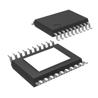
8-Pin SOIC and 20-Pin TSSOP PowerPAD
(PWP) Package
Thermal Shutdown Protection
PWP PACKAGE
(TOP VIEW)
GND/HSINK
GND/HSINK
GND
NC
EN
IN
IN
NC
GND/HSINK
GND/HSINK
1
2
3
4
5
6
7
8
9
10
D PACKAGE
(TOP VIEW)
GND
EN
IN
IN
TPS777xx and TPS778xx are designed to have a
fast transient response and be stable with a 10 µF
low ESR capacitor. This combination provides
high performance at a reasonable cost.
TPS77x33
DROPOUT VOLTAGE
vs
FREE-AIR TEMPERATURE
IO = 10 mA
100
10−1
IO = 0
Co = 10 µF
10−2
−60 −40 −20
0
20
40
60
∆ VO − Change in
Output Voltage − mV
I O − Output Current − mA
VDO − Dropout Voltage − mV
101
80 100 120 140
TA − Free-Air Temperature − °C
1
8
2
7
3
6
4
5
RESET/PG
FB/NC
OUT
OUT
TPS77x33
LOAD TRANSIENT RESPONSE
103
IO = 750 mA
GND/HSINK
GND/HSINK
NC
NC
RESET/PG
FB/NC
OUT
OUT
GND/HSINK
GND/HSINK
NC − No internal connection
description
102
20
19
18
17
16
15
14
13
12
11
Co = 2x47 µF
ESR = 1/2x100 mΩ
VO = 3.3 V
VI = 4.3 V
50
0
−50
1000
500
0
0
20
40
60
80 100 120 140 160 180 200
t − Time − µs
Please be aware that an important notice concerning availability, standard warranty, and use in critical applications of Texas Instruments
semiconductor products and disclaimers thereto appears at the end of this data sheet.
All trademarks are the property of their respective owners.
���������� ����
�!"#�$�
"�
% &'##(�� $% "! )'*+
&$�
"� ,$�(- �#",'&�%
&"�!"#� �" %)(&
!
&$�
"�% )(# ��( �(#�% "! �(.$% ��%�#'�(��% %�$�,$#, �$##$��/�#",'&�
"� )#"&(%%
�0 ,"(% �"� �(&(%%$#
+/
�&+',( �(%�
�0 "! $++ )$#$�(�(#%-
Copyright 1999 − 2004, Texas Instruments Incorporated1
���������� ��������� ������� � ������
�� �������� �
�� ����� ������
����� ��� ����� ��� ����� � � �����
�� ����� �� �
�� �� ������
����������������������� ������ ����������� ������ ����������
www.ti.com
SLVS230G − SEPTEMBER 1999 − REVISED JANUARY 2004
description (continued)
Because the PMOS device behaves as a low-value resistor, the dropout voltage is very low (typically 260 mV at an output
current of 750 mA for the TPS77x33) and is directly proportional to the output current. Additionally, since the PMOS pass
element is a voltage-driven device, the quiescent current is very low and independent of output loading (typically 85 µA over
the full range of output current, 0 mA to 750 mA). These two key specifications yield a significant improvement in operating
life for battery-powered systems. This LDO family also features a sleep mode; applying a TTL high signal to EN (enable)
shuts down the regulator, reducing the quiescent current to 1 µA at TJ = 25°C.
The RESET output of the TPS777xx initiates a reset in microcomputer and microprocessor systems in the event of an
undervoltage condition. An internal comparator in the TPS777xx monitors the output voltage of the regulator to detect an
undervoltage condition on the regulated output voltage.
Power good (PG) of the TPS778xx is an active high output, which can be used to implement a power-on reset or a
low-battery indicator.
The TPS777xx and TPS778xx are offered in 1.5-V, 1.8-V, 2.5-V, and 3.3-V fixed-voltage versions and in an adjustable
version (programmable over the range of 1.5 V to 5.5 V for the TPS77701 option and 1.2 V to 5.5 V for the TPS77801 option).
Output voltage tolerance is specified as a maximum of 2% over line, load, and temperature ranges. The TPS777xx and
TPS778xx families are available in 8-pin SOIC and 20-pin PWP packages.
AVAILABLE OPTIONS
OUTPUT
VOLTAGE
(V)
TJ
PACKAGED DEVICES
TSSOP
(PWP)
TYP
SOIC
(D)
3.3
TPS77733PWP
TPS77833PWP
TPS77733D
TPS77833D
2.5
TPS77725PWP
TPS77825PWP
TPS77725D
TPS77825D
1.8
TPS77718PWP
TPS77818PWP
TPS77718D
TPS77818D
1.5
TPS77715PWP
TPS77815PWP
TPS77715D
TPS77815D
Adjustable
1.5 V to 5.5 V
TPS77701PWP
—
TPS77701D
—
Adjustable
1.2 V to 5.5 V
—
TPS77801PWP
—
TPS77801D
−40°C to 125°C
The TPS77x01 is programmable using an external resistor divider (see application information). The D and PWP
packages are available taped and reeled. Add an R suffix to the device type (e.g., TPS77701DR).
VI
6
RESET/
PG
IN
7
16
RESET/PG
IN
OUT
0.1 µF
5
EN
OUT
14
VO
13
+
GND
Co(1)
10 µF
3
(1) See application information section for capacitor selection details.
Figure 1. Typical Application Configuration for Fixed Output Options
2
�www.ti.com
��������� ��������� ������� � ������
�� �������� �
�� ����� ������
����� ��� ����� ��� ����� � � �����
�� ����� �� �
�� �� ������
����������������������� ������ ����������� ������ ����������
SLVS230G − SEPTEMBER 1999 − REVISED JANUARY 2004
functional block diagram—adjustable version
IN
EN
PG or RESET
_
+
OUT
+
_
200 ms Delay
(for RESET Option)
Vref = 1.1834 V
R1
FB/NC
R2
GND
External to the device
functional block diagram—fixed-voltage version
IN
EN
PG or RESET
_
+
OUT
+
_
200 ms Delay
(for RESET Option)
R1
Vref = 1.1834 V
R2
GND
3
���������� ��������� ������� � ������
�� �������� �
�� ����� ������
����� ��� ����� ��� ����� � � �����
�� ����� �� �
�� �� ������
����������������������� ������ ����������� ������ ����������
SLVS230G − SEPTEMBER 1999 − REVISED JANUARY 2004
Terminal Functions
SOIC Package (TPS777xx)
TERMINAL
NAME
I/O
NO.
DESCRIPTION
EN
2
I
Enable input
FB/NC
7
I
Feedback input voltage for adjustable device (no connect for fixed options)
GND
1
Regulator ground
IN
3, 4
I
Input voltage
OUT
5, 6
O
Regulated output voltage
8
O
RESET output
RESET
TSSOP Package (TPS777xx)
TERMINAL
NAME
I/O
NO.
DESCRIPTION
EN
5
I
Enable input
FB/NC
15
I
Feedback input voltage for adjustable device (no connect for fixed options)
GND
GND/HSINK
3
Regulator ground
1, 2, 9, 10, 11,
12, 19, 20
Ground/heatsink
IN
6, 7
NC
4, 8, 17, 18
OUT
I
Input
No connect
13, 14
O
Regulated output voltage
16
O
RESET output
RESET
SOIC Package (TPS778xx)
TERMINAL
NAME
I/O
NO.
DESCRIPTION
EN
2
I
Enable input
FB/NC
7
I
Feedback input voltage for adjustable device (no connect for fixed options)
GND
1
Regulator ground
IN
3, 4
I
Input voltage
OUT
5, 6
O
Regulated output voltage
8
O
PG output
PG
TSSOP Package (TPS778xx)
TERMINAL
NAME
NO.
I/O
DESCRIPTION
EN
5
I
Enable input
FB/NC
15
I
Feedback input voltage for adjustable device (no connect for fixed options)
GND
3
Regulator ground
1, 2, 9, 10, 11,
12, 19, 20
Ground/heatsink
GND/HSINK
IN
6, 7
NC
4, 8, 17, 18
OUT
PG
4
I
Input
No connect
13, 14
O
Regulated output voltage
16
O
PG output
www.ti.com
�www.ti.com
��������� ��������� ������� � ������
�� �������� �
�� ����� ������
����� ��� ����� ��� ����� � � �����
�� ����� �� �
�� �� ������
����������������������� ������ ����������� ������ ����������
SLVS230G − SEPTEMBER 1999 − REVISED JANUARY 2004
TPS777xx RESET timing diagram
VI
Vres(1)
Vres
t
VO
VIT +(2)
VIT+(2)
Threshold
Voltage
VIT−(2)
Less than 5% of the
output voltage
VIT−(2)
t
RESET
Output
ÎÎ
ÎÎ
ÎÎ
ÎÎ
ÎÎ
Output
Undefined
200 ms
Delay
200 ms
Delay
ÎÎ
ÎÎ
ÎÎ
ÎÎ
ÎÎ
Output
Undefined
t
(1) Vres is the minimum input voltage for a valid RESET. The symbol Vres is not currently listed within EIA or JEDEC standards for semiconductor
symbology.
(2) VIT −Trip voltage is typically 5% lower than the output voltage (95%VO) VIT− to VIT+ is the hysteresis voltage.
5
���������� ��������� ������� � ������
�� �������� �
�� ����� ������
����� ��� ����� ��� ����� � � �����
�� ����� �� �
�� �� ������
����������������������� ������ ����������� ������ ����������
www.ti.com
SLVS230G − SEPTEMBER 1999 − REVISED JANUARY 2004
absolute maximum ratings over operating free-air temperature range (unless otherwise noted)(1)
Input voltage range(2), VI . . . . . . . . . . . . . . . . . . . . . . . . . . . . . . . . . . . . . . . . . . . . . . . . . . . . . . . . . . −0.3 V to 13.5 V
Voltage range at EN . . . . . . . . . . . . . . . . . . . . . . . . . . . . . . . . . . . . . . . . . . . . . . . . . . . . . . . . . . . . . . −0.3 V to 16.5 V
Maximum RESET voltage (TPS777xx) . . . . . . . . . . . . . . . . . . . . . . . . . . . . . . . . . . . . . . . . . . . . . . . . . . . . . . 16.5 V
Maximum PG voltage (TPS778xx) . . . . . . . . . . . . . . . . . . . . . . . . . . . . . . . . . . . . . . . . . . . . . . . . . . . . . . . . . 16.5 V
Peak output current . . . . . . . . . . . . . . . . . . . . . . . . . . . . . . . . . . . . . . . . . . . . . . . . . . . . . . . . . . . . . Internally limited
Output voltage, VO (OUT, FB) . . . . . . . . . . . . . . . . . . . . . . . . . . . . . . . . . . . . . . . . . . . . . . . . . . . . . . . . . . . . . . . . 7 V
Continuous total power dissipation . . . . . . . . . . . . . . . . . . . . . . . . . . . . . . . . . . . . . . See dissipation rating tables
Operating junction temperature range, TJ . . . . . . . . . . . . . . . . . . . . . . . . . . . . . . . . . . . . . . . . . . . −40°C to 125°C
Storage temperature range, Tstg . . . . . . . . . . . . . . . . . . . . . . . . . . . . . . . . . . . . . . . . . . . . . . . . . . . −65°C to 150°C
ESD rating, HBM . . . . . . . . . . . . . . . . . . . . . . . . . . . . . . . . . . . . . . . . . . . . . . . . . . . . . . . . . . . . . . . . . . . . . . . . . . 2 kV
(1) Stresses beyond those listed under absolute maximum ratings may cause permanent damage to the device. These are stress ratings only, and
functional operation of the device at these or any other conditions beyond those indicated under recommended operating conditions is not
implied. Exposure to absolute-maximum-rated conditions for extended periods may affect device reliability.
(2) All voltage values are with respect to network terminal ground.
DISSIPATION RATING TABLE 1 − FREE-AIR TEMPERATURES
PACKAGE
D
AIR FLOW
(CFM)
TA < 25°C
POWER RATING
DERATING FACTOR
ABOVE TA = 25°C
TA = 70°C
POWER RATING
TA = 85°C
POWER RATING
0
568 mW
5.68 mW/°C
312 mW
227 mW
250
904 mW
9.04 mW/°C
497 mW
361 mW
DISSIPATION RATING TABLE 2 − FREE-AIR TEMPERATURES
PACKAGE
PWP§
PWP¶
AIR FLOW
(CFM)
TA < 25°C
POWER RATING
DERATING FACTOR
ABOVE TA = 25°C
TA = 70°C
POWER RATING
TA = 85°C
POWER RATING
0
2.9 W
23.5 mW/°C
1.9 W
1.5 W
300
4.3 W
34.6 mW/°C
2.8 W
2.2 W
0
3W
23.8 mW/°C
1.9 W
1.5 W
300
7.2 W
57.9 mW/°C
4.6 W
3.8 W
(1) This parameter is measured with the recommended copper heat sink pattern on a 1-layer PCB, 5 in × 5 in PCB, 1 oz.
copper, 2 in × 2 in coverage (4 in2).
(2) This parameter is measured with the recommended copper heat sink pattern on a 8-layer PCB, 1.5 in × 2 in PCB, 1 oz.
copper with layers 1, 2, 4, 5, 7, and 8 at 5% coverage (0.9 in2) and layers 3 and 6 at 100% coverage (6 in2). For more
information, refer to TI technical brief SLMA002.
recommended operating conditions
MIN
MAX
2.7
10
TPS77701
1.5
5.5
TPS77801
1.2
5.5
−40
125
Input voltage, VI(1)
Output voltage range, VO
Operating junction temperature, TJ
(1) Minimum VIN = VOUT + VDO or 2.7V, whichever is greater.
6
UNIT
V
V
°C
�www.ti.com
��������� ��������� ������� � ������
�� �������� �
�� ����� ������
����� ��� ����� ��� ����� � � �����
�� ����� �� �
�� �� ������
����������������������� ������ ����������� ������ ����������
SLVS230G − SEPTEMBER 1999 − REVISED JANUARY 2004
electrical characteristics over recommended operating temperature range (TJ = −40°C to 125°C),
VI = VO(typ) + 1 V, IO = 1 mA, EN = 0 V, Co = 10 µF (unless otherwise noted)
PARAMETER
TEST CONDITIONS
TPS77701
TPS77801
1.5 V ≤ VO ≤ 5.5 V,
TJ = 25°C
1.5 V ≤ VO ≤ 5.5 V,
1.2 V ≤ VO ≤ 5.5 V,
TPS77x18
TPS77x25
TJ = 25°C,
TJ = −40°C to 125°C,
3.5 V < VIN < 10 V
TPS77x33
TJ = 25°C,
TJ = −40°C to 125°C,
4.3 V < VIN < 10 V
Output voltage line regulation (∆VO/VO)
VO
2.7 V < VIN < 10 V
1.470
2.8 V < VIN < 10 V
1.764
4.3 V < VIN < 10 V
10 µA < IO < 750 mA, TJ = 25°C
IO = 750 mA
Output current limit
VO = 0 V
2.5
Standby current
2.550
3.3
3.234
3.366
85
125
1.2
Thermal shutdown junction temperature
EN = VI,
TJ = 25°C,
2.7 V < VI < 10 V
%/V
3
mV
54
µVrms
1.7
1
µA
2
V
Reset
(TPS777xx)
0.9
Minimum input voltage for valid RESET
Trip threshold voltage
VO decreasing
Hysteresis voltage
Measured at VO
Output low voltage
VI = 2.7 V,
Leakage current
V(RESET) = 5 V
RESET time-out delay
Co = 10 µF,
60
V
98
0.5
0.15
200
V
dB
1.1
92
IO(RESET) = 1 mA
µA
nA
1.7
Low level enable input voltage
f = 1 KHz,
TJ = 25°C
IO(RESET) = 300 µA
A
°C
10
FB = 1.5 V
High level enable input voltage
Power supply ripple rejection
2
150
EN = VI,
TPS77x01
µA
A
0.01
2.7 V < VI < 10 V
FB input current
V
1.836
2.450
VO + 1 V < VI ≤ 10 V, TJ = 25°C
BW = 200 Hz to 100 kHz, Co = 10 µF,
TJ = 25°C, IC = 750 µA
1.530
1.8
Load regulation
Output noise voltage (TPS77x18)
1.02VO
1.5
2.7 V < VIN < 10 V
2.8 V < VIN < 10 V
3.5 V < VIN < 10 V
UNIT
1.02VO
0.98VO
TJ = 25°C,
TJ = −40°C to 125°C,
MAX
VO
TJ = 25°C
1.2 V ≤ VO ≤ 5.5 V,
TPS77x15
Quiescent current (GND current)
TYP
0.98VO
TJ = 25°C,
TJ = −40°C to 125°C,
Output voltage (10 µA
A to 750 mA load)
MIN
%VO
%VO
0.4
V
1
µA
ms
7
���������� ��������� ������� � ������
�� �������� �
�� ����� ������
����� ��� ����� ��� ����� � � �����
�� ����� �� �
�� �� ������
����������������������� ������ ����������� ������ ����������
www.ti.com
SLVS230G − SEPTEMBER 1999 − REVISED JANUARY 2004
electrical characteristics over recommended operating temperature range (TJ = −40°C to 125°C),
VI = VO(typ) + 1 V, IO = 1 mA, EN = 0 V, Co = 10 µF (unless otherwise noted) (continued)
PARAMETER
TEST CONDITIONS
Minimum input voltage for valid PG
Trip threshold voltage
PG
Hysteresis voltage
(TPS778xx)
Output low voltage
IO(PG) = 300 µA
VO decreasing
MIN
Leakage current
Input current (EN)
92
UNIT
V
98
%VO
%VO
0.4
V
1
µA
0.5
IO(PG) = 1 mA
0.15
EN = 0 V
−1
EN = VI
−1
TPS77733
IO = 750 mA,
IO = 750 mA,
TJ = 25°C
TPS77833
IO = 750 mA,
IO = 750 mA,
TJ = 25°C
Dropout voltage (1)
MAX
1.1
Measured at VO
VI = 2.7 V,
V(PG) = 5 V
TYP
0
1
A
µA
1
260
427
mV
260
427
(1) IN voltage equals VO(typ) − 100 mV; TPS77x01 output voltage set to 3.3 V nominal with external resistor divider. TPS77x15, TPS77x18, and
TPS77x25 dropout voltage limited by input voltage range limitations (i.e., TPS77x33 input voltage needs to drop to 3.2 V for purpose of this
test).
TYPICAL CHARACTERISTICS
Table of Graphs
FIGURE
VO
Output voltage
2, 3, 4
vs Free-air temperature
5, 6, 7
Ground current
vs Free-air temperature
8
Power supply ripple rejection
vs Frequency
9
Output spectral noise density
vs Frequency
10
Zo
Output impedance
vs Frequency
11
VDO
Dropout voltage
Input voltage (min)
VO
8
vs Output current
vs Input voltage
12
vs Free-air temperature
13
vs Output voltage
14
Line transient response
15, 17
Load transient response
16, 18
Output voltage
vs Time
Equivalent series resistance (ESR)
vs Output current
19
21 − 24
�www.ti.com
��������� ��������� ������� � ������
�� �������� �
�� ����� ������
����� ��� ����� ��� ����� � � �����
�� ����� �� �
�� �� ������
����������������������� ������ ����������� ������ ����������
SLVS230G − SEPTEMBER 1999 − REVISED JANUARY 2004
TYPICAL CHARACTERISTICS
TPS77x33
TPS77x15
OUTPUT VOLTAGE
vs
OUTPUT CURRENT
OUTPUT VOLTAGE
vs
OUTPUT CURRENT
1.4985
3.2835
VI = 4.3 V
TA = 25°C
3.2830
VI = 2.7 V
TA = 25°C
1.4980
1.4975
VO − Output Voltage − V
VO − Output Voltage − V
3.2825
1.4970
3.2820
1.4965
3.2815
1.4960
3.2810
1.4955
3.2805
1.4950
3.2800
0.125
0
0.25 0.375
0.5
IO − Output Current − A
0.675
0
0.75
0.125
0.25
0.375
0.5
0.675
0.75
IO − Output Current − A
Figure 2
Figure 3
TPS77x25
TPS77x33
OUTPUT VOLTAGE
vs
OUTPUT CURRENT
OUTPUT VOLTAGE
vs
FREE-AIR TEMPERATURE
2.4960
3.32
VI = 4.3 V
VI = 3.5 V
TA = 25°C
2.4955
3.31
VO − Output Voltage − V
VO − Output Voltage − V
2.4950
2.4945
2.4940
2.4935
2.4930
3.30
3.29
IO = 750 mA
IO = 1 mA
3.28
3.27
3.26
2.4925
2.4920
0
0.125
0.25
0.375
0.5
IO − Output Current − A
Figure 4
0.675
0.75
3.25
−60 −40 −20
0
20
40
60
80
100 120 140
TA − Free-Air Temperature − °C
Figure 5
9
���������� ��������� ������� � ������
�� �������� �
�� ����� ������
����� ��� ����� ��� ����� � � �����
�� ����� �� �
�� �� ������
����������������������� ������ ����������� ������ ����������
www.ti.com
SLVS230G − SEPTEMBER 1999 − REVISED JANUARY 2004
TYPICAL CHARACTERISTICS
TPS77x15
TPS77x25
OUTPUT VOLTAGE
vs
FREE-AIR TEMPERATURE
OUTPUT VOLTAGE
vs
FREE-AIR TEMPERATURE
1.515
2.515
VI = 3.5 V
VI = 2.7 V
2.510
VO − Output Voltage − V
VO − Output Voltage − V
1.510
1.505
1.500
IO = 750 mA
IO = 1 mA
1.495
1.490
2.505
2.500
IO = 750 mA
2.495
IO = 1 mA
2.490
2.485
1.485
−60 −40 −20
0
20
40
60
80
2.480
−60 −40
100 120 140
TA − Free-Air Temperature − °C
−20
Figure 6
TPS77xxx
60
80
100 120
TPS77x33
IO = 500 mA
IO = 1 mA
85
IO = 750 mA
80
75
−60 −40 −20
0
20
40
60
80
100 120 140
TA − Free-Air Temperature − °C
Figure 8
PSRR − Power Supply Ripple Rejection − dB
90
95
Ground Current − µ A
40
POWER SUPPLY RIPPLE REJECTION
vs
FREQUENCY
100
10
20
Figure 7
GROUND CURRENT
vs
FREE-AIR TEMPERATURE
90
0
TA − Free-Air Temperature − °C
VI = 4.3 V
Co = 10 µF
TA = 25°C
80
70
60
50
40
30
20
10
0
−10
10
100
1k
10k
f − Frequency − Hz
Figure 9
100k
1M
�www.ti.com
��������� ��������� ������� � ������
�� �������� �
�� ����� ������
����� ��� ����� ��� ����� � � �����
�� ����� �� �
�� �� ������
����������������������� ������ ����������� ������ ����������
SLVS230G − SEPTEMBER 1999 − REVISED JANUARY 2004
TYPICAL CHARACTERISTICS
TPS77x33
TPS77x33
OUTPUT SPECTRAL NOISE DENSITY
vs
FREQUENCY
OUTPUT IMPEDANCE
vs
FREQUENCY
0
VI = 4.3 V
Co = 10 µF
TA = 25°C
VI = 4.3 V
Co = 10 µF
TA = 25°C
Zo − Output Impedance − Ω
Output Spectral Noise Density − µV Hz
10−5
IO = 7 mA
10−6
IO = 750 mA
10−7
10−8
102
103
104
IO = 1 mA
10−1
IO = 750 mA
10−2
101
105
102
103
104
f − Frequency − kHz
f − Frequency − Hz
Figure 10
105
106
Figure 11
TPS77x33
DROPOUT VOLTAGE
vs
FREE-AIR TEMPERATURE
TPS77x01
DROPOUT VOLTAGE
vs
INPUT VOLTAGE
103
600
IO = 750 mA
VDO − Dropout Voltage − mV
VDO − Dropout Voltage − mV
500
400
TA = 125°C
TA = 25°C
300
200
TA = −40°C
100
102
IO = 750 mA
101
IO = 10 mA
100
10−1
IO = 0
Co = 10 µF
0
2.5
3
3.5
4
VI − Input Voltage − V
Figure 12
4.5
5
10−2
−60 −40 −20
0
20
40
60
80 100 120 140
TA − Free-Air Temperature − °C
Figure 13
11
���������� ��������� ������� � ������
�� �������� �
�� ����� ������
����� ��� ����� ��� ����� � � �����
�� ����� �� �
�� �� ������
����������������������� ������ ����������� ������ ����������
www.ti.com
SLVS230G − SEPTEMBER 1999 − REVISED JANUARY 2004
TYPICAL CHARACTERISTICS
INPUT VOLTAGE (MIN)
vs
OUTPUT VOLTAGE
TPS77x15
LINE TRANSIENT RESPONSE
VI − Input Voltage − V
4
TA = 25°C
TA = 125°C
3.7
2.7
3
TA = −40°C
∆ VO − Change in
Output Voltage − mV
VI − Input Voltage (Min) − V
IO = 0.75 A
2.7
2
1.5
1.75
2
2.25
2.5
2.75
3
3.25
3.5
10
0
−10
Co = 10 µF
TA = 25°C
0
VO − Output Voltage − V
20
40
60
TPS77x33
LINE TRANSIENT RESPONSE
0
−50
Co = 10 µF
TA = 25°C
5.3
4.3
1000
500
0
0
20
40
60
80 100 120 140 160 180 200
t − Time − µs
Figure 16
12
VI − Input Voltage − V
TPS77x15
LOAD TRANSIENT RESPONSE
Co = 2x47 µF
ESR = 1/2x100 mΩ
VO = 1.5 V
VI = 2.7 V
50
Figure 15
∆ VO − Change in
Output Voltage − mV
I O − Output Current − mA
∆ VO − Change in
Output Voltage − mV
Figure 14
80 100 120 140 160 180 200
t − Time − µs
10
0
−10
0
20
40
60
80 100 120 140 160 180 200
t − Time − µs
Figure 17
�www.ti.com
��������� ��������� ������� � ������
�� �������� �
�� ����� ������
����� ��� ����� ��� ����� � � �����
�� ����� �� �
�� �� ������
����������������������� ������ ����������� ������ ����������
SLVS230G − SEPTEMBER 1999 − REVISED JANUARY 2004
TYPICAL CHARACTERISTICS
TPS77x33
OUTPUT VOLTAGE
vs
TIME (AT STARTUP)
TPS77x33
4
50
0
VO− Output Voltage − V
Co = 2x47 µF
ESR = 1/2x100 mΩ
VO = 3.3 V
VI = 4.3 V
−50
1000
Co = 10 µF
IO = 750 mA
TA = 25°C
3
2
1
0
500
Enable Pulse − V
I O − Output Current − mA
∆ VO − Change in
Output Voltage − mV
LOAD TRANSIENT RESPONSE
0
20
0
40
60
80 100 120 140 160 180 200
t − Time − µs
0
0
0.1
Figure 18
VI
0.2 0.3
0.4 0.5 0.6 0.7 0.8
t − Time − ms
0.9
1
Figure 19
To Load
IN
OUT
+
EN
Co
GND
R
RL
ESR
Figure 20. Test Circuit for Typical Regions of Stability (Figures 21 through 24) (Fixed Output Options)
13
���������� ��������� ������� � ������
�� �������� �
�� ����� ������
����� ��� ����� ��� ����� � � �����
�� ����� �� �
�� �� ������
����������������������� ������ ����������� ������ ����������
www.ti.com
SLVS230G − SEPTEMBER 1999 − REVISED JANUARY 2004
TYPICAL CHARACTERISTICS
TYPICAL REGION OF STABILITY
TYPICAL REGION OF STABILITY
EQUIVALENT SERIES RESISTANCE(1)
vs
OUTPUT CURRENT
EQUIVALENT SERIES RESISTANCE(1)
vs
OUTPUT CURRENT
10
ESR − Equivalent Series Resistance − Ω
ESR − Equivalent Series Resistance − Ω
10
Region of Instability
1
VO = 3.3 V
Co = 4.7 µF
VI = 4.3 V
TA = 25°C
Region of Stability
0.1
Region of Instability
1
VO = 3.3 V
Co = 4.7 µF
VI = 4.3 V
TJ = 125°C
0.1
Region of Instability
Region of Instability
0.01
0.01
0
125
250
375
500
625
0
750
125
250
375
500
625
750
IO − Output Current − mA
IO − Output Current − mA
Figure 21
Figure 22
TYPICAL REGION OF STABILITY
TYPICAL REGION OF STABILITY
EQUIVALENT SERIES RESISTANCE(1)
vs
OUTPUT CURRENT
EQUIVALENT SERIES RESISTANCE(1)
vs
OUTPUT CURRENT
10
10
Region of Instability
ESR − Equivalent Series Resistance − Ω
ESR − Equivalent Series Resistance − Ω
Region of Stability
1
VO = 3.3 V
Co = 22 µF
VI = 4.3 V
TA = 25°C
Region of Stability
0.1
Region of Instability
Region of Instability
1
VO = 3.3 V
Co = 22 µF
VI = 4.3 V
TJ = 125°C
Region of Stability
0.1
Region of Instability
0.01
0.01
0
125
250
375
500
IO − Output Current − mA
Figure 23
625
750
0
125
250
375
500
625
750
IO − Output Current − mA
Figure 24
(1) Equivalent series resistance (ESR) refers to the total series resistance, including the ESR of the capacitor, any series resistance added
externally, and PWB trace resistance to Co.
14
�www.ti.com
��������� ��������� ������� � ������
�� �������� �
�� ����� ������
����� ��� ����� ��� ����� � � �����
�� ����� �� �
�� �� ������
����������������������� ������ ����������� ������ ����������
SLVS230G − SEPTEMBER 1999 − REVISED JANUARY 2004
APPLICATION INFORMATION
The TPS777xx and TPS778xx families include four fixed-output voltage regulators (1.5 V, 1.8 V, 2.5 V, and 3.3 V), and an
adjustable regulator, the TPS77x01 (adjustable from 1.5 V to 5.5 V for TPS77701 option and 1.2 V to 5.5 V for TPS77801
option).
device operation
The TPS777xx and TPS778xx feature very low quiescent current, which remains virtually constant even with varying loads.
Conventional LDO regulators use a pnp pass element, the base current of which is directly proportional to the load current
through the regulator (IB = IC/β). The TPS777xx and TPS778xx use a PMOS transistor to pass current; because the gate
of the PMOS is voltage driven, operating current is low and invariable over the full load range.
Another pitfall associated with the pnp-pass element is its tendency to saturate when the device goes into dropout. The
resulting drop in β forces an increase in IB to maintain the load. During power up, this translates to large start-up currents.
Systems with limited supply current may fail to start up. In battery-powered systems, it means rapid battery discharge when
the voltage decays below the minimum required for regulation. The TPS777xx and TPS778xx quiescent currents remain
low even when the regulator drops out, eliminating both problems.
The TPS777xx and TPS778xx families also feature a shutdown mode that places the output in the high-impedance state
(essentially equal to the feedback-divider resistance) and reduces quiescent current to 2 µA. If the shutdown feature is not
used, EN should be tied to ground.
minimum load requirements
The TPS777xx and TPS778xx families are stable even at zero load; no minimum load is required for operation.
FB—pin connection (adjustable version only)
The FB pin is an input pin to sense the output voltage and close the loop for the adjustable option . The output voltage is
sensed through a resistor divider network to close the loop as it is shown in Figure 26. Normally, this connection should
be as short as possible; however, the connection can be made near a critical circuit to improve performance at that point.
Internally, FB connects to a high-impedance wide-bandwidth amplifier and noise pickup feeds through to the regulator
output. Routing the FB connection to minimize/avoid noise pickup is essential.
external capacitor requirements
An input capacitor is not usually required; however, a ceramic bypass capacitor (0.047 µF or larger) improves load transient
response and noise rejection if the TPS777xx or TPS778xx are located more than a few inches from the power supply. A
higher-capacitance electrolytic capacitor may be necessary if large (hundreds of milliamps) load transients with fast rise
times are anticipated.
Like all low dropout regulators, the TPS777xx and TPS778xx require an output capacitor connected between OUT and
GND to stabilize the internal control loop. The minimum recommended capacitance value is 10 µF and the ESR (equivalent
series resistance) must be between 50 mΩ and 1.5 Ω. Capacitor values 10 µF or larger are acceptable, provided the ESR
is less than 1.5 Ω. Solid tantalum electrolytic, aluminum electrolytic, and multilayer ceramic capacitors are all suitable,
provided they meet the requirements described previously.
15
���������� ��������� ������� � ������
�� �������� �
�� ����� ������
����� ��� ����� ��� ����� � � �����
�� ����� �� �
�� �� ������
����������������������� ������ ����������� ������ ����������
www.ti.com
SLVS230G − SEPTEMBER 1999 − REVISED JANUARY 2004
APPLICATION INFORMATION
external capacitor requirements (continued)
6
VI
16
IN RESET/
PG
IN
14
OUT
13
EN
OUT
7
C1
0.1 µF
5
GND
RESET/PG
250 kΩ
VO
+
Co
10 µF
3
Figure 25. Typical Application Circuit (Fixed Versions)
programming the TPS77x01 adjustable LDO regulator
The output voltage of the TPS77x01 adjustable regulator is programmed using an external resistor divider as shown in
Figure 26. The output voltage is calculated using:
V
O
+V
ǒ1 ) R1
Ǔ
R2
ref
(1)
Where:
Vref = 1.1834 V typ (the internal reference voltage)
Resistors R1 and R2 should be chosen for approximately 10-µA divider current. Lower value resistors can be used but offer
no inherent advantage and waste more power. Higher values should be avoided as leakage currents at FB increase the
output voltage error. The recommended design procedure is to choose R2 = 110 kΩ to set the divider current at
approximately 10 µA and then calculate R1 using:
R1 +
ǒ
V
V
Ǔ
O *1
ref
R2
(2)
OUTPUT VOLTAGE
PROGRAMMING GUIDE
TPS77x01
VI
0.1 µF
IN
RESET/
PG
250 kΩ
≥ 1.7 V
≤ 0.9 V
Reset or PG Output
EN
OUT
VO
R1
FB / NC
GND
Co
OUTPUT
VOLTAGE
R1
UNIT
2.5 V
121
110
kΩ
3.3 V
196
110
kΩ
3.6 V
226
110
kΩ
4.75 V
332
110
kΩ
R2
Figure 26. TPS77x01 Adjustable LDO Regulator Programming
16
R2
�www.ti.com
��������� ��������� ������� � ������
�� �������� �
�� ����� ������
����� ��� ����� ��� ����� � � �����
�� ����� �� �
�� �� ������
����������������������� ������ ����������� ������ ����������
SLVS230G − SEPTEMBER 1999 − REVISED JANUARY 2004
APPLICATION INFORMATION
reset indicator
The TPS777xx features a RESET output that can be used to monitor the status of the regulator. The internal comparator
monitors the output voltage: when the output drops to between 92% and 98% of its nominal regulated value, the RESET
output transistor turns on, taking the signal low. The open-drain output requires a pullup resistor. If not used, it can be left
floating. RESET can be used to drive power-on reset circuitry or as a low-battery indicator. RESET does not assert itself
when the regulated output voltage falls outside the specified 2% tolerance, but instead reports an output voltage low relative
to its nominal regulated value (refer to timing diagram for start-up sequence).
power-good indicator
The TPS778xx features a power-good (PG) output that can be used to monitor the status of the regulator. The internal
comparator monitors the output voltage: when the output drops to between 92% and 98% of its nominal regulated value,
the PG output transistor turns on, taking the signal low. The open-drain output requires a pullup resistor. If not used, it can
be left floating. PG can be used to drive power-on reset circuitry or used as a low-battery indicator.
regulator protection
The TPS777xx and TPS778xx PMOS-pass transistors have a built-in back diode that conducts reverse currents when the
input voltage drops below the output voltage (e.g., during power down). Current is conducted from the output to the input
and is not internally limited. When extended reverse voltage is anticipated, external limiting may be appropriate.
The TPS777xx and TPS778xx also feature internal current limiting and thermal protection. During normal operation, the
TPS777xx and TPS778xx limit output current to approximately 1.7 A. When current limiting engages, the output voltage
scales back linearly until the overcurrent condition ends. While current limiting is designed to prevent gross device failure,
care should be taken not to exceed the power dissipation ratings of the package. If the temperature of the device exceeds
150°C(typ), thermal-protection circuitry shuts it down. Once the device has cooled below 130°C(typ), regulator operation
resumes.
17
���������� ��������� ������� � ������
�� �������� �
�� ����� ������
����� ��� ����� ��� ����� � � �����
�� ����� �� �
�� �� ������
����������������������� ������ ����������� ������ ����������
www.ti.com
SLVS230G − SEPTEMBER 1999 − REVISED JANUARY 2004
APPLICATION INFORMATION
POWER DISSIPATION AND JUNCTION TEMPERATURE
Specified regulator operation is assured to a junction temperature of 125°C; the maximum junction temperature should be
restricted to 125°C under normal operating conditions. This restriction limits the power dissipation the regulator can handle
in any given application. To ensure the junction temperature is within acceptable limits, calculate the maximum allowable
dissipation, PD(max), and the actual dissipation, PD, which must be less than or equal to PD(max).
The maximum-power-dissipation limit is determined using the following equation:
P
T max * T
A
+ J
D(max)
R
qJA
Where:
TJmax is the maximum allowable junction temperature.
RθJA is the thermal resistance junction-to-ambient for the package, and is calculated as
1
derating factor
from the dissipation rating tables.
TA is the ambient temperature.
The regulator dissipation is calculated using:
P
D
ǒ
Ǔ
+ V *V
I
O
I
O
Power dissipation resulting from quiescent current is negligible. Excessive power dissipation will trigger the thermal
protection circuit.
18
�PACKAGE OPTION ADDENDUM
www.ti.com
14-Oct-2022
PACKAGING INFORMATION
Orderable Device
Status
(1)
Package Type Package Pins Package
Drawing
Qty
Eco Plan
(2)
Lead finish/
Ball material
MSL Peak Temp
Op Temp (°C)
Device Marking
(3)
Samples
(4/5)
(6)
TPS77701D
ACTIVE
SOIC
D
8
75
RoHS & Green
NIPDAU
Level-1-260C-UNLIM
-40 to 125
77701
Samples
TPS77701DR
ACTIVE
SOIC
D
8
2500
RoHS & Green
NIPDAU
Level-1-260C-UNLIM
-40 to 125
77701
Samples
TPS77701PWP
ACTIVE
HTSSOP
PWP
20
70
RoHS & Green
NIPDAU
Level-2-260C-1 YEAR
-40 to 125
PT77701
Samples
TPS77701PWPR
ACTIVE
HTSSOP
PWP
20
2000
RoHS & Green
NIPDAU
Level-2-260C-1 YEAR
-40 to 125
PT77701
Samples
TPS77715D
ACTIVE
SOIC
D
8
75
RoHS & Green
NIPDAU
Level-1-260C-UNLIM
-40 to 125
77715
Samples
TPS77715DR
ACTIVE
SOIC
D
8
2500
RoHS & Green
NIPDAU
Level-1-260C-UNLIM
-40 to 125
77715
Samples
TPS77715PWP
ACTIVE
HTSSOP
PWP
20
70
RoHS & Green
NIPDAU
Level-2-260C-1 YEAR
-40 to 125
PT77715
Samples
TPS77715PWPG4
ACTIVE
HTSSOP
PWP
20
70
RoHS & Green
NIPDAU
Level-2-260C-1 YEAR
-40 to 125
PT77715
Samples
TPS77718D
ACTIVE
SOIC
D
8
75
RoHS & Green
NIPDAU
Level-1-260C-UNLIM
-40 to 125
77718
Samples
TPS77718DR
ACTIVE
SOIC
D
8
2500
RoHS & Green
NIPDAU
Level-1-260C-UNLIM
-40 to 125
77718
Samples
TPS77718PWP
ACTIVE
HTSSOP
PWP
20
70
RoHS & Green
NIPDAU
Level-2-260C-1 YEAR
-40 to 125
PT77718
Samples
TPS77718PWPG4
ACTIVE
HTSSOP
PWP
20
70
RoHS & Green
NIPDAU
Level-2-260C-1 YEAR
-40 to 125
PT77718
Samples
TPS77718PWPR
ACTIVE
HTSSOP
PWP
20
2000
RoHS & Green
NIPDAU
Level-2-260C-1 YEAR
-40 to 125
PT77718
Samples
TPS77725D
ACTIVE
SOIC
D
8
75
RoHS & Green
NIPDAU
Level-1-260C-UNLIM
-40 to 125
77725
Samples
TPS77725PWP
ACTIVE
HTSSOP
PWP
20
70
RoHS & Green
NIPDAU
Level-2-260C-1 YEAR
-40 to 125
PT77725
Samples
TPS77725PWPR
ACTIVE
HTSSOP
PWP
20
2000
RoHS & Green
NIPDAU
Level-2-260C-1 YEAR
-40 to 125
PT77725
Samples
TPS77733D
ACTIVE
SOIC
D
8
75
RoHS & Green
NIPDAU
Level-1-260C-UNLIM
-40 to 125
77733
Samples
TPS77733DR
ACTIVE
SOIC
D
8
2500
RoHS & Green
NIPDAU
Level-1-260C-UNLIM
-40 to 125
77733
Samples
TPS77733PWP
ACTIVE
HTSSOP
PWP
20
70
RoHS & Green
NIPDAU
Level-2-260C-1 YEAR
-40 to 125
PT77733
Samples
TPS77733PWPR
ACTIVE
HTSSOP
PWP
20
2000
RoHS & Green
NIPDAU
Level-2-260C-1 YEAR
-40 to 125
PT77733
Samples
Addendum-Page 1
�PACKAGE OPTION ADDENDUM
www.ti.com
14-Oct-2022
Orderable Device
Status
(1)
Package Type Package Pins Package
Drawing
Qty
Eco Plan
(2)
Lead finish/
Ball material
MSL Peak Temp
Op Temp (°C)
Device Marking
(3)
Samples
(4/5)
(6)
TPS77801D
ACTIVE
SOIC
D
8
75
RoHS & Green
NIPDAU
Level-1-260C-UNLIM
-40 to 125
77801
Samples
TPS77801DG4
ACTIVE
SOIC
D
8
75
RoHS & Green
NIPDAU
Level-1-260C-UNLIM
-40 to 125
77801
Samples
TPS77801DR
ACTIVE
SOIC
D
8
2500
RoHS & Green
NIPDAU
Level-1-260C-UNLIM
-40 to 125
77801
Samples
TPS77801PWP
ACTIVE
HTSSOP
PWP
20
70
RoHS & Green
NIPDAU
Level-2-260C-1 YEAR
-40 to 125
PT77801
Samples
TPS77801PWPG4
ACTIVE
HTSSOP
PWP
20
70
RoHS & Green
NIPDAU
Level-2-260C-1 YEAR
-40 to 125
PT77801
Samples
TPS77801PWPR
ACTIVE
HTSSOP
PWP
20
2000
RoHS & Green
NIPDAU
Level-2-260C-1 YEAR
-40 to 125
PT77801
Samples
TPS77801PWPRG4
ACTIVE
HTSSOP
PWP
20
2000
RoHS & Green
NIPDAU
Level-2-260C-1 YEAR
-40 to 125
PT77801
Samples
TPS77815D
ACTIVE
SOIC
D
8
75
RoHS & Green
NIPDAU
Level-1-260C-UNLIM
-40 to 125
77815
Samples
TPS77815DR
ACTIVE
SOIC
D
8
2500
RoHS & Green
NIPDAU
Level-1-260C-UNLIM
-40 to 125
77815
Samples
TPS77815PWP
ACTIVE
HTSSOP
PWP
20
70
RoHS & Green
NIPDAU
Level-2-260C-1 YEAR
-40 to 125
PT77815
Samples
TPS77815PWPG4
ACTIVE
HTSSOP
PWP
20
70
RoHS & Green
NIPDAU
Level-2-260C-1 YEAR
-40 to 125
PT77815
Samples
TPS77815PWPR
ACTIVE
HTSSOP
PWP
20
2000
RoHS & Green
NIPDAU
Level-2-260C-1 YEAR
-40 to 125
PT77815
Samples
TPS77818D
ACTIVE
SOIC
D
8
75
RoHS & Green
NIPDAU
Level-1-260C-UNLIM
-40 to 125
77818
Samples
TPS77818PWP
ACTIVE
HTSSOP
PWP
20
70
RoHS & Green
NIPDAU
Level-2-260C-1 YEAR
-40 to 125
PT77818
Samples
TPS77818PWPG4
ACTIVE
HTSSOP
PWP
20
70
RoHS & Green
NIPDAU
Level-2-260C-1 YEAR
-40 to 125
PT77818
Samples
TPS77818PWPR
ACTIVE
HTSSOP
PWP
20
2000
RoHS & Green
NIPDAU
Level-2-260C-1 YEAR
-40 to 125
PT77818
Samples
TPS77825D
ACTIVE
SOIC
D
8
75
RoHS & Green
NIPDAU
Level-1-260C-UNLIM
-40 to 125
77825
Samples
TPS77825DR
ACTIVE
SOIC
D
8
2500
RoHS & Green
NIPDAU
Level-1-260C-UNLIM
-40 to 125
77825
Samples
TPS77825PWP
ACTIVE
HTSSOP
PWP
20
70
RoHS & Green
NIPDAU
Level-2-260C-1 YEAR
-40 to 125
PT77825
Samples
TPS77825PWPR
ACTIVE
HTSSOP
PWP
20
2000
RoHS & Green
NIPDAU
Level-2-260C-1 YEAR
-40 to 125
PT77825
Samples
TPS77833D
ACTIVE
SOIC
D
8
75
RoHS & Green
NIPDAU
Level-1-260C-UNLIM
-40 to 125
77833
Samples
Addendum-Page 2
�PACKAGE OPTION ADDENDUM
www.ti.com
14-Oct-2022
Orderable Device
Status
(1)
Package Type Package Pins Package
Drawing
Qty
Eco Plan
(2)
Lead finish/
Ball material
MSL Peak Temp
Op Temp (°C)
Device Marking
(3)
Samples
(4/5)
(6)
TPS77833DR
ACTIVE
SOIC
D
8
2500
RoHS & Green
NIPDAU
Level-1-260C-UNLIM
-40 to 125
77833
Samples
TPS77833PWP
ACTIVE
HTSSOP
PWP
20
70
RoHS & Green
NIPDAU
Level-2-260C-1 YEAR
-40 to 125
PT77833
Samples
TPS77833PWPR
ACTIVE
HTSSOP
PWP
20
2000
RoHS & Green
NIPDAU
Level-2-260C-1 YEAR
-40 to 125
PT77833
Samples
(1)
The marketing status values are defined as follows:
ACTIVE: Product device recommended for new designs.
LIFEBUY: TI has announced that the device will be discontinued, and a lifetime-buy period is in effect.
NRND: Not recommended for new designs. Device is in production to support existing customers, but TI does not recommend using this part in a new design.
PREVIEW: Device has been announced but is not in production. Samples may or may not be available.
OBSOLETE: TI has discontinued the production of the device.
(2)
RoHS: TI defines "RoHS" to mean semiconductor products that are compliant with the current EU RoHS requirements for all 10 RoHS substances, including the requirement that RoHS substance
do not exceed 0.1% by weight in homogeneous materials. Where designed to be soldered at high temperatures, "RoHS" products are suitable for use in specified lead-free processes. TI may
reference these types of products as "Pb-Free".
RoHS Exempt: TI defines "RoHS Exempt" to mean products that contain lead but are compliant with EU RoHS pursuant to a specific EU RoHS exemption.
Green: TI defines "Green" to mean the content of Chlorine (Cl) and Bromine (Br) based flame retardants meet JS709B low halogen requirements of


 工商网监
湘ICP备2023018690号
工商网监
湘ICP备2023018690号
