CY7B952
SST™ SONET/SDH Serial Transceiver
Features
• OC-3 Compliant with Bellcore and CCITT (ITU) specifications on: — Jitter Generation ( 0°C VCC − 1.03 VCC − 1.86 0.6 VCC − 0.83 VCC − 1.62 V V V 3.0 VCC − 1.165 2.0 2.5 2.5 −0.5 VCC − 1.475 0.8 REFCLK LOOP REFCLK LOOP VIN=VCC VIN=VCC VIN=0.0V VIN=0.0V IOH=–2 mA IOL=4 mA VOUT=0V[3] VIN=VIHE(MAX) VIN=VIHE(MAX) VIN=VILE(MIN) VIN=VILE(MIN) +0.5 −200 50 100 1200 1200 VCC VCC VCC −15 Test Condition Min. 2.0 −0.5 +0.5 −10 −50 −500 2.4 0.45 −90 +250 +750 Max. VCC 0.8 +200 +10 +50 Unit V V µA µA µA µA V V mA µA µA µA µA mV mV V V V V V V V TTL-compatible Input Pins (LOOP, REFCLK+, REFCLK–)
TTL Compatible Output Pins (LFI)
ECL Compatible Input Pins (REFCLK±, CD, TSER±, RIN±)
Notes: 1. Single Power Supply: The voltage on any input or I/O pin cannot exceed the power pin during power-up. 2. TA is the “instant on” case temperature. 3. Tested one output at a time, output shorted for less than one second, less than 10% duty cycle. 4. Input currents are always positive at all voltages above VCC/2.
Document #: 38-02018 Rev. *B
Page 5 of 9
�CY7B952
Electrical Characteristics Over the Operating Range (continued)
Parameter VIHH VIMM VILL ICCS ICCR ICCT ICCE ICC5 ICCO Description Three-Level Input HIGH Three-Level Input MID Three-Level Input LOW Static Operating Current Receiver Operating Current Transmitter Operating Current ECL Pair Operating Current Additional Current at 51.84 MHz Additional Current LFI=LOW Test Condition Min. VCC − 0.75 VCC/2 − 0.5 0.0 Max. VCC VCC/2 + 0.5 0.75 38 50 13 7.0 7.0 3 Unit V V V mA mA mA mA mA mA Three-Level Input Pins (MODE)
Operating Current[5]
Capacitance[6]
Parameter CIN Description Input Capacitance Test Conditions TA = 25°C, f0 = 1 MHz, VCC = 5.0V Max. 10 Unit pF
AC Test Loads and Waveforms
5V OUTPUT R1=910 Ω R2=510 Ω CL < 30 pF (Includes fixture and probe capacitance) R1 CL R2
[7]
VCC – 2 CL RL
RL =50Ω CL < 5 pF (Includes fixture and probe capacitance)
(a) TTL AC Test Load
3.0V 3.0V 2.0V GND < 1 ns 1.0V 2.0V
(b) ECL AC Test Load
VIHE 80% VILE 20%
[7]
VIHE 80% 20% VILE < 1 ns
1.0V < 1 ns
< 1 ns
(c) TTL Input Test Waveform
(d) ECL Input Test Waveform
Switching Characteristics Over the Operating Range
Parameter fREF fB tODC tRF tLOCK Reference Frequency Bit Time[8] Description MODE=LOW MODE=HIGH MODE=LOW MODE=HIGH Output Duty Cycle (TCLK±, RCLK±)[6] Output Rise/Fall Time[6] PLL Lock Time (RIN transition density 25%)[9] Min. 6.41 19.24 19.5 6.50 48 0.4 Max. 6.55 19.64 19.1 6.40 52 1.2 3 Unit MHz MHz ns ns % ns ms
Notes: 5. Total Receiver operating current (assuming that the Transmitter is not activated) can be found by adding ICCS + ICCR + x * ICCE; where x is 2 if the ROUT± outputs are not activated and 3 if they are activated. Total Transmitter operating current (assuming that the Receiver is not activated) can be found by adding ICCS + ICCT + x * ICCE; where x is 1 if the TOUT± outputs are not activated and 2 if they are activated. Total device power (assuming that the Transmitter and the Receiver are activated) can be found by adding ICCS + ICCR + ICCT + x * ICCE; where x represents the number of ECL output pairs activated. 6. Tested initially and after any design or process changes that may affect these parameters. 7. Cypress uses constant current (ATE) load configurations and forcing functions. This figure is for reference only. 8. fB is calculated a 1/(fREF×8). 9. tLOCK is the time needed for transitioning from lock to REFCLKx8 to lock to data.
Document #: 38-02018 Rev. *B
Page 6 of 9
�CY7B952
Switching Characteristics Over the Operating Range (continued)
Parameter tRPWH tRPWL tDV tDH tPD Jitter Generation f−3dB f−3dB Gpeak Description REFCLK Pulse Width HIGH REFCLK Pulse Width LOW Data Valid Data Hold Propagation Delay (RIN to ROUT, TSER to TOUT)[10] Jitter Generation of RX PLL −3 dB Gain Bandwidth of RX PLL (Jitter Transfer Bandwidth) −3 dB Gain Bandwidth of RX PLL (Jitter Transfer Bandwidth) Maximum Peaking of RX PLL[11] @ 155 MHz @ 52 MHz Min. 10 10 3 1 10 0.01 130 40 0.1 Max. Unit ns ns ns ns ns UIrms kHz kHz dB
Switching Waveforms for the CY7B952 SONET/SDH Serial Transceiver
tRPWL tRPWH
REFCLK
TSER (RIN) tPD TOUT (ROUT) tODC tODC
RCLK+ tDV RSER tDH
Notes: 10. The ECL switching threshold is the differential zero crossing (i.e., the place where + and – signals cross). 11. Maximum Peaking is measured using a maximum of 1.2 ns peak to peak duty cycle distortion for RIN± and applying sinusoidal jitter to the input signal at the maximum amplitude of the jitter tolerance mask for each specific jitter frequency as specified by the Bellcore GR-253-Core issue 2, Dec 1995 - SONET Common Generic Criteria for OC-3.
tB/2 − tPE RIN
tB/2 − tPE
Document #: 38-02018 Rev. *B
Page 7 of 9
�CY7B952
Ordering Information
Speed (ns) 25 Ordering Code CY7B952-SC Package Name S13 Package Type 24-Lead (300-Mil) Molded SOIC Operating Range Commercial
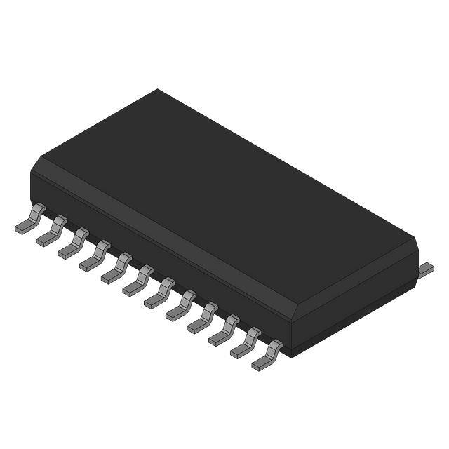
Package Diagram
24-Lead (300-Mil) Molded SOIC S13
SUNI is a trademark of PMC-Sierra, Incorporated. SST is a trademark of Cypress Semiconductor Corporation. All product and company names mentioned in this document are trademarks of their respective holders.
Document #: 38-02018 Rev. *B
Page 8 of 9
�CY7B952
Document History Page
Document Title: CY7B952 SST™ SONET/SDH Serial Transceiver Document Number: 38-02018 REV. ** *A *B ECN. 105981 122206 283371 Orig. of Issue Date Change 03/28/01 12/28/02 See ECN SZV RBI BCD Description of Change Change from Spec. number: 38-00502 to 38-02018 Add power up requirements to maximum ratings information. Removed Preliminary from the datasheet
Document #: 38-02018 Rev. *B
Page 9 of 9
�
很抱歉,暂时无法提供与“CY7B952-SC”相匹配的价格&库存,您可以联系我们找货
免费人工找货- 国内价格 香港价格
- 1+487.803551+50.22300
- 10+360.5470710+37.12100
- 50+330.8551950+34.06400
- 100+309.65225100+31.88100
- 500+303.29040500+31.22600
- 1000+294.801451000+30.35200
- 2000+292.684072000+30.13400
- 4000+290.556984000+29.91500


 工商网监
湘ICP备2023018690号
工商网监
湘ICP备2023018690号
