CY7C109BN, CY7C1009BN
128K x 8 Static RAM
Features
Functional Description
The CY7C109BN/CY7C1009BN[1] is a high performance CMOS
static RAM organized as 131,072 words by 8 bits. Easy memory
expansion is provided by an active LOW Chip Enable (CE1), an
active HIGH Chip Enable (CE2), an active LOW Output Enable
(OE), and three-state drivers. Writing to the device is accomplished by taking Chip Enable One (CE1) and Write Enable (WE)
inputs LOW and Chip Enable Two (CE2) input HIGH. Data on the
eight I/O pins (I/O0 through I/O7) is then written into the location
specified on the address pins (A0 through A16).
■
High Speed
❐ tAA = 15 ns
■
Low Active Power
❐ 440 mW (maximum 15 ns)
■
Low CMOS Standby Power
❐ 55 mW (maximum) 4 mW
■
2.0V Data Retention
■
Automatic Power Down when deselected
■
TTL-compatible Inputs and Outputs
■
Easy Memory Expansion with CE1, CE2, and OE options
Reading from the device is accomplished by taking Chip Enable
One (CE1) and Output Enable (OE) LOW while forcing Write
Enable (WE) and Chip Enable Two (CE2) HIGH. Under these
conditions, the contents of the memory location specified by the
address pins appear on the I/O pins.
The eight input/output pins (I/O0 through I/O7) are placed in a
high impedance state when the device is deselected (CE1 HIGH
or CE2 LOW), the outputs are disabled (OE HIGH), or during a
write operation (CE1 LOW, CE2 HIGH, and WE LOW).
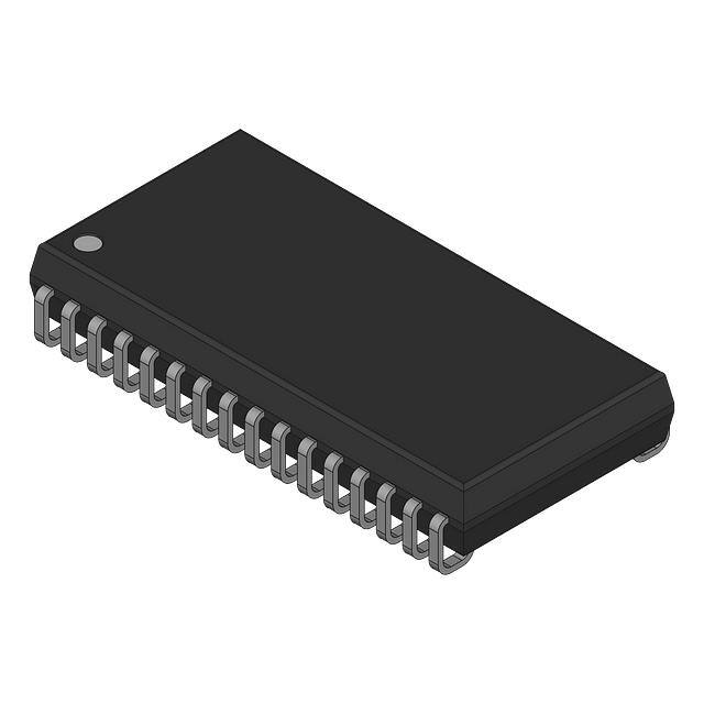
The CY7C109BN is available in standard 400-mil-wide SOJ and
32-pin TSOP type I packages. The CY7C1009BN is available in
a 300-mil-wide SOJ package. The CY7C1009BN and
CY7C109BN are functionally equivalent in all other respects.
Logic Block Diagram
I/O0
INPUT BUFFER
OE
SEN SE AMPS
I/O2
512x 256 x 8
ARRAY
I/O3
I/O4
I/O5
POWER
DOWN
COLUMN
DECODER
I/O6
I/O7
A9
A10
A11
A1 2
A1 3
A1 4
A1 5
A1 6
CE1
CE2
WE
I/O1
R OW DECODER
A0
A1
A2
A3
A4
A5
A6
A7
A8
Note
1. For guidelines on SRAM system design, refer to the ‘System Design Guidelines’ Cypress application note, available on the internet at www.cypress.com.
Cypress Semiconductor Corporation
Document #: 001-06430 Rev. *B
•
198 Champion Court
•
San Jose, CA 95134-1709
•
408-943-2600
Revised April 5, 2010
[+] Feedback
�CY7C109BN, CY7C1009BN
Pin Configurations
Figure 1. 32-Pin SOJ (TopView)
NC
A16
A14
A12
A7
A6
A5
A4
A3
A2
A1
32
31
30
29
28
27
26
25
24
23
22
21
20
19
18
17
1
2
3
4
5
6
7
8
9
10
11
A0
I/O0
I/O1
I/O2
GND
13
14
15
16
VCC
A15
CE2
WE
A13
A8
A9
A11
OE
A10
CE1
I/O7
I/O6
I/O5
I/O4
I/O3
Selection Guide
7C109B-15
7C1009B-15
7C109B-20
7C1009B-20
Unit
Maximum Access Time
15
20
ns
Maximum Operating Current
80
75
mA
Maximum CMOS Standby Current
10
10
mA
2
2
mA
Description
L
Document #: 001-06430 Rev. *B
Page 2 of 9
[+] Feedback
�CY7C109BN, CY7C1009BN
Maximum Ratings
Exceeding maximum ratings may shorten the useful life of the
device. User guidelines are not tested.
Current into Outputs (LOW)......................................... 20 mA
Static Discharge Voltage............................................ >2001V
(per MIL-STD-883, Method 3015)
Storage Temperature ................................. –65C to +150C
Ambient Temperature with
Power Applied ............................................ –55C to +125C
Latch Up Current ..................................................... >200 mA
Operating Range
Supply Voltage on VCC to Relative GND[2] .....–0.5V to +7.0V
DC Voltage Applied to Outputs
in High Z State[2] .................................... –0.5V to VCC + 0.5V
Ambient
Temperature
VCC
0C to +70C
5V 10%
40C to +85C
5V 10%
Range
Commercial
DC Input Voltage[2] ................................ –0.5V to VCC + 0.5V
Industrial
Electrical Characteristics Over the Operating Range
Parameter
Description
7C109BN-15
7C1009BN-15
Test Conditions
Min
VOH
Output HIGH Voltage
VCC = Min, IOH = –4.0 mA
VOL
Output LOW Voltage
VCC = Min, IOL = 8.0 mA
VIH
Input HIGH Voltage
Max
2.4
7C109BN-20
7C1009BN-20
Min
2.4
0.4
Voltage[2]
Unit
Max
V
0.4
V
2.2
VCC + 0.3
2.2
VCC + 0.3
V
–0.3
0.8
–0.3
0.8
V
VIL
Input LOW
IIX
Input Leakage
Current
GND < VI < VCC
–1
+1
–1
+1
A
IOZ
Output Leakage
Current
GND < VI < VCC,
Output Disabled
–5
+5
–5
+5
A
IOS
Output Short
Circuit Current[3]
VCC = Max, VOUT = GND
–300
–300
mA
ICC
VCC Operating
Supply Current
VCC = Max, IOUT = 0 mA,
f = fMAX = 1/tRC
80
75
mA
ISB1
Automatic CE
Power Down Current
—TTL Inputs
Max VCC, CE1 > VIH
or CE2 < VIL, VIN > VIH or
VIN < VIL, f = fMAX
40
30
mA
ISB2
Automatic CE
Power Down Current
—CMOS Inputs
Max VCC,
CE1 > VCC – 0.3V,
or CE2 < 0.3V,
VIN > VCC – 0.3V,
or VIN < 0.3V, f = 0
10
10
mA
2
2
mA
L
Capacitance
The following are the input and outpiut capacitance test conditions.[4]
Parameter
Description
CIN
Input Capacitance
COUT
Output Capacitance
Test Conditions
TA = 25C, f = 1 MHz,
VCC = 5.0V
Max
Unit
9
pF
8
pF
Notes
2. Minimum voltage is –2.0V for pulse durations of less than 20 ns.
3. Not more than one output should be shorted at one time. Duration of the short circuit should not exceed 30 seconds.
4. Tested initially and after any design or process changes that may affect these parameters.
Document #: 001-06430 Rev. *B
Page 3 of 9
[+] Feedback
�CY7C109BN, CY7C1009BN
Figure 2. AC Test Loads and Waveforms
R1 480
5V
R1 480
5V
OUTPUT
ALL INPUT PULSES
3.0V
90%
OUTPUT
30 pF
R2
255
R2
255
5 pF
INCLUDING
JIG AND
SCOPE
(a)
90%
10%
10%
GND
3 ns
INCLUDING
JIG AND
SCOPE
(b)
3 ns
THÉVENIN EQUIVALENT
167
1.73V
OUTPUT
Equivalent to:
Switching Characteristics[5] Over the Operating Range
Parameter
Description
7C109BN-15
7C1009BN-15
7C109BN-20
7C1009BN-20
Min
Min
Max
Unit
Max
Read Cycle
tRC
Read Cycle Time
15
20
tAA
Address to Data Valid
tOHA
Data Hold from Address Change
tACE
CE1 LOW to Data Valid, CE2 HIGH to Data Valid
15
20
ns
tDOE
OE LOW to Data Valid
7
8
ns
tLZOE
OE LOW to Low Z
tHZOE
OE HIGH to High Z[6, 7]
15
3
20
3
0
tLZCE
CE1 LOW to Low Z, CE2 HIGH to Low
tHZCE
CE1 HIGH to High Z, CE2 LOW to High Z[6, 7]
tPU
CE1 LOW to Power Up, CE2 HIGH to Power Up
tPD
CE1 HIGH to Power Down, CE2 LOW to
Power Down
3
ns
8
3
7
0
ns
ns
8
0
15
ns
ns
0
7
Z[7]
ns
ns
ns
20
ns
Write Cycle[8]
tWC
Write Cycle Time[9]
15
20
ns
tSCE
CE1 LOW to Write End, CE2 HIGH to Write End
12
15
ns
tAW
Address Setup to Write End
12
15
ns
tHA
Address Hold from Write End
0
0
ns
tSA
Address Setup to Write Start
0
0
ns
tPWE
WE Pulse Width
12
12
ns
tSD
Data Setup to Write End
8
10
ns
tHD
Data Hold from Write End
0
0
ns
Z[7]
tLZWE
WE HIGH to Low
tHZWE
WE LOW to High Z[6, 7]
3
3
7
ns
8
ns
Notes
5. Test conditions assume signal transition time of 3 ns or less, timing reference levels of 1.5V, input pulse levels of 0 to 3.0V, and output loading of the specified
IOL/IOH and 30-pF load capacitance.
6. tHZOE, tHZCE, and tHZWE are specified with a load capacitance of 5 pF as in part (b) of AC Test Loads. Transition is measured 500 mV from steady-state voltage.
7. At any given temperature and voltage condition, tHZCE is less than tLZCE, tHZOE is less than tLZOE, and tHZWE is less than tLZWE for any given device.
8. The internal write time of the memory is defined by the overlap of CE1 LOW, CE2 HIGH, and WE LOW. CE1 and WE must be LOW and CE2 HIGH to initiate a
write, and the transition of any of these signals can terminate the write. The input data setup and hold timing should be referenced to the leading edge of the
signal that terminates the write.
9. The minimum write cycle time for Write Cycle No. 3 (WE controlled, OE LOW) is the sum of tHZWE and tSD.
Document #: 001-06430 Rev. *B
Page 4 of 9
[+] Feedback
�CY7C109BN, CY7C1009BN
Data Retention Characteristics Over the Operating Range (Low Power version only)
Parameter
Description
VDR
VCC for Data Retention
Conditions
ICCDR
Data Retention Current
tCDR
Chip Deselect to Data Retention Time
tR
Operation Recovery Time
Min
No input may exceed VCC + 0.5V
VCC = VDR = 2.0V,
CE1 > VCC – 0.3V or CE2 < 0.3V,
VIN > VCC – 0.3V or VIN < 0.3V
Max
2.0
Unit
V
150
A
0
ns
200
s
Figure 3. Data Retention Waveform
DATA RETENTION MODE
VCC
4.5V
4.5V
VDR > 2V
tR
tCDR
CE
Switching Waveforms
Figure 4. Read Cycle No. 1[10, 11]
tRC
ADDRESS
tOHA
DATA OUT
tAA
PREVIOUS DATA VALID
DATA VALID
Figure 5. Read Cycle No. 2 (OE Controlled)[11, 12]
ADDRESS
tRC
CE1
CE2
tACE
OE
tHZOE
tDOE
DATA OUT
tLZOE
HIGH IMPEDANCE
tLZCE
VCC
SUPPLY
CURRENT
tHZCE
HIGH
IMPEDANCE
DATA VALID
tPD
tPU
50%
50%
ICC
ISB
Notes
10. Device is continuously selected. OE, CE1 = VIL, CE2 = VIH.
11. WE is HIGH for read cycle.
12. Address valid prior to or coincident with CE1 transition LOW and CE2 transition HIGH.
Document #: 001-06430 Rev. *B
Page 5 of 9
[+] Feedback
�CY7C109BN, CY7C1009BN
Switching Waveforms (continued)
Figure 6. Write Cycle No. 1 (CE1 or CE2 Controlled)[13, 14]
tWC
ADDRESS
tSCE
CE1
tSA
CE2
tSCE
tAW
tHA
tPWE
WE
tSD
DATA I/O
tHD
DATA VALID
Figure 7. Write Cycle No. 2 (WE Controlled, OE HIGH During Write)[13, 14]
tWC
ADDRESS
tSCE
CE1
CE2
tSCE
tAW
tSA
tHA
tPWE
WE
OE
tSD
DATA I/O
tHD
DATAIN VALID
NOTE 15
tHZOE
Notes
13. Data I/O is high impedance if OE = VIH.
14. If CE1 goes HIGH or CE2 goes LOW simultaneously with WE going HIGH, the output remains in a high-impedance state.
15. During this period the I/Os are in the output state and input signals should not be applied.
Document #: 001-06430 Rev. *B
Page 6 of 9
[+] Feedback
�CY7C109BN, CY7C1009BN
Switching Waveforms (continued)
Figure 8. Write Cycle No. 3 (WE Controlled, OE LOW)[14]
tWC
ADDRESS
tSCE
CE1
CE2
tSCE
tAW
tSA
tHA
tPWE
WE
tSD
NOTE 15
DATA I/O
tHD
DATA VALID
tLZWE
tHZWE
Truth Table
CE1
CE2
OE
WE
I/O0–I/O7
Mode
Power
H
X
X
X
High Z
Power Down
Standby (ISB)
X
L
X
X
High Z
Power Down
Standby (ISB)
L
H
L
H
Data Out
Read
Active (ICC)
L
H
X
L
Data In
Write
Active (ICC)
L
H
H
H
High Z
Selected, Outputs Disabled
Active (ICC)
Ordering Information
Speed
(ns)
Ordering Code
Package
Diagram
Package Type
Operating
Range
15
CY7C1009BN-15VI
51-85041
32-Pin (300-Mil) Molded SOJ
Industrial
20
CY7C109BN-20VI
51-85033
32-Pin (400-Mil) Molded SOJ
Industrial
Contact your local sales representative regarding availability of these parts
Document #: 001-06430 Rev. *B
Page 7 of 9
[+] Feedback
�CY7C109BN, CY7C1009BN
Package Diagrams
Figure 9. 32-Pin (300-Mil) Molded
51-85041 *B
Figure 10. 32-Pin (400-Mil) Molded SOJ
51-85033 *C
Document #: 001-06430 Rev. *B
Page 8 of 9
[+] Feedback
�CY7C109BN, CY7C1009BN
Document History Page
Document Title: CY7C109BN/CY7C1009BN 128K x 8 Static RAM
Document Number: 001-06430
REV.
ECN No.
Orig. of
Change
Submission Description of Change
Date
**
423847
NXR
See ECN
*A
2755340
NXR
08/24/2009
*B
2904565
AJU
04/05/10
New Data Sheet
Removed -12 from product offering as 12ns parts are not active
Corrected Package Diagram
Updated ordering Information
Removed inactive part number from the ordering information table.Updated
package diagrams.
Sales, Solutions, and Legal Information
Worldwide Sales and Design Support
Cypress maintains a worldwide network of offices, solution centers, manufacturer’s representatives, and distributors. To find the office
closest to you, visit us at cypress.com/sales.
Products
PSoC
Clocks & Buffers
psoc.cypress.com
clocks.cypress.com
Wireless
wireless.cypress.com
Memories
memory.cypress.com
Image Sensors
image.cypress.com
© Cypress Semiconductor Corporation, 2006-2010. The information contained herein is subject to change without notice. Cypress Semiconductor Corporation assumes no responsibility for the use of
any circuitry other than circuitry embodied in a Cypress product. Nor does it convey or imply any license under patent or other rights. Cypress products are not warranted nor intended to be used for
medical, life support, life saving, critical control or safety applications, unless pursuant to an express written agreement with Cypress. Furthermore, Cypress does not authorize its products for use as
critical components in life-support systems where a malfunction or failure may reasonably be expected to result in significant injury to the user. The inclusion of Cypress products in life-support systems
application implies that the manufacturer assumes all risk of such use and in doing so indemnifies Cypress against all charges.
Any Source Code (software and/or firmware) is owned by Cypress Semiconductor Corporation (Cypress) and is protected by and subject to worldwide patent protection (United States and foreign),
United States copyright laws and international treaty provisions. Cypress hereby grants to licensee a personal, non-exclusive, non-transferable license to copy, use, modify, create derivative works of,
and compile the Cypress Source Code and derivative works for the sole purpose of creating custom software and or firmware in support of licensee product to be used only in conjunction with a Cypress
integrated circuit as specified in the applicable agreement. Any reproduction, modification, translation, compilation, or representation of this Source Code except as specified above is prohibited without
the express written permission of Cypress.
Disclaimer: CYPRESS MAKES NO WARRANTY OF ANY KIND, EXPRESS OR IMPLIED, WITH REGARD TO THIS MATERIAL, INCLUDING, BUT NOT LIMITED TO, THE IMPLIED WARRANTIES
OF MERCHANTABILITY AND FITNESS FOR A PARTICULAR PURPOSE. Cypress reserves the right to make changes without further notice to the materials described herein. Cypress does not
assume any liability arising out of the application or use of any product or circuit described herein. Cypress does not authorize its products for use as critical components in life-support systems where
a malfunction or failure may reasonably be expected to result in significant injury to the user. The inclusion of Cypress’ product in a life-support systems application implies that the manufacturer
assumes all risk of such use and in doing so indemnifies Cypress against all charges.
Use may be limited by and subject to the applicable Cypress software license agreement.
Document #: 001-06430 Rev. *B
Revised April 5, 2010
Page 9 of 9
All products and company names mentioned in this document may be the trademarks of their respective holders.
[+] Feedback
�


 工商网监
湘ICP备2023018690号
工商网监
湘ICP备2023018690号
