CY7C185
64-Kbit (8 K × 8) Static RAM
64-Kbit (8 K × 8) Static RAM
Features
Functional Description
The CY7C185[1] is a high-performance CMOS static RAM
organized as 8192 words by 8 bits. Easy memory expansion is
provided by an active LOW chip enable (CE1), an active HIGH
chip enable (CE2), and active LOW output enable (OE) and
tri-state drivers. This device has an automatic power-down
feature (CE1 or CE2), reducing the power consumption by 70%
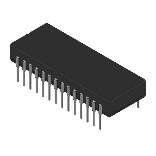
when deselected. The CY7C185 is in a standard 300-mil-wide
DIP, SOJ, or SOIC package.
■
High speed
❐ 15 ns
■
Fast tDOE
■
Low active power
❐ 715 mW
■
Low standby power
❐ 85 mW
■
CMOS for optimum speed/power
■
Easy memory expansion with CE1, CE2 and OE features
■
TTL-compatible inputs and outputs
■
Automatic power-down when deselected
■
Available in non Pb-free 28-pin (300-Mil) Molded SOJ, 28-pin
(300-Mil) Molded SOIC and Pb-free 28-pin (300-Mil) Molded
DIP
An active LOW write enable signal (WE) controls the
writing/reading operation of the memory. When CE1 and WE
inputs are both LOW and CE2 is HIGH, data on the eight data
input/output pins (I/O0 through I/O7) is written into the memory
location addressed by the address present on the address pins
(A0 through A12). Reading the device is accomplished by
selecting the device and enabling the outputs, CE1 and OE
active LOW, CE2 active HIGH, while WE remains inactive or
HIGH. Under these conditions, the contents of the location
addressed by the information on address pins are present on the
eight data input or output pins.
The input or output pins remain in a high-impedance state unless
the chip is selected, outputs are enabled, and write enable (WE)
is HIGH. A die coat is used to insure alpha immunity.
Logic Block Diagram
I/O0
I/O1
I/O2
SENSE AMPS
A1
A2
A3
A4
A5
A6
A7
A8
ROW DECODER
INPUT BUFFER
8K x 8
ARRAY
I/O3
I/O4
I/O5
I/O6
CE1
CE2
WE
COLUMN DECODER
POWER
DOWN
I/O7
A12
A11
A10
A0
A9
OE
Note
1. For guidelines on SRAM system design, please refer to the ‘System Design Guidelines’ Cypress application note, available on the internet at www.cypress.com.
Cypress Semiconductor Corporation
Document Number: 38-05043 Rev. *F
•
198 Champion Court
•
San Jose, CA 95134-1709
•
408-943-2600
Revised May 19, 2014
�CY7C185
Contents
Pin Configuration ............................................................. 3
Selection Guide ................................................................ 3
Maximum Ratings ............................................................. 4
Operating Range ............................................................... 4
Electrical Characteristics ................................................. 4
Capacitance ...................................................................... 5
AC Test Loads and Waveforms ....................................... 5
Switching Characteristics ................................................ 6
Switching Waveforms ...................................................... 7
Typical DC and AC Characteristics .............................. 10
Truth Table ...................................................................... 11
Address Designators ..................................................... 11
Ordering Information ...................................................... 12
Ordering Code Definitions ......................................... 12
Document Number: 38-05043 Rev. *F
Package Diagrams .......................................................... 13
Acronyms ........................................................................ 16
Document Conventions ................................................. 16
Units of Measure ....................................................... 16
Document History Page ................................................. 17
Sales, Solutions, and Legal Information ...................... 18
Worldwide Sales and Design Support ....................... 18
Products .................................................................... 18
PSoC® Solutions ...................................................... 18
Cypress Developer Community ................................. 18
Technical Support ..................................................... 18
Page 2 of 18
�CY7C185
Pin Configuration
Figure 1. 28-pin DIP / SOJ pinout (Top View)
DIP/SOJ
Top View
NC
A4
A5
A6
A7
A8
A9
A10
A11
A12
I/O0
I/O1
I/O2
GND
1
2
3
4
5
6
7
8
9
10
11
12
13
14
28
27
26
25
24
23
22
21
20
19
18
17
16
15
VCC
WE
CE2
A3
A2
A1
OE
A0
CE1
I/O7
I/O6
I/O5
I/O4
I/O3
Selection Guide
Description
-15
-20
-35
Maximum Access Time (ns)
15
20
35
Maximum Operating Current (mA)
130
110
100
Maximum CMOS Standby Current (mA)
15
15
15
Document Number: 38-05043 Rev. *F
Page 3 of 18
�CY7C185
Maximum Ratings
Output current into outputs (LOW) ............................. 20 mA
Exceeding maximum ratings may shorten the useful life of the
device. User guidelines are not tested.
Storage temperature ................................ –65 C to +150 C
Ambient temperature with
power applied .......................................... –55 C to +125 C
Static discharge voltage
(per MIL-STD-883, Method 3015) .......................... >2001 V
Latch-up current .................................................... >200 mA
Operating Range
Supply voltage to ground potential ..............–0.5 V to +7.0 V
Range
DC voltage applied to outputs
in High Z State [2] .........................................–0.5 V to +7.0 V
Commercial
DC input voltage [2] ......................................–0.5 V to +7.0 V
Ambient Temperature
VCC
0 °C to +70 °C
5 V 10%
–40 °C to +85 °C
5 V 10%
Industrial
Electrical Characteristics
Over the Operating Range
Parameter
Description
Test Conditions
VOH
Output HIGH Voltage
VCC = Min.,
IOH = –4.0 mA
VOL
Output LOW Voltage
VCC = Min.,
IOL = 8.0 mA
VIH
Input HIGH Voltage
[2]
-15
-20
-35
Unit
Min
Max
Min
Max
Min
Max
2.4
–
2.4
–
2.4
–
V
–
0.4
–
0.4
–
0.4
V
2.2
VCC + 0.3
2.2
VCC + 0.3
2.2
VCC + 0.3
V
VIL
Input LOW Voltage
–0.5
0.8
–0.5
0.8
–0.5
0.8
V
IIX
Input Leakage Current
GND VI VCC
–5
+5
–5
+5
–5
+5
A
IOZ
Output Leakage Current
GND VI VCC,
Output Disabled
–5
+5
–5
+5
–5
+5
A
ICC
VCC Operating Supply
Current
VCC = Max.,
IOUT = 0 mA
–
130
–
110
–
100
mA
ISB1
Automatic Power-down
Current
Max. VCC,
–
40
–
20
–
20
mA
–
15
–
15
–
15
mA
CE1 VIH or CE2 VIL,
Min. Duty Cycle =100%
ISB2
Automatic Power-down
Current
Max. VCC,
CE1 VCC – 0.3 V or
CE2 0.3 V,
VIN VCC – 0.3 V or
VIN 0.3 V
Note
2. Minimum voltage is equal to –3.0 V for pulse durations less than 30 ns.
Document Number: 38-05043 Rev. *F
Page 4 of 18
�CY7C185
Capacitance
Parameter [3]
Description
CIN
Input capacitance
COUT
Output capacitance
Test Conditions
TA = 25 C, f = 1 MHz, VCC = 5.0 V
Max
Unit
7
pF
7
pF
AC Test Loads and Waveforms
Figure 2. AC Test Loads and Waveforms
R1 481
5V
OUTPUT
30 pF
INCLUDING
JIG AND
SCOPE
R1 481
5V
OUTPUT
R2
255
(a)
ALL INPUT PULSES
3.0 V
5 pF
INCLUDING
JIGAND
SCOPE
R2
255
(b)
GND
10%
5 ns
Equivalent to:
OUTPUT
90%
90%
10%
5 ns
THÉVENIN EQUIVALENT
167
1.73 V
Note
3. Tested initially and after any design or process changes that may affect these parameters.
Document Number: 38-05043 Rev. *F
Page 5 of 18
�CY7C185
Switching Characteristics
Over the Operating Range
Parameter [4]
Description
-15
-20
-35
Min
Max
Min
Max
Min
Max
Unit
Read Cycle
tRC
Read Cycle Time
15
–
20
–
35
–
ns
tAA
Address to Data Valid
–
15
–
20
–
35
ns
tOHA
Data Hold from Address Change
3
–
5
–
5
–
ns
tACE1
CE1 LOW to Data Valid
–
15
–
20
–
35
ns
tACE2
CE2 HIGH to Data Valid
–
15
–
20
–
35
ns
tDOE
OE LOW to Data Valid
–
8
–
9
–
15
ns
tLZOE
OE LOW to Low Z
3
–
3
–
3
–
ns
tHZOE
OE HIGH to High Z
[5]
–
7
–
8
–
10
ns
tLZCE1
CE1 LOW to Low Z [6]
3
–
5
–
5
–
ns
tLZCE2
CE2 HIGH to Low Z
3
–
3
–
3
–
ns
–
7
–
8
–
10
ns
[5, 6]
tHZCE
CE1 HIGH to High Z
CE2 LOW to High Z
tPU
CE1 LOW to Power-up
CE2 to HIGH to Power-up
0
–
0
–
0
–
ns
tPD
CE1 HIGH to Power-down
CE2 LOW to Power-down
–
15
–
20
–
20
ns
Write Cycle [7, 8]
tWC
Write Cycle Time
15
–
20
–
35
–
ns
tSCE1
CE1 LOW to Write End
12
–
15
–
20
–
ns
tSCE2
CE2 HIGH to Write End
12
–
15
–
20
–
ns
tAW
Address Setup to Write End
12
–
15
–
25
–
ns
tHA
Address Hold from Write End
0
–
0
–
0
–
ns
tSA
Address Setup to Write Start
0
–
0
–
0
–
ns
tPWE
WE Pulse Width
12
–
15
–
20
–
ns
tSD
Data Setup to Write End
8
–
10
–
12
–
ns
tHD
Data Hold from Write End
0
–
0
–
0
–
ns
–
7
–
7
–
8
ns
3
–
5
–
5
–
ns
tHZWE
WE LOW to High Z
tLZWE
WE HIGH to Low Z
[5]
Notes
4. Test conditions assume signal transition time of 5 ns or less, timing reference levels of 1.5 V, input pulse levels of 0 to 3.0 V, and output loading of the specified IOL/IOH
and 30-pF load capacitance.
5. tHZOE, tHZCE, and tHZWE are specified with CL = 5 pF as in part (b) of AC Test Loads. Transition is measured 500 mV from steady state voltage.
6. At any temperature and voltage condition, tHZCE is less than tLZCE1 and tLZCE2 for any given device.
7. The internal write time of the memory is defined by the overlap of CE1 LOW, CE2 HIGH, and WE LOW. All 3 signals must be active to initiate a write and either signal
can terminate a write by going HIGH. The data input setup and hold timing must be referenced to the rising edge of the signal that terminates the write.
8. The minimum write cycle pulse width of Write cycle No. 3 (WE Controlled, OE LOW) should be equal to sum tHZWE and tSD.
Document Number: 38-05043 Rev. *F
Page 6 of 18
�CY7C185
Switching Waveforms
Figure 3. Read Cycle No. 1 [9, 10]
tRC
ADDRESS
tAA
tOHA
DATA OUT
PREVIOUS DATA VALID
DATA VALID
Figure 4. Read Cycle No. 2 [11, 12]
tRC
CE1
CE2
tACE
OE
OE
tHZOE
tDOE
DATA OUT
tLZOE
HIGH IMPEDANCE
tLZCE
VCC
SUPPLY
CURRENT
tHZCE
HIGH
IMPEDANCE
DATA VALID
tPD
tPU
ICC
50%
50%
ISB
Notes
9. Device is continuously selected. OE, CE1 = VIL. CE2 = VIH.
10. WE is HIGH for read cycle.
11. Data I/O is High Z if OE = VIH, CE1 = VIH, WE = VIL, or CE2=VIL.
12. The internal write time of the memory is defined by the overlap of CE1 LOW, CE2 HIGH and WE LOW. CE1 and WE must be LOW and CE2 must be HIGH to initiate
write. A write can be terminated by CE1 or WE going HIGH or CE2 going LOW. The data input setup and hold timing must be referenced to the rising edge of the
signal that terminates the write.
Document Number: 38-05043 Rev. *F
Page 7 of 18
�CY7C185
Switching Waveforms (continued)
Figure 5. Write Cycle No. 1 (WE Controlled) [13, 14]
tWC
ADDRESS
tSCEI
CE1
tAW
CE
CE
2
WE
tHA
tSCE2
tSA
tPWE
OE
tSD
DATA I/O
tHD
DATA IN VALID
NOTE 15
tHZOE
Figure 6. Write Cycle No. 2 (CE Controlled) [14, 15, 16]
tWC
ADDRESS
tSCE1
CE1
tSA
CE2
tSCE2
tAW
tHA
WE
tSD
DATA I/O
tHD
DATA IN VALID
Notes
13. WE is HIGH for read cycle.
14. The internal write time of the memory is defined by the overlap of CE1 LOW, CE2 HIGH and WE LOW. CE1 and WE must be LOW and CE2 must be HIGH to initiate
write. A write can be terminated by CE1 or WE going HIGH or CE2 going LOW. The data input setup and hold timing must be referenced to the rising edge of the
signal that terminates the write.
15. During this period, the I/Os are in the output state and input signals must not be applied.
16. The minimum write cycle time for Write Cycle #3 (WE Controlled, OE LOW) is the sum of tHZWE and tSD.
Document Number: 38-05043 Rev. *F
Page 8 of 18
�CY7C185
Switching Waveforms (continued)
Figure 7. Write Cycle No. 3 (WE Controlled, OE LOW) [17, 19, 20]
tWC
ADDRESS
CE1
tSCE1
CE2
tSCE2
tAW
WE
tHA
tSA
tSD
DATA I/O
NOTE 18
tHD
DATA IN VALID
tHZWE
tLZWE
Notes
17. The internal write time of the memory is defined by the overlap of CE1 LOW, CE2 HIGH and WE LOW. CE1 and WE must be LOW and CE2 must be HIGH to initiate
write. A write can be terminated by CE1 or WE going HIGH or CE2 going LOW. The data input setup and hold timing must be referenced to the rising edge of the
signal that terminates the write.
18. During this period, the I/Os are in the output state and input signals must not be applied.
19. The minimum write cycle time for Write Cycle #3 (WE Controlled, OE LOW) is the sum of tHZWE and tSD.
20. If CE1 goes HIGH or CE2 goes LOW simultaneously with WE HIGH, the output remains in a high-impedance state.
Document Number: 38-05043 Rev. *F
Page 9 of 18
�CY7C185
SB
I CC
0.8
0.6
0.4
4.5
5.0
0.8
0.6
0.4
V CC=5.0 V
V IN=5.0 V
5.5
ISB
0.0
–55
6.0
NORMALIZED ACCESS TIME
vs. AMBIENT TEMPERATURE
1.4
1.6
1.3
1.4
NORMALIZED t AA
NORMALIZED t AA
NORMALIZED ACCESS TIME
vs. SUPPLY VOLTAGE
1.2
TA =25C
1.0
1.2
1.0
VCC =5.0 V
0.8
0.9
0.8
4.0
4.5
5.0
5.5
SUPPLY VOLTAGE (V)
0.6
–55
6.0
2.5
25.0
DELTA tAA (ns)
30.0
2.0
1.5
1.0
25
2.0
3.0
4.0
80
VCC =5.0 V
TA =25C
60
40
20
0
0.0
15.0
10.0
VCC =4.5 V
TA =25C
5.0
SUPPLY VOLTAGE (V)
Document Number: 38-05043 Rev. *F
0.0
0
200
400
600
800 1000
CAPACITANCE (pF)
2.0
3.0
4.0
140
OUTPUT SINK CURRENT
vs. OUTPUT VOLTAGE
120
100
VCC =5.0 V
TA =25C
80
60
40
20
0
0.0
125
20.0
1.0
OUTPUT VOLTAGE (V)
1.25
5.0
0.5
1.0
100
TYPICAL ACCESS TIME CHANGE
vs. OUTPUT LOADING
3.0
0.0
0.0
120
AMBIENT TEMPERATURE (C)
TYPICAL POWER-ON CURRENT
vs. SUPPLY VOLTAGE
NORMALIZED I PO
125
OUTPUT SOURCE CURRENT
vs. OUTPUT VOLTAGE
AMBIENT TEMPERATURE (C)
SUPPLY VOLTAGE (V)
1.1
25
OUTPUT SINK CURRENT (mA)
0.0
4.0
I CC
0.2
I SB
0.2
1.0
NORMALIZED I CC
1.0
1.2
NORMALIZED I,CC
I
SB
1.2
NORMALIZED I,CCI
1.4
NORMALIZED SUPPLY CURRENT
vs. AMBIENT TEMPERATURE
NORMALIZED SUPPLY CURRENT
vs. SUPPLY VOLTAGE
OUTPUT SOURCE CURRENT (mA)
Typical DC and AC Characteristics
1.0
2.0
3.0
OUTPUT VOLTAGE (V)
4.0
NORMALIZED I CC vs. CYCLE TIME
VCC =5.0 V
TA =25C
VCC =0.5 V
1.00
0.75
0.50
10
20
30
40
CYCLE FREQUENCY (MHz)
Page 10 of 18
�CY7C185
Truth Table
CE1 CE2
Address Designators
WE
OE
Input/Output
Mode
Address Name
Address Function
Pin Number
A4
X3
2
A5
X4
3
A6
X5
4
H
X
X
X
High Z
Deselect/
Power-down
X
L
X
X
High Z
Deselect/
Power-down
L
H
H
L
Data Out
Read
A7
X6
5
L
H
L
X
Data In
Write
A8
X7
6
L
H
H
H
High Z
Deselect
A9
Y1
7
A10
Y4
8
A11
Y3
9
A12
Y0
10
A0
Y2
21
A1
X0
23
A2
X1
24
A3
X2
25
Document Number: 38-05043 Rev. *F
Page 11 of 18
�CY7C185
Ordering Information
Speed
(ns)
Package
Name
Ordering Code
Package Type
Operating
Range
15
CY7C185-15VI
51-85031 28-pin SOJ
20
CY7C185-20PXC
51-85014 28-pin PDIP (Pb-free)
Commercial
Industrial
35
CY7C185-35SC
51-85026 28-pin SOIC
Commercial
Ordering Code Definitions
CY 7 C 1 85 - XX X
X
X
Temperature Range: X = C or I
C = Commercial; I = Industrial
Pb-free
Package Type: X = V or P or S
V = 28-pin SOJ
P = 28-pin PDIP
S = 28-pin SOIC
Speed: XX = 15 ns or 20 ns or 35 ns
85 = 64 Kbit density with data width × 8 bits
Family Code: 1 = Fast Asynchronous SRAM family
Technology Code: C = CMOS
Marketing Code: 7 = SRAM
Company ID: CY = Cypress
Document Number: 38-05043 Rev. *F
Page 12 of 18
�CY7C185
Package Diagrams
Figure 8. 28-pin PDIP (300 Mil) Package Outline, 51-85014
51-85014 *G
Document Number: 38-05043 Rev. *F
Page 13 of 18
�CY7C185
Package Diagrams (continued)
Figure 9. 28-pin SOIC (0.713 × 0.300 × 0.0932 Inches) Package Outline, 51-85026
51-85026 *H
Document Number: 38-05043 Rev. *F
Page 14 of 18
�CY7C185
Package Diagrams (continued)
Figure 10. 28-pin SOJ (300 Mils) Package Outline, 51-85031
51-85031 *E
Document Number: 38-05043 Rev. *F
Page 15 of 18
�CY7C185
Acronyms
Acronym
Document Conventions
Description
Units of Measure
CE
Chip Enable
CMOS
Complementary Metal Oxide Semiconductor
°C
degree Celsius
I/O
Input/Output
MHz
megahertz
OE
Output Enable
µA
microampere
SRAM
Static Random Access Memory
mA
milliampere
SOJ
Small Outline J-Lead
mV
millivolt
TSOP
Thin Small Outline Package
mW
milliwatt
VFBGA
Very Fine-Pitch Ball Grid Array
ns
nanosecond
WE
Write Enable
pF
picofarad
V
volt
W
watt
Document Number: 38-05043 Rev. *F
Symbol
Unit of Measure
Page 16 of 18
�CY7C185
Document History Page
Document Title: CY7C185, 64-Kbit (8 K × 8) Static RAM
Document Number: 38-05043
Revision
ECN
Submission
Date
Orig. of
Change
**
107145
09/10/01
SZV
Change from Spec number: 38-00037 to 38-05043
Description of Change
*A
116470
09/16/02
CEA
Add applications foot note to data sheet
*B
486744
See ECN
NXR
Changed Low standby power from 220 mW to 85 mW
Changed the description of IIX from Input Load Current to Input Leakage
Current in DC Electrical Characteristics table
Removed IOS parameter from DC Electrical Characteristics table
Updated the Ordering Information table
*C
2263686
See ECN
VKN /
AESA
*D
3105329
12/09/2010
AJU
Removed 25 ns speed bin
Updated the Ordering Information table as per the current product offerings
Added Ordering Code Definitions.
Updated Package Diagrams.
*E
3235800
04/20/2011
PRAS
Updated package diagram spec 51-85026 to *F.
Added Acronyms and Units of Measure.
Template changes.
*F
4383597
05/19/2014
VINI
Updated Switching Characteristics:
Added Note 8 and referred the same note in “Write Cycle”.
Updated Package Diagrams:
spec 51-85014 – Changed revision from *E to *G.
spec 51-85026 – Changed revision from *F to *H.
spec 51-85031 – Changed revision from *D to *E.
Updated in new template.
Completing Sunset Review.
Document Number: 38-05043 Rev. *F
Page 17 of 18
�CY7C185
Sales, Solutions, and Legal Information
Worldwide Sales and Design Support
Cypress maintains a worldwide network of offices, solution centers, manufacturer’s representatives, and distributors. To find the office
closest to you, visit us at Cypress Locations.
PSoC® Solutions
Products
Automotive
Clocks & Buffers
Interface
Lighting & Power Control
cypress.com/go/automotive
cypress.com/go/clocks
cypress.com/go/interface
cypress.com/go/powerpsoc
cypress.com/go/plc
Memory
cypress.com/go/memory
PSoC
cypress.com/go/psoc
Touch Sensing
PSoC 1 | PSoC 3 | PSoC 4 | PSoC 5LP
Cypress Developer Community
Community | Forums | Blogs | Video | Training
Technical Support
cypress.com/go/support
cypress.com/go/touch
USB Controllers
Wireless/RF
psoc.cypress.com/solutions
cypress.com/go/USB
cypress.com/go/wireless
© Cypress Semiconductor Corporation, 2001-2014. The information contained herein is subject to change without notice. Cypress Semiconductor Corporation assumes no responsibility for the use of
any circuitry other than circuitry embodied in a Cypress product. Nor does it convey or imply any license under patent or other rights. Cypress products are not warranted nor intended to be used for
medical, life support, life saving, critical control or safety applications, unless pursuant to an express written agreement with Cypress. Furthermore, Cypress does not authorize its products for use as
critical components in life-support systems where a malfunction or failure may reasonably be expected to result in significant injury to the user. The inclusion of Cypress products in life-support systems
application implies that the manufacturer assumes all risk of such use and in doing so indemnifies Cypress against all charges.
Any Source Code (software and/or firmware) is owned by Cypress Semiconductor Corporation (Cypress) and is protected by and subject to worldwide patent protection (United States and foreign),
United States copyright laws and international treaty provisions. Cypress hereby grants to licensee a personal, non-exclusive, non-transferable license to copy, use, modify, create derivative works of,
and compile the Cypress Source Code and derivative works for the sole purpose of creating custom software and or firmware in support of licensee product to be used only in conjunction with a Cypress
integrated circuit as specified in the applicable agreement. Any reproduction, modification, translation, compilation, or representation of this Source Code except as specified above is prohibited without
the express written permission of Cypress.
Disclaimer: CYPRESS MAKES NO WARRANTY OF ANY KIND, EXPRESS OR IMPLIED, WITH REGARD TO THIS MATERIAL, INCLUDING, BUT NOT LIMITED TO, THE IMPLIED WARRANTIES
OF MERCHANTABILITY AND FITNESS FOR A PARTICULAR PURPOSE. Cypress reserves the right to make changes without further notice to the materials described herein. Cypress does not
assume any liability arising out of the application or use of any product or circuit described herein. Cypress does not authorize its products for use as critical components in life-support systems where
a malfunction or failure may reasonably be expected to result in significant injury to the user. The inclusion of Cypress’ product in a life-support systems application implies that the manufacturer
assumes all risk of such use and in doing so indemnifies Cypress against all charges.
Use may be limited by and subject to the applicable Cypress software license agreement.
Document Number: 38-05043 Rev. *F
Revised May 19, 2014
All products and company names mentioned in this document may be the trademarks of their respective holders.
Page 18 of 18
�


 工商网监
湘ICP备2023018690号
工商网监
湘ICP备2023018690号
