CY7C4281V/CY7C4291V CY7C4261V/CY7C4271V16K/32K/64K/128K x 9 Low-Voltage Deep Sync™ FIFOs
CY7C4261V/CY7C4271V CY7C4281V/CY7C4291V
16K/32K/64K/128K x 9 Low-Voltage Deep Sync™ FIFOs
Features
• 3.3V operation for low power consumption and easy integration into low-voltage systems • High-speed, low-power, first-in first-out (FIFO) memories • 16K × 9 (CY7C4261V) • 32K × 9 (CY7C4271V) • 64K × 9 (CY7C4281V) • 128K × 9 (CY7C4291V) • 0.35-micron CMOS for optimum speed/power • High-speed 100-MHz operation (10-ns read/write cycle times) • Low power — ICC = 25 mA — ISB = 4 mA • Fully asynchronous and simultaneous read and write operation • Empty, Full, and programmable Almost Empty and Almost Full status flags • Output Enable (OE) pin • Independent read and write enable pins • Supports free-running 50% duty cycle clock inputs • Width- Expansion capability • Pin-compatible 3.3V solutions for CY7C4261/71/81/91 • Pin-compatible density upgrade to CY7C42X1V family • Pb-Free Packages Available
Functional Description
The CY7C4261/71/81/91V are high-speed, low-power FIFO memories with clocked read and write interfaces. All are nine bits wide. The CY7C4261/71/81/91V are pin-compatible to the CY7C42x1V Synchronous FIFO family. Programmable features include Almost Full/Almost Empty flags. These FIFOs provide solutions for a wide variety of data buffering needs, including high-speed data acquisition, multiprocessor interfaces, and communications buffering. These FIFOs have 9-bit input and output ports that are controlled by separate clock and enable signals. The input port is controlled by a free-running clock (WCLK) and two write-enable pins (WEN1, WEN2/LD). When WEN1 is LOW and WEN2/LD is HIGH, data is written into the FIFO on the rising edge of the WCLK signal. While WEN1 and WEN2/LD are held active, data is continually written into the FIFO on each WCLK cycle. The output port is controlled in a similar manner by a free-running read clock (RCLK) and two read enable pins (REN1, REN2). In addition, the CY7C4261/71/81/91V has an output enable pin (OE). The read (RCLK) and write (WCLK) clocks may be tied together for single-clock operation or the two clocks may be run independently for asynchronous read/write applications. Clock frequencies up to 100 MHz are achievable. Depth expansion is possible using one enable input for system control, while the other enable is controlled by expansion logic to direct the flow of data.
LogicBlock Diagram
D0–8 INPUT REGISTER
Pin Configuration
PLCC Top View
D2 D3 D4 D5 D6 D7 D8
WCLK WEN1 WEN2/LD FLAG PROGRAM REGISTER WRITE CONTROL FLAG LOGIC READ POINTER EF PAE PAF FF
D1 D0 PAF PAE GND REN1 RCLK REN2 OE
WRITE POINTER RESET LOGIC
Dual Port RAM Array 16K/32K 64K/128K x9
5 6 7 8 9 10 11 12 13
4 3 2 1 32 31 30 29 28
25 24 23 22 21 14 15 16 17 18 19 20 EF FF Q0 Q1 Q2 Q3 Q4
CY7C4261V CY7C4271V CY7C4281V CY7C4291V
27 26
RS WEN1 WCLK WEN2/LD VCC Q8 Q7 Q6 Q5
RS
THREE-STATE OUTPUT REGISTER OE Q0–8
READ CONTROL
RCLK REN1 REN2
Cypress Semiconductor Corporation Document #: 38-06013 Rev. *B
•
3901 North First Street
•
San Jose, CA 95134 • 408-943-2600 Revised August 2, 2005
�CY7C4261V/CY7C4271V CY7C4281V/CY7C4291V
Selection Guide
7C4261/71/81/91V-10 Maximum Frequency Maximum Access Time Minimum Cycle Time Minimum Data or Enable Set-up Minimum Data or Enable Hold Maximum Flag Delay Active Power Supply Current (ICC1) Commercial Industrial CY7C4261V Density Package 16K x 9 32-pin PLCC CY7C4271V 32K x 9 32-pin PLCC 100 8 10 3.5 0 8 25 7C4261/71/81/91V-15 66.7 10 15 4 0 10 25 30 CY7C4281V 64K x 9 32-pin PLCC CY7C4291V 128K x 9 32-pin PLCC 7C4261/71/81/91V-25 40 15 25 6 1 15 25 Unit MHz ns ns ns ns ns mA
Pin Definitions
Signal Name D0−8 Q0−8 WEN1 Description Data Inputs Data Outputs Write Enable 1 I/O I O I Data Inputs for 9-bit bus. Data Outputs for 9-bit bus. The only write enable when device is configured to have programmable flags. Data is written on a LOW-to-HIGH transition of WCLK when WEN1 is asserted and FF is HIGH. If the FIFO is configured to have two write enables, data is written on a LOW-to-HIGH transition of WCLK when WEN1 is LOW and WEN2/LD and FF are HIGH. If HIGH at reset, this pin operates as a second write enable. If LOW at reset, this pin operates as a control to write or read the programmable flag offsets. WEN1 must be LOW and WEN2 must be HIGH to write data into the FIFO. Data will not be written into the FIFO if the FF is LOW. If the FIFO is configured to have programmable flags, WEN2/LD is held LOW to write or read the programmable flag offsets. Enables the device for Read operation. Both REN1 and REN2 must be asserted to allow a read operation. The rising edge clocks data into the FIFO when WEN1 is LOW and WEN2/LD is HIGH and the FIFO is not Full. When LD is asserted, WCLK writes data into the programmable flag-offset register. The rising edge clocks data out of the FIFO when REN1 and REN2 are LOW and the FIFO are not Empty. When WEN2/LD is LOW, RCLK reads data out of the programmable flag-offset register. When EF is LOW, the FIFO is empty. EF is synchronized to RCLK. When FF is LOW, the FIFO is full. FF is synchronized to WCLK. When PAE is LOW, the FIFO is almost empty based on the almost empty offset value programmed into the FIFO. PAE is synchronized to RCLK. When PAF is LOW, the FIFO is almost full based on the almost full offset value programmed into the FIFO. PAF is synchronized to WCLK. Resets device to empty condition. A reset is required before an initial read or write operation after power-up. When OE is LOW, the FIFO’s data outputs drive the bus to which they are connected. If OE is HIGH, the FIFO’s outputs are in High Z (high-impedance) state. Description
WEN2/LD Write Enable 2 Dual Mode Pin Load
I
REN1, REN2 WCLK
Read Enable Inputs Write Clock
I I
RCLK
Read Clock
I
EF FF PAE PAF RS OE
Empty Flag Full Flag Programmable Almost Empty Programmable Almost Full Reset Output Enable
O O O O I I
Document #: 38-06013 Rev. *B
Page 2 of 16
�CY7C4261V/CY7C4271V CY7C4281V/CY7C4291V
Functional Description (continued)
The CY7C4261/71/81/91V provides four status pins: Empty, Full, Programmable Almost Empty, and Programmable Almost Full. The Almost Empty/Almost Full flags are programmable to single word granularity. The programmable flags default to Empty + 7 and Full – 7. The flags are synchronous, i.e., they change state relative to either the read clock (RCLK) or the write clock (WCLK). When entering or exiting the Empty and Almost Empty states, the flags are updated exclusively by the RCLK. The flags denoting Almost Full, and Full states are updated exclusively by WCLK. The synchronous flag architecture guarantees that the flags maintain their status for at least one cycle All configurations are fabricated using an advanced 0.35µ CMOS technology. Input ESD protection is greater than 2001V, and latch-up is prevented by the use of guard rings. data in the output register will be available to the Q0-8 outputs after tOE. If devices are cascaded, the OE function will only output data on the FIFO that is read enabled. The FIFO contains overflow circuitry to disallow additional writes when the FIFO is full, and underflow circuitry to disallow additional reads when the FIFO is empty. An empty FIFO maintains the data of the last valid read on its Q0-8 outputs even after additional reads occur. Write Enable 1 (WEN1). If the FIFO is configured for programmable flags, Write Enable 1 (WEN1) is the only write enable control pin. In this configuration, when Write Enable 1 (WEN1) is LOW, data can be loaded into the input register and RAM array on the LOW-to-HIGH transition of every write clock (WCLK). Data is stored is the RAM array sequentially and independently of any on-going read operation. Write Enable 2/Load (WEN2/LD). This is a dual-purpose pin. The FIFO is configured at Reset to have programmable flags or to have two write enables, which allows for depth expansion. If Write Enable 2/Load (WEN2/LD) is set active HIGH at Reset (RS = LOW), this pin operates as a second write enable pin. If the FIFO is configured to have two write enables, when Write Enable (WEN1) is LOW and Write Enable 2/Load (WEN2/LD) is HIGH, data can be loaded into the input register and RAM array on the LOW-to-HIGH transition of every write clock (WCLK). Data is stored in the RAM array sequentially and independently of any on-going read operation.
Architecture
The CY7C4261/71/81/91V consists of an array of 16K, 32K, 64K, or 128K words of nine bits each (implemented by a dual-port array of SRAM cells), a read pointer, a write pointer, control signals (RCLK, WCLK, REN1, REN2, WEN1, WEN2, RS), and flags (EF, PAE, PAF, FF).
Resetting the FIFO
Upon power-up, the FIFO must be reset with a Reset (RS) cycle. This causes the FIFO to enter the Empty condition signified by EF being LOW. All data outputs (Q0–8) go LOW tRSF after the rising edge of RS. In order for the FIFO to reset to its default state, the user must not read or write while RS is LOW. All flags are guaranteed to be valid tRSF after RS is taken LOW.
Programming
When WEN2/LD is held LOW during Reset, this pin is the load (LD) enable for flag offset programming. In this configuration, WEN2/LD can be used to access the four 9-bit offset registers contained in the CY7C4261/71/81/91V for writing or reading data to these registers. When the device is configured for programmable flags and both WEN2/LD and WEN1 are LOW, the first LOW-to-HIGH transition of WCLK writes data from the data inputs to the empty offset least significant bit (LSB) register. The second, third, and fourth LOW-to-HIGH transitions of WCLK store data in the empty offset most significant bit (MSB) register, full offset LSB register, and full offset MSB register, respectively, when WEN2/LD and WEN1 are LOW. The fifth LOW-to-HIGH transition of WCLK while WEN2/LD and WEN1 are LOW writes data to the empty LSB register again. Figure 1 shows the registers sizes and default values for the various device types.
FIFO Operation
When the WEN1 signal is active LOW, WEN2 is active HIGH, and FF is active HIGH, data present on the D0–8 pins is written into the FIFO on each rising edge of the WCLK signal. Similarly, when the REN1 and REN2 signals are active LOW and EF is active HIGH, data in the FIFO memory will be presented on the Q0-8 outputs. New data will be presented on each rising edge of RCLK while REN1 and REN2 are active. REN1 and REN2 must set up tENS before RCLK for it to be a valid read function. WEN1 and WEN2 must occur tENS before WCLK for it to be a valid write function. An output enable (OE) pin is provided to three-state the Q0–8 outputs when OE is asserted. When OE is enabled (LOW),
Document #: 38-06013 Rev. *B
Page 3 of 16
�CY7C4261V/CY7C4271V CY7C4281V/CY7C4291V
16k x 9 8 7
Empty Offset (LSB) Reg. Default Value = 007h
32k x 9 0 8 7
Empty Offset (LSB) Reg. Default Value = 007h
contents to the data outputs. Writes and reads should not be performed simultaneously on the offset registers.
0
Programmable Flag (PAE, PAF) Operation Whether the flag offset registers are programmed as described in Table 1 or the default values are used, the programmable almost-empty flag (PAE) and programmable almost-full flag (PAF) states are determined by their corresponding offset registers and the difference between the read and write pointers. Table 1. Writing the Offset Registers[1] LD WEN 0 WCLK Selection Empty Offset (LSB) Empty Offset (MSB) Full Offset (LSB) Full Offset (MSB) No Operation Write Into FIFO No Operation 0
8
5
0
(MSB) Default Value = 000h
8
6
(MSB) Default Value = 000h
0
87
Full Offset (LSB) Reg Default Value = 007h
0
8
7
Full Offset (LSB) Reg Default Value = 007h
0
8
5
0
(MSB) Default Value = 000h
8
6
(MSB) Default Value = 000h
0
64k x 9 8 7
Empty Offset (LSB) Reg. Default Value = 007h
128k x 9 0 8 7
Empty Offset (LSB) Reg. Default Value = 007h
0
0 1
1 0 1
87
(MSB) Default Value = 000h
0
8
(MSB) Default Value = 000h
0
1
0
87
Full Offset (LSB) Reg Default Value = 007h
0
8
7
Full Offset (LSB) Reg Default Value = 007h
87
(MSB) Default Value = 000h
0
8
(MSB) Default Value = 000h
0
The number formed by the empty offset least significant bit register and empty offset most significant bit register is referred to as n and determines the operation of PAE. PAF is synchronized to the LOW-to-HIGH transition of RCLK by one flip-flop and is LOW when the FIFO contains n or fewer unread words. PAE is set HIGH by the LOW-to-HIGH transition of RCLK when the FIFO contains (n+1) or greater unread words. The number formed by the full offset least significant bit register and full offset most significant bit register is referred to as m and determines the operation of PAF. PAE is synchronized to the LOW-to-HIGH transition of WCLK by one flip-flop and is set LOW when the number of unread words in the FIFO is greater than or equal to CY7C4261V (16k – m), CY7C4271V (32k – m), CY7C4281V (64k – m) and CY7C4291V (128k – m). PAF is set HIGH by the LOW-to-HIGH transition of WCLK when the number of available memory locations is greater than m.
Figure 1. Offset Register Location and Default Values It is not necessary to write to all the offset registers at one time. A subset of the offset registers can be written; then by bringing the WEN2/LD input HIGH, the FIFO is returned to normal read and write operation. The next time WEN2/LD is brought LOW, a write operation stores data in the next offset register in sequence. The contents of the offset registers can be read to the data outputs when WEN2/LD is LOW and both REN1 and REN2 are LOW. LOW-to-HIGH transitions of RCLK read register
Note: 1. The same selection sequence applies to reading from the registers. REN1 and REN2 are enabled and a read is performed on the LOW-to-HIGH transition of RCLK.
Document #: 38-06013 Rev. *B
Page 4 of 16
�CY7C4261V/CY7C4271V CY7C4281V/CY7C4291V
Table 2. Status Flags Number of Words in FIFO CY7C4261V 0 1 to n[2] 0 1 to n[2] CY7C4271V 0 1 to n[2] CY7C4281V 0 1 to n[2] CY7C4291V FF PAF PAE EF H H H H H H L L L L H H H L H H H H
(n + 1) to (1638 − (m + 1)) (n + 1) to (32768 − (m + 1)) (n + 1) to (65536 − (m + 1)) (n + 1) to (131072 − (m + 1)) (16384 − m)[3] to 16383 16384 (32768 − m)[3] to 32767 32768 (65536 − m)[3] to 65535 65536 131072
(131072 − m)[3] to 131071 H L
Width-Expansion Configuration
Word width may be increased simply by connecting the corresponding input controls signals of multiple devices. A composite flag should be created for each of the end-point status flags (EF and FF). The partial status flags (PAE and PAF) can be detected from any one device. Figure 2 demonstrates a 18-bit word width by using two CY7C42x1Vs. Any word width can be attained by adding additional CY7C42x1Vs. When the CY7C42x1V is in a Width-Expansion Configuration, the Read Enable (REN2) control input can be grounded (see Figure 2). In this configuration, the Write Enable 2/Load (WEN2/LD) pin is set to LOW at Reset so that the pin operates as a control to load and read the programmable flag offsets.
Flag Operation
The CY7C4261/71/81/91V devices provide five flag pins to indicate the condition of the FIFO contents. Empty, Full, PAE, and PAF are synchronous. Full Flag The Full Flag (FF) will go LOW when the device is full. Write operations are inhibited whenever FF is LOW regardless of the state of WEN1 and WEN2/LD. FF is synchronized to WCLK, i.e., it is exclusively updated by each rising edge of WCLK. Empty Flag The Empty Flag (EF) will go LOW when the device is empty. Read operations are inhibited whenever EF is LOW, regardless of the state of REN1 and REN2. EF is synchronized to RCLK, i.e., it is exclusively updated by each rising edge of RCLK.
RESET (RS) DATA IN (D) 18
9 9
RESET (RS) READ CLOCK (RCLK) READ ENABLE 1 (REN1) OUTPUT ENABLE (OE) PROGRAMMABLE(PAE) EMPTY FLAG (EF) #1 EMPTY FLAG (EF) #2
9 9
WRITECLOCK (WCLK) WRITE ENABLE 1(WEN1) WRITE ENABLE 2/LOAD (WEN2/LD) PROGRAMMABLE(PAF) FULL FLAG (FF) # 1 FULL FLAG (FF) # 2
CY7C4261V CY7C4271V CY7C4281V CY7C4291V
FF EF
CY7C4261V CY7C4271V CY7C4281V CY7C4291V
FF EF
DATA OUT (Q)
18
Read Enable 2 (REN2)
Read Enable 2 (REN2)
Figure 2. Block Diagram of 16k/32k/64k/128k x 9 Low-Voltage Deep Sync FIFO Memory Used in a Width-Expansion Configuration
Notes: 2. n = Empty Offset (n = 7 default value). 3. m = Full Offset (m = 7 default value).
Document #: 38-06013 Rev. *B
Page 5 of 16
�CY7C4261V/CY7C4271V CY7C4281V/CY7C4291V
Maximum Ratings
(Above which the useful life may be impaired. For user guidelines, not tested.) Storage Temperature ...................................–65°C to +150°C Ambient Temperature with Power Applied...............................................–55°C to +125°C Supply Voltage to Ground Potential ............... –0.5V to +3.6V DC Voltage Applied to Outputs in High-Z State .......................................–0.5V to VCC + 0.5V DC Input Voltage ................................... –0.5V to VCC + 0.5V Output Current into Outputs (LOW)............................. 20 mA Static Discharge Voltage........................................... > 2001V (per MIL-STD-883, Method 3015) Latch-up Current..................................................... > 200 mA
Operating Range
Range Commercial Industrial Ambient Temperature 0°C to +70°C −40°C to +85°C VCC[4] 3.3V ±300 mV 3.3V ±300 mV
Electrical Characteristics Over the Operating Range
7C4261/71/81/91V- 7C4261/71/81/91V- 7C4261/71/81/91V10 15 25 Parameter VOH VOL VIH VIL IIX IOZL IOZH ICC1[5] ISB[6] Description Output HIGH Voltage Output LOW Voltage Input HIGH Voltage Input LOW Voltage Input Leakage Current Output OFF, High Z Current Active Power Supply Current Average Standby Current VCC = Max. OE > VIH, VSS < VO< VCC Com’l Ind Com’l Ind 4 Test Conditions VCC = Min., IOH = −1.0 mA VCC = 3.0V, IOH = −2.0 mA VCC = Min., IOL = 4.0 mA VCC = 3.0V, IOL = 8.0 mA 2.0 −0.5 −10 −10 Min. 2.4 .04 VCC 0.8 +10 +10 25 2.0 −0.5 −10 −10 Max. Min. 2.4 0.4 VCC 0.8 +10 +10 25 30 4 4 4 2.0 −0.5 −10 −10 Max. Min. 2.4 0.4 VCC 0.8 +10 +10 25 Max. Unit V V V V µA µA mA mA mA mA
Capacitance[7]
Parameter CIN COUT Description Input Capacitance Output Capacitance
R1 = 330Ω 3.3V OUTPUT CL R2=510Ω INCLUDING JIG AND SCOPE THÉVENIN EQUIVALENT 200 Ω OUTPUT 2.0V 3.0V GND ≤ 3 ns
Test Conditions TA = 25°C, f = 1 MHz, VCC = 3.3V
Max. 5 7
Unit pF pF
AC Test Loads and Waveforms (-15 and -25)[8, 9]
All Input Pulses
90% 10% 90% 10% ≤ 3 ns
Equivalent to:
Notes: 4. VCC Range for commercial -10 ns is 3.3V ±150mV. 5. Input signals switch from 0V to 3V with a rise/fall time of less than 3 ns, clocks and clock enables switch at maximum frequency of 20 MHz, while data inputs switch at 10 MHz. Outputs are unloaded.) 6. All inputs = VCC − 0.2V, except WCLK and RCLK (which are at frequency = 0 MHz). All outputs are unloaded. 7. Tested initially and after any design or process changes that may affect these parameters. 8. CL = 30 pF for all AC parameters except for tOHZ. 9. CL = 5 pF for tOHZ.
Document #: 38-06013 Rev. *B
Page 6 of 16
�CY7C4261V/CY7C4271V CY7C4281V/CY7C4291V
AC Test Loads and Waveforms (continued) (-10)
VCC/2 50 Ω
3.0V
All Input Pulses
90% 10% ≤ 3 ns 90% 10% ≤ 3 ns
I/O
Z0 = 50Ω
GND
Switching Characteristics Over the Operating Range
7C4261/71/81/91V- 7C4261/71/81/91V- 7C4261/71/81/91V10 15 25 Parameter tS tA tCLK tCLKH tCLKL tDS tDH tENS tENH tRS tRSS tRSR tRSF tOLZ tOE tOHZ tWFF tREF tPAF tPAE tSKEW1 tSKEW2 Description Clock Cycle Frequency Data Access Time Clock Cycle Time Clock HIGH Time Clock LOW Time Data Set-up Time Data Hold Time Enable Set-up Time Enable Hold Time Reset Pulse Width[10] Reset Set-up Time Reset Recovery Time Reset to Flag and Output Time Output Enable to Output in Low Z[11] Output Enable to Output Valid Output Enable to Output in High Write Clock to Full Flag Read Clock to Empty Flag Clock to Programmable Almost-Full Flag Clock to Programmable Almost-Full Flag Skew Time between Read Clock and Write Clock for Empty Flag and Full Flag Skew Time between Read Clock and Write Clock for Almost-Empty Flag and Almost-Full Flag 5 10 Z[11] 0 3 3 7 7 8 8 8 8 6 15 2 10 4.5 4.5 3.5 0 3.5 0 10 8 8 10 0 3 3 10 8 10 10 10 10 10 18 Min. Max. 100 8 2 15 6 6 4 0 4 0 15 10 10 15 0 3 3 12 12 15 15 15 15 Min. Max. 66.7 10 2 25 10 10 6 1 6 1 25 15 15 25 Min. Max. 40 15 Unit MHz ns ns ns ns ns ns ns ns ns ns ns ns ns ns ns ns ns ns ns ns ns
Notes: 10. Pulse widths less than minimum values are not allowed. 11. Values guaranteed by design, not currently tested.
Document #: 38-06013 Rev. *B
Page 7 of 16
�CY7C4261V/CY7C4271V CY7C4281V/CY7C4291V
Switching Waveforms
Write Cycle Timing
tCLK
tCLKH WCLK
tCLKL
tDS D0 –D17 tENS WEN1
tDH
tENH
NO OPERATION
WEN2 (if applicable) FF
NO OPERATION
tWFF
tWFF
tSKEW1 [12] RCLK REN1, REN2
Read Cycle Timing
tCLKH RCLK tENS REN1, REN2 tREF EF tA Q0 –Q17 tOLZ OE tSKEW1[13] WCLK tOE
VALID DATA
tCKL
tCLKL
tENH
NO OPERATION
tREF
tOHZ
WEN1
WEN2
Notes: 12. tSKEW1 is the minimum time between a rising RCLK edge and a rising WCLK edge to guarantee that FF will go HIGH during the current clock cycle. If the time between the rising edge of RCLK and the rising edge of WCLK is less than tSKEW1, then FF may not change state until the next WCLK rising edge. 13. tSKEW1 is the minimum time between a rising WCLK edge and a rising RCLK edge to guarantee that EF will go HIGH during the current clock cycle. It the time between the rising edge of WCLK and the rising edge of RCLK is less than tSKEW2, then EF may not change state until the next RCLK rising edge.
Document #: 38-06013 Rev. *B
Page 8 of 16
�CY7C4261V/CY7C4271V CY7C4281V/CY7C4291V
Switching Waveforms (continued)
Reset Timing[14]
tRS tRSS REN1, REN2 tRSS WEN1 tRSS WEN2/LD
[16]
RS
tRSR
tRSR
tRSR
tRSF EF,PAE tRSF FF, PAF tRSF Q0 − Q8 OE = 1 OE=0
Notes: 14. The clocks (RCLK, WCLK) can be free-running during reset. 15. After reset, the outputs will be LOW if OE = 0 and three-state if OE =1. 16. Holding WEN2/LD HIGH during reset will make the pin act as a second enable pin. Holding WEN2/LD LOW during reset will make the pin act as a load enable for the programmable flag offset registers. [15]
Document #: 38-06013 Rev. *B
Page 9 of 16
�CY7C4261V/CY7C4271V CY7C4281V/CY7C4291V
Switching Waveforms (continued)
First Data Word Latency after Reset with Read and Write
WCLK tDS D0 –D8 tENS WEN1 WEN2 (if applicable) tSKEW1 RCLK tREF EF tA REN1, REN2 Q0 –Q8 tOLZ OE tOE D0 tA [18] tFRL [17] D0(FIRST VALID WRITE) D1 D2 D3 D4
D1
Notes: 17. When tSKEW1 > minimum specification, tFRL (maximum) = tCLK + tSKEW2. When tSKEW1 < minimum specification, tFRL (maximum) = either 2*tCLK + tSKEW1 or tCLK + tSKEW1. The Latency Timing applies only at the Empty Boundary (EF = LOW). 18. The first word is available the cycle after EF goes HIGH, always.
Document #: 38-06013 Rev. *B
Page 10 of 16
�CY7C4261V/CY7C4271V CY7C4281V/CY7C4291V
Switching Waveforms (continued)
Empty Flag Timing
WCLK tDS D0 –D8 tENS WEN1 tENS WEN2 (if applicable) tFRL [17] RCLK tSKEW1 EF REN1, REN2 LOW OE tA Q0 –Q8 DATA IN OUTPUT REGISTER DATA READ tREF tREF tSKEW1 tREF tFRL [17] tENH DATA WRITE 1 tENH tENS tENS tENH tDS DATA WRITE 2 tENH
Document #: 38-06013 Rev. *B
Page 11 of 16
�CY7C4261V/CY7C4271V CY7C4281V/CY7C4291V
Switching Waveforms (continued)
Full Flag Timing
NO WRITE WCLK tSKEW1[12] D0 –D8 tWFF FF tDS DATA WRITE tWFF tWFF tSKEW1[12] DATA WRITE NO WRITE
WEN1 WEN2 (if applicable)
RCLK tENS tENH tENS tENH
REN1, REN2
OE
LOW tA tA DATA READ NEXT DATA READ
Q0 –Q8
DATA IN OUTPUT REGISTER
Programmable Almost Empty Flag Timing
tCLKH WCLK tENS tENH WEN1 WEN2 (if applicable) tENS tENH PAE tSKEW2 [19] RCLK tENS REN1, REN2
Notes: 19. tSKEW2 is the minimum time between a rising WCLK and a rising RCLK edge for PAE to change state during that clock cycle. If the time between the edge of WCLK and the rising RCLK is less than tSKEW2, then PAE may not change state until the next RCLK. 20. PAE offset = n. 21. If a read is performed on this rising edge of the read clock, there will be Empty + (n−1) words in the FIFO when PAE goes LOW.
tCLKL
Note 20 N + 1 WORDS IN FIFO tPAE
Note21
tPAE
tENS tENH
Document #: 38-06013 Rev. *B
Page 12 of 16
�CY7C4261V/CY7C4271V CY7C4281V/CY7C4291V
Switching Waveforms (continued)
Programmable Almost Full Flag Timing
tCLKH WCLK tENS tENH WEN1 WEN2 (if applicable) tENS tENH PAF FULL − (M+1)WORDS IN FIFO Note 23 tPAF tCLKL Note 22
(FULL − M) WORDS IN FIFO [24] tSKEW2 [25] tPAF
RCLK tENS REN1, REN2 tENS tENH
Write Programmable Registers
tCLK tCLKH WCLK tENS WEN2/LD tENS WEN1 tDS D0 –D8 PAE OFFSET LSB PAE OFFSET MSB PAF OFFSET LSB PAF OFFSET MSB tDH tENH tCLKL
Notes: 22. If a write is performed on this rising edge of the write clock, there will be Full − (m−1) words of the FIFO when PAF goes LOW. 23. PAF offset = m. 24. 16K − m words for CY7C4261V, 32K – m words for CY7C4271V, 64K − m words for CY7C4281V, and 128K − m words for CY4291V. 25. tSKEW2 is the minimum time between a rising RCLK edge and a rising WCLK edge for PAF to change during that clock cycle. If the time between the rising edge of RCLK and the rising edge of WCLK is less than tSKEW2, then PAF may not change state until the next WCLK.
Document #: 38-06013 Rev. *B
Page 13 of 16
�CY7C4261V/CY7C4271V CY7C4281V/CY7C4291V
Switching Waveforms (continued)
Read Programmable Registers
tCLK tCLKH RCLK tENS WEN2/LD tENS REN1, REN2 tA Q0 –Q15 UNKNOWN PAE OFFSET LSB PAE OFFSET MSB PAF OFFSET LSB PAF OFFSET MSB tENH tCLKL
Ordering Information
16Kx9 Low-voltage Deep Sync FIFO Speed (ns) 10 15 Ordering Code CY7C4261V-10JC CY7C4261V-10JXC CY7C4261V-15JC CY7C4261V-15JXC CY7C4261V-15JI 25 Speed (ns) 10 15 25 Speed (ns) 10 15 25 Speed (ns) 10 15 CY7C4261V-25JC Ordering Code CY7C4271V-10JC CY7C4271V-10JXC CY7C4271V-15JC CY7C4271V-15JI CY7C4271V-25JC Ordering Code CY7C4281V-10JC CY7C4281V-10JXC CY7C4281V-15JC CY7C4281V-15JI CY7C4281V-25JC Ordering Code CY7C4291V-10JC CY7C4291V-10JXC CY7C4291V-15JC CY7C4291V-15JXC CY7C4291V-15JI 25 CY7C4291V-25JC 128kx9 Low-voltage Deep Sync FIFO Package Name J65 J65 J65 J65 J65 J65 Package Type 32-Lead Plastic Leaded Chip Carrier 32-Lead Pb-Free Plastic Leaded Chip Carrier 32-Lead Plastic Leaded Chip Carrier 32-Lead Pb-Free Plastic Leaded Chip Carrier 32-Lead Plastic Leaded Chip Carrier 32-Lead Plastic Leaded Chip Carrier Operating Range Commercial Commercial Commercial Commercial Industrial Commercial 64kx9 Low-voltage Deep Sync FIFO Package Name J65 J65 J65 J65 J65 Package Type 32-Lead Plastic Leaded Chip Carrier 32-Lead Pb-Free Plastic Leaded Chip Carrier 32-Lead Plastic Leaded Chip Carrier 32-Lead Plastic Leaded Chip Carrier 32-Lead Plastic Leaded Chip Carrier Operating Range Commercial Commercial Commercial Industrial Commercial 32Kx9 Low-voltage Deep Sync FIFO Package Name J65 J65 J65 J65 J65 Package Type 32-Lead Plastic Leaded Chip Carrier 32-Lead Pb-Free Plastic Leaded Chip Carrier 32-Lead Plastic Leaded Chip Carrier 32-Lead Plastic Leaded Chip Carrier 32-Lead Plastic Leaded Chip Carrier Operating Range Commercial Commercial Commercial Industrial Commercial Package Name J65 J65 J65 J65 J65 J65 Package Type 32-Lead Plastic Leaded Chip Carrier 32-Lead Pb-Free Plastic Leaded Chip Carrier 32-Lead Plastic Leaded Chip Carrier 32-Lead Pb-Free Plastic Leaded Chip Carrier 32-Lead Plastic Leaded Chip Carrier 32-Lead Plastic Leaded Chip Carrier Operating Range Commercial Commercial Commercial Commercial Industrial Commercial
Document #: 38-06013 Rev. *B
Page 14 of 16
�CY7C4261V/CY7C4271V CY7C4281V/CY7C4291V
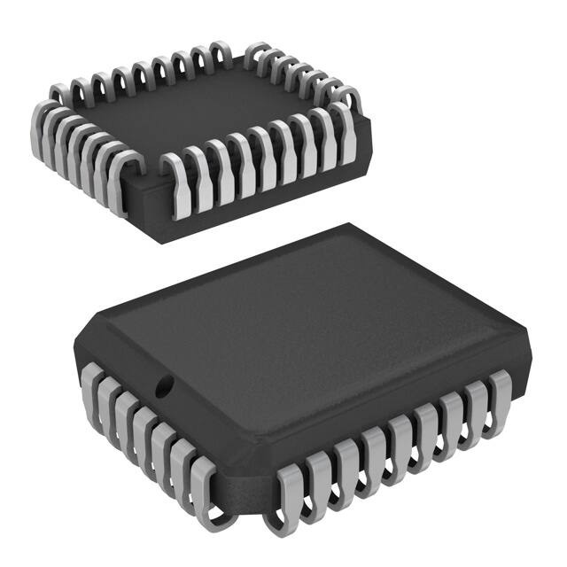
Package Diagram
32-Lead Plastic Leaded Chip Carrier J65 32-Lead Pb-Free Plastic Leaded Chip Carrier J65
51-85002-*B
Deep Sync is a trademark of Cypress Semiconductor. All product and company names mentioned in this document are the trademarks of their respective holders.
Document #: 38-06013 Rev. *B
Page 15 of 16
© Cypress Semiconductor Corporation, 2005. The information contained herein is subject to change without notice. Cypress Semiconductor Corporation assumes no responsibility for the use of any circuitry other than circuitry embodied in a Cypress product. Nor does it convey or imply any license under patent or other rights. Cypress products are not warranted nor intended to be used for medical, life support, life saving, critical control or safety applications, unless pursuant to an express written agreement with Cypress. Furthermore, Cypress does not authorize its products for use as critical components in life-support systems where a malfunction or failure may reasonably be expected to result in significant injury to the user. The inclusion of Cypress products in life-support systems application implies that the manufacturer assumes all risk of such use and in doing so indemnifies Cypress against all charges.
�CY7C4261V/CY7C4271V CY7C4281V/CY7C4291V
Document History Page
Document Title: CY7C4261V/CY7C4271V/CY7C4281V/CY7C4291V 16K/32K/64K/128K/X9 Low-Voltage Deep Sync FIFO Document Number: 38-06013 REV. ** *A *B ECN NO. Issue Date 106474 127858 386127 09/15/01 09/04/03 See ECN Orig. of Change SZV FSG ESH Description of Change Changed Spec number from 38-00656 to 38-06013 Changed: tSKEW2 to tSKEW1 in Switching Waveforms “Empty Flag Timing” diagram Fixed flag timing diagram in Switching Waveforms section Added Pb-Free logo to top of front page Added CY7C4291V-15JXC, CY7C91V-10JXC, CY7C4281V-10JXC, CY7C4271V-10JXC, CY7C4261V-10JXC, CY7C4261V-15JXC to ordering information.
Document #: 38-06013 Rev. *B
Page 16 of 16
�


 工商网监
湘ICP备2023018690号
工商网监
湘ICP备2023018690号
