CYV15G0104EQ
Multi Rate Video Cable Equalizer
Features
Functional Description
■
Multi rate adaptive equalization
■
Operates from 143 to 1485 Mbps serial data rate
■
SMPTE 292M, SMPTE 344M, and SMPTE 259M compliant
■
Supports DVB-ASI at 270 Mbps
■
Maximum cable length adjustment for HD-SDI and SD-SDI
data rates
The CYV15G0104EQ is a multi rate adaptive equalizer designed
to equalize and restore signals received over 75Ω coaxial cable.
The equalizer meets SMPTE 292M, SMPTE 344M, and SMPTE
259M data rates. The CYV15G0104EQ is optimized to equalize
up to 350m of Canare L-5CFB and Belden 1694A coaxial cable
at 270 Mbps and typically up to 200m of Canare L-5CFB and
Belden 1694A coaxial cable at 1.485 Gbps. The
CYV15G0104EQ connects seamlessly to the HOTLink II family
of transceiver devices.
■
Carrier detect and mute functionality for HD-SDI and SD-SDI
data rates
■
Equalizer bypass mode
■
Seamless connection with HOTLink II™ family
■
Equalizes up to 350m of Belden 1694A and Canare L-5CFB
coaxial cable at 270 Mbps
■
Typically equalizes up to 200m of Belden 1694A and Canare
L-5CFB coaxial cable at 1.485 Gbps
■
Low power: 160 mW at 3.3V
■
Single 3.3V supply
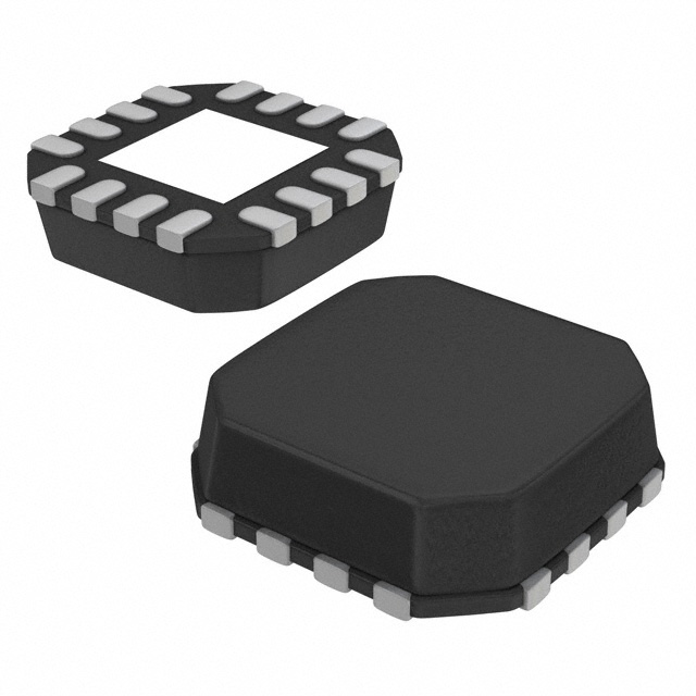
■
16-pin Quad Flat No Lead (QFN) package
■
0.18 μm CMOS technology
■
Pb-free and RoHS compliant
■
Pin compatible to existing QFN equalizer devices
■
Uses Cypress CLEANLink™ technology
The CYV15G0104EQ has DC restoration to compensate for the
DC content of the SMPTE pathological patterns. The maximum
cable length adjust (MCLADJ) sets the approximate maximum
cable length to equalize at SD and HD data rates. The
CYV15G0104EQ’s differential serial outputs (SDO, SDO) mute,
when the approximate cable length set by MCLADJ is reached,
and carrier detect (CD) is tied to MUTE. MUTE pin controls
muting the outputs of the equalizer at HD and SD data rates.
Power consumption is typically 160 mW at 3.3V.
Equalizer System Connection Diagram
HOTLink II
Serializer
Cable
Driver
Cypress Semiconductor Corporation
Document Number: 001-07425 Rev. **
•
CYV15G0104EQ
Multi Rate
Cable
Equalizer
Serial Links
Copper Cable
Connections
198 Champion Court
•
HOTLink II
Deserializer
San Jose, CA 95134-1709
•
408-943-2600
Revised October 25, 2007
[+] Feedback
�CYV15G0104EQ
Equalizer Block Diagram
CYV15G0104EQ Multi-Rate Video Cable Equalizer Block Diagram
CYV15G0104EQ Multi-Rate Video Cable Equalizer Block Diagram
MCLADJ
Cable Length Analog
Adjustor and Mute
Threshold Block
Carrier Detect and
Mute Control Block
MUTE
CD
DC Restore
BYPASS
SDI, SDI
Equalizer
Differential Output
SDO, SDO
Pinouts
SDI
3
GND
4
Document Number: 001-07425 Rev. **
CD
MUTE
VCC
13
CYV15G0104EQ
(Marked CY21EQ
On Package)
5
6
7
8
MCLADJ
2
14
BYPASS
SDI
15
AGC
1
16
AGC
GND
VCC
Figure 1. Pin Diagram - 16 Pin QFN (Top View)
12
GND
11
SDO
10
SDO
9
GND
Center Pad
(bottom of package)
Page 2 of 9
[+] Feedback
�CYV15G0104EQ
Table 1. Pin Descriptions - CYV15G0104EQ Single Channel Cable Equalizer
Name
IO Characteristics
Signal Description
Control Signals
MUTE
LVTTL Input
Mute.
When the MUTE pin is set LOW, the equalizer’s differential serial outputs are not muted.
When the MUTE pin is set HIGH, the equalizer’s differential serial outputs are muted.
BYPASS setting is ignored when MUTE is HIGH.
Connecting CD to MUTE pin enables automatic muting of the equalizer upon loss of signal.
Do not leave unused MUTE pin floating. Always drive it to a known state.
CD
LVTTL Output
Carrier Detect.
When the incoming data stream is present and maximum cable length does not exceed
that set by MCLADJ, CD outputs a voltage less than 0.8V.
When the incoming data stream is not present or maximum cable length exceeds that set
by MCLADJ, CD outputs a voltage greater than 2.8V.
Connecting CD to MUTE pin enables automatic muting of the equalizer upon loss of signal.
MCLADJ
Analog Input
Maximum Cable Length Adjust.
The maximum equalized cable length is set by the voltage applied to the MCLADJ input.
When the maximum cable length set by MCLADJ is reached, the CD indicator is
deasserted.
If MCLADJ functionality is not needed, this pin should be left floating or tied to ground to
allow maximum equalized cable length.
MCLADJ works at both SD and HD data rates.
BYPASS
LVTTL Input
Equalizer Bypass. When BYPASS is set HIGH, the signal presented at the equalizer’s
differential serial inputs (SDI, SDI) is routed to the equalizer’s differential serial outputs
(SDO, SDO) without equalizing.
When BYPASS is set LOW, the incoming video data stream is equalized and presented
at the equalizer‘s serial differential outputs (SDO, SDO).
When MUTE pin is set HIGH, BYPASS setting is ignored and the serial outputs are muted.
AGC, AGC
Analog
Automatic Gain Control. Place a capacitor of 1 μF between the AGC and AGC pins.
SDO, SDO
Differential
Output
Differential Serial Outputs. The equalized serial video data stream is presented at the
SDO/SDO differential serial CML output.
SDI, SDI
Differential
Input
Differential Serial Inputs. SDI/SDI accepts either a single-ended or differential serial
video data stream over 75Ω coaxial cable.
VCC
Power
Power Supply for Device. Connect to +3.3V DC.
GND
Gnd
Connect to Ground.
Center Pad
–
Connect to PCB Ground for Maximum Thermal Dissipation.
Power
Document Number: 001-07425 Rev. **
Page 3 of 9
[+] Feedback
�CYV15G0104EQ
Equalizer Operation
MUTE
The CYV15G0104EQ is a high speed adaptive cable equalizer
designed to equalize standard definition (SD) and high definition
(HD) serial digital interface (SDI) video data streams..The
CYV15G0104EQ equalizer is optimized to equalize up to 350m
of Belden 1694A cable and Canare L-5CFB cable at 270 Mbps
and typically up to 200m of Belden 1694A cable and Canare
L-5CFB cable at 1.485 Gbps. The CYV15G0104EQ equalizer
contains one power supply and typically consumes 160 mW
power at 3.3V. The multi rate equalizer meets the SMPTE 259M,
SMPTE 292M, SMPTE 344M, and DVB-ASI video standards. It
meets all pathological requirements for SMPTE 292M as defined
by RP198 and for SMPTE 259M as defined by RP178. The
CYV15G0104EQ multi rate cable equalizer operates from 143
Mbps to 1.485 Gbps serial data rate.
MUTE is an input pin that controls the muting of the equalizer’s
output. MUTE operates for both HD and SD data rates.
If MUTE is set LOW, the equalizer serial outputs are not muted.
If MUTE is set HIGH, then the equalizer serial outputs are muted.
When MUTE is active, BYPASS setting is also ignored.
Connecting CD to MUTE pin enables automatic muting of the
equalizer upon loss of signal.
Do not leave the MUTE pin floating. Always drive it to a known
state.
Carrier Detect (CD)
Carrier Detect is an active LOW output pin that indicates the
presence of a valid incoming data signal. When the incoming
data signal is present, and maximum cable length does not
exceed that set by MCLADJ, CD outputs a voltage less than
0.8V.
The CYV15G0104EQ equalizer has multiple variable gain equalization stages that reverse the attenuation effects of the cable.
This equalization is achieved by separate regulation of the lower
and higher frequency components in the signal to give a clean
output eye diagram. The CYV15G0104EQ has DC restoration to
compensate for the DC content of the SMPTE pathological
patterns.
When the incoming data stream is not present, or maximum
cable length exceeds that set by MCLADJ, CD outputs a voltage
greater than 2.8V.
SDI, SDI
Connecting CD to MUTE pin enables automatic muting of the
equalizer upon loss of signal.
CYV15G0104EQ accepts single-ended or differential serial
video data streams over 75Ω coaxial cable. It is recommended
to AC couple the SDI, SDI inputs as they are internally biased to
1.2V.
BYPASS
SDO, SDO
The CYV15G0104EQ has differential serial output interface
drivers that use Current Mode Logic (CML) drivers to provide
source matching for the transmission line. These outputs are
either AC coupled or DC coupled to HOTLink II receivers.
MCLADJ
Maximum Cable Length Adjust (MCLADJ) sets the approximate
maximum amount of cable to be equalized. When the maximum
cable length set by MCLADJ is reached, the CD pin is
deasserted. To enable automatic muting of the device upon loss
of signal, CD should be tied directly to MUTE. MCLADJ works at
SD and HD data rates.
The CYV15G0104EQ has a bypass mode that enables the user
to bypass the equalizer’s equalization and DC restoration
functions. When BYPASS is set HIGH, the signal presented at
the equalizer’s differential serial inputs (SDI, SDI) is routed to the
equalizer’s differential serial outputs (SDO, SDO) without equalizing.
When BYPASS is set LOW, the incoming video data stream is
equalized and presented at the equalizer‘s differential serial
outputs (SDO, SDO).
AGC
Place a capacitor of 1 μF between the AGC and AGC pins of the
CYV15G0104EQ equalizer
Figure 2 on page 7 illustrates the voltage required at MCLADJ
input to equalize various Belden 1694A cable lengths. If
MCLADJ functionality is not required, this pin should be left
floating or tied to ground to enable maximum equalized cable
length.
Document Number: 001-07425 Rev. **
Page 4 of 9
[+] Feedback
�CYV15G0104EQ
Maximum Ratings
Power Up Requirements
Exceeding maximum ratings may shorten the useful life of the
device. These user guidelines are not tested.
The CYV15G0104EQ contains one power supply. The voltage
on any input or IO pin must not exceed the power pin during
power up.
Storage Temperature .................................. –65°C to +150°C
Ambient Temperature with
Power Applied ............................................ –55°C to +125°C
Operating Range
Supply Voltage to Ground Potential................–0.5V to +3.8V
Range
Ambient
Temperature
DC Voltage Applied to Outputs
in High Z State ....................................... –0.5V to VCC + 0.5V
VCC
Commercial
0°C to +70°C
+3.3V ±5%
DC Input Voltage ..................................... –0.5V to VCC+0.5V
Electro Static Discharge (ESD) HBM....................... > 2000 V
(JEDEC EIA/JESD-A114A)
Latch Up Current .................................................... > 200 mA
DC Electrical Characteristics
Parameter
Description
Min
Typ
Max
Unit
–
3.135
3.3
3.465
V
–
125
160
190
mW
–
38
48
60
mA
Load = 50Ω
–
VCC – ΔVSDO/2
= 2.9
–
V
Input Common Mode Voltage[1]
(Bypass = High)
–
1
1.4
V
Input Common Mode Voltage[1]
(Bypass = Low)
–
0
2.9
V
Floating MCLADJ DC Voltage[1]
–
Supply
Voltage[1]
Power
Consumption[2]
IS
Supply
Current[1]
VCMOUT
Output Common Mode Voltage[1]
VCMIN
VCC
PD
–
–
VCD(OH)
MCLADJ
Range[2]
CD Output
Voltage[1]
VCD(OL)
Test Conditions
1.3
–
0.4
0.72
Carrier Not Present
2.8
–
Carrier Present
VMUTE
MUTE Input Voltage Required to Force
Outputs to Mute[1]
Min to Mute
VMUTE
MUTE Input Voltage Required to Force
Active[1]
Max to Activate
1.02
V
–
–
V
–
0.8
V
–
V
1
V
2.5
–
V
–
Notes
1. Production test.
2. Calculated results from production test.
Document Number: 001-07425 Rev. **
Page 5 of 9
[+] Feedback
�CYV15G0104EQ
AC Electrical Characteristics
Parameter
Description
Test Conditions
[1]
Min
Typ
Max
Unit
–
–
Serial Input Data Rate
–
143
1485
Mbps
VSDI
Input Voltage Swing
Single-ended, at the transmitter,
HD data rate
500[5]
1200
mV
VSDI
Input Voltage Swing
Single-ended, at the transmitter,
SD data rate
500[6]
1200
mV
ΔVSDO
Output Voltage Swing[1]
Differentialp-p, 50Ω load
950
mV
–
–
Output Jitter for Various Cable
Lengths and Data Rates
700
[1]
270 Mbps
Belden 1694A: 0-350m
Canare L-5CFB: 0-350m
800 mV transmit amplitude
Equalizer pathological pattern
–
0.2
–
UI
1.485 Gbps
Belden 1694A: 0-140m
Canare L-5CFB: 0-140m
800 mV transmit amplitude
Equalizer pathological pattern
–
0.25[1]
–
UI
1.485 Gbps
Belden 1694A: 140-200m
Canare L-5CFB: 140-200m
800 mV transmit amplitude
Equalizer pathological pattern
–
0.3[7]
–
UI
Output Rise/Fall Time[3, 4]
20% - 80%, HD data rate
80
120
220
ps
Time[3, 4]
20% - 80%, SD data rate
80
120
350
ps
–
–
30
ps
–
20
–
ps
–
–
–
10
%
–
Output Rise/Fall
–
450
Mismatch in Rise/Fall Time[3, 4]
Distortion[3, 4]
–
Duty Cycle
–
Overshoot[3, 4]
–
HD color bar pattern
Loss[3]
–
Input Return
-15
–
–
dB
–
Input Resistance[3, 4]
Single-ended
–
2.5
–
kΩ
–
Input Capacitance[3, 4]
Single-ended
–
1
–
pF
–
Resistance[3, 4]
Single-ended
–
50
–
Ω
Output
Notes
3. Not tested. Based on characterization.
4. Not tested. Guaranteed by design simulations.
5. Based on characterization across temperature and voltage with 140m of Belden 1694A cable, transmitting SMPTE Equalizer Pathological Test Pattern.
6. Based on characterization across temperature and voltage with 350m of Belden 1694A cable, transmitting SMPTE Equalizer Pathological Test Pattern.
7. Based on characterization at TA = 25°C, VCC = 3.3V
Document Number: 001-07425 Rev. **
Page 6 of 9
[+] Feedback
�CYV15G0104EQ
Typical Performance Graphs
(Unless otherwise stated, VCC = 3.3V, TA = 25°C)
Figure 2. MCLADJ Input Voltage vs Belden 1694A Cable Length at SD-SDI and HD-SDI Data Rates
2.7
2.6
2.5
VOLTAGE (V)
2.4
2.3
2.2
2.1
2
1.9
1.8
1.7
0
50
100
150
200
250
300
350
C A B L E LE N G T H (m )
Typical Application Circuit
Figure 3. Interfacing CYV15G0104EQ to the HOTLink II SerDes
+3.3V
+3.3V
C10
9
R18
Z0
C YV15G 0101DXB
Document Number: 001-07425 Rev. **
CD
VCC
VCC
GND
8
7
SDI
GND
R16
3
4
BNC JACK
75Ω
1
2
75Ω
1μF
L2
C16
6.4nH
37.4Ω
R15
R14
75Ω
5
6
C11
MCLADJ
GND
SDI
SDO
1μF
C15
AGC
2 Z0
MUTE
11
10
GND
SDO
AGC
12
Z0
0.01μF
13 14 15 16
BYPASS
IN1FRAMCHAR
RFEN
RFMODE
DECMODE
RXCKSEL
RXMODE
RXRATE
C12
0.01μF
MCLADJ
RXLE
SDASEL
LPEN
INSEL
IN1+
+
LFI
RXD7
RXD6
RXD5
RXD4
RXD3
RXD2
RXD1
RXD0
RXOP
RXST2
RXST1
RXST0
RXCLK+
RXCLKRXCLKC+
CYV15G0104EQ
1μF
Page 7 of 9
[+] Feedback
�CYV15G0104EQ
Ordering Information
Ordering Code
Package
Marking
Package Name
CYV15G0104EQ-LXC
CY21EQ
LY16A
Operating
Range
Package Type
Pb-free 16-Pin QFN
0 to 70°C
Package Dimension
Figure 4. 16-Pin QFN Package LY16A
0.05
3.90
4.10
C
2.50
REF.
1.00 MAX.
0.05 MAX.
3.70
3.80
0.80 MAX.
PIN1 ID
0.20 R.
0.35±0.05
0.20 REF.
N
2.50
N
REF.
1
2
1.90
2.00
3.90
4.10
3.70
3.80
1
2
E-PAD
0.45
0.30-0.50
0.42±0.18
(4X)
0°-12°
C
SEATING
PLANE
0.65
1.90
2.00
TOP VIEW
SIDE VIEW
DIMENSION IN mm
MIN.
MAX.
REFERENCE JEDEC MO-220
PKG. WEIGHT 0.04gms
Document Number: 001-07425 Rev. **
PART #
BOTTOM VIEW
001-04468-*A
LF16A STANDARD PKG.
LY16A LEAD FREE PKG.
Page 8 of 9
[+] Feedback
�CYV15G0104EQ
Document History Page
Document Title: CYV15G0104EQ Multi Rate Video Cable Equalizer
Document Number: 001-07425
Rev.
Ecn No.
Issue Date
Orig. Of
Change
**
1396423
SEE ECN
UKK/AESA
Description Of Change
New datasheet
© Cypress Semiconductor Corporation, 2007. The information contained herein is subject to change without notice. Cypress Semiconductor Corporation assumes no responsibility for the use of any
circuitry other than circuitry embodied in a Cypress product. Nor does it convey or imply any license under patent or other rights. Cypress products are not warranted nor intended to be used for medical,
life support, life saving, critical control or safety applications, unless pursuant to an express written agreement with Cypress. Furthermore, Cypress does not authorize its products for use as critical
components in life-support systems where a malfunction or failure may reasonably be expected to result in significant injury to the user. The inclusion of Cypress products in life-support systems
application implies that the manufacturer assumes all risk of such use and in doing so indemnifies Cypress against all charges.
Any Source Code (software and/or firmware) is owned by Cypress Semiconductor Corporation (Cypress) and is protected by and subject to worldwide patent protection (United States and foreign),
United States copyright laws and international treaty provisions. Cypress hereby grants to licensee a personal, non-exclusive, non-transferable license to copy, use, modify, create derivative works of,
and compile the Cypress Source Code and derivative works for the sole purpose of creating custom software and or firmware in support of licensee product to be used only in conjunction with a Cypress
integrated circuit as specified in the applicable agreement. Any reproduction, modification, translation, compilation, or representation of this Source Code except as specified above is prohibited without
the express written permission of Cypress.
Disclaimer: CYPRESS MAKES NO WARRANTY OF ANY KIND, EXPRESS OR IMPLIED, WITH REGARD TO THIS MATERIAL, INCLUDING, BUT NOT LIMITED TO, THE IMPLIED WARRANTIES
OF MERCHANTABILITY AND FITNESS FOR A PARTICULAR PURPOSE. Cypress reserves the right to make changes without further notice to the materials described herein. Cypress does not
assume any liability arising out of the application or use of any product or circuit described herein. Cypress does not authorize its products for use as critical components in life-support systems where
a malfunction or failure may reasonably be expected to result in significant injury to the user. The inclusion of Cypress’ product in a life-support systems application implies that the manufacturer
assumes all risk of such use and in doing so indemnifies Cypress against all charges.
Use may be limited by and subject to the applicable Cypress software license agreement.
Document Number: 001-07425 Rev. **
Revised October 25, 2007
Page 9 of 9
PSoC Designer™, Programmable System-on-Chip™, and PSoC Express™ are trademarks and PSoC® is a registered trademark of Cypress Semiconductor Corp. All other trademarks or registered
trademarks referenced herein are property of the respective corporations. Purchase of I2C components from Cypress or one of its sublicensed Associated Companies conveys a license under the
Philips I2C Patent Rights to use these components in an I2C system, provided that the system conforms to the I2C Standard Specification as defined by Philips. HOTLink is a registered trademark and
HOTLink II and CLEANLink are trademarks of Cypress Semiconductor. All other trademarks or registered trademarks referenced herein are property of the respective corporations. All products and
company names mentioned in this document may be the trademarks of their respective holders.
[+] Feedback
�


 工商网监
湘ICP备2023018690号
工商网监
湘ICP备2023018690号
