The following document contains information on Cypress products.
�MB91580L Series
32-bit Microcontroller
FR Family FR81S
MB91F585LA/F585LB/F585LC/F585LD/
MB91F586LA/F586LB/F586LC/F586LD/
MB91F587LA/F587LB/F587LC/F587LD
Data Sheet (Full Production)
Notice to Readers: This document states the current technical specifications regarding the Spansion
product(s) described herein. Spansion Inc. deems the products to have been in sufficient production volume
such that subsequent versions of this document are not expected to change. However, typographical or
specification corrections, or modifications to the valid combinations offered may occur.
Publication Number MB91F587LA_DS705-00012
CONFIDENTIAL
Revision 2.0
Issue Date August 22, 2014
�D a t a S h e e t
Notice On Data Sheet Designations
Spansion Inc. issues data sheets with Advance Information or Preliminary designations to
advise readers of product information or intended specifications throughout the product life
cycle, including development, qualification, initial production, and full production. In all cases,
however, readers are encouraged to verify that they have the latest information before
finalizing their design. The following descriptions of Spansion data sheet designations are
presented here to highlight their presence and definitions.
Advance Information
The Advance Information designation indicates that Spansion Inc. is developing one or more
specific products, but has not committed any design to production. Information presented in
a document with this designation is likely to change, and in some cases, development on the
product may discontinue. Spansion Inc. therefore places the following conditions upon
Advance Information content:
“This document contains information on one or more products under development
at Spansion Inc. The information is intended to help you evaluate this product. Do
not design in this product without contacting the factory. Spansion Inc. reserves the
right to change or discontinue work on this proposed product without notice.”
Preliminary
The Preliminary designation indicates that the product development has progressed such
that a commitment to production has taken place. This designation covers several aspects of
the product life cycle, including product qualification, initial production, and the subsequent
phases in the manufacturing process that occur before full production is achieved. Changes
to the technical specifications presented in a Preliminary document should be expected
while keeping these aspects of production under consideration. Spansion places the
following conditions upon Preliminary content:
“This document states the current technical specifications regarding the Spansion
product(s) described herein. The Preliminary status of this document indicates that
product qualification has been completed, and that initial production has begun.
Due to the phases of the manufacturing process that require maintaining efficiency
and quality, this document may be revised by subsequent versions or modifications
due to changes in technical specifications.”
Combination
Some data sheets contain a combination of products with different designations (Advance
Information, Preliminary, or Full Production). This type of document distinguishes these
products and their designations wherever necessary, typically on the first page, the ordering
information page, and pages with the DC Characteristics table and the AC Erase and
Program table (in the table notes). The disclaimer on the first page refers the reader to the
notice on this page.
Full Production (No Designation on Document)
When a product has been in production for a period of time such that no changes or only
nominal changes are expected, the Preliminary designation is removed from the data sheet.
Nominal changes may include those affecting the number of ordering part numbers available,
such as the addition or deletion of a speed option, temperature range, package type, or VIO
range. Changes may also include those needed to clarify a description or to correct a
typographical error or incorrect specification. Spansion Inc. applies the following conditions
to documents in this category:
“This document states the current technical specifications regarding the Spansion
product(s) described herein. Spansion Inc. deems the products to have been in
sufficient production volume such that subsequent versions of this document are
not expected to change. However, typographical or specification corrections, or
modifications to the valid combinations offered may occur.”
Questions regarding these document designations may be directed to your local sales office.
MB91F587LA_DS705-00012-2v0-E, August 22, 2014
CONFIDENTIAL
�MB91580L Series
32-bit Microcontroller
FR Family FR81S
MB91F585LA/F585LB/F585LC/F585LD/
MB91F586LA/F586LB/F586LC/F586LD/
MB91F587LA/F587LB/F587LC/F587LD
Data Sheet (Full Production)
DESCRIPTION
This series has Spansion 32-bit microcontrollers for automobile motor control. They use the FR81S CPU
that is compatible with the FR family.
Note: FR is a line of products of Spansion Inc.
FEATURES
• FR81S CPU Core
• 32-bit RISC, load/store architecture, pipeline 5-stage structure
• Maximum operating frequency: 128MHz (Source oscillation= 4.0MHz, 32 multiplied ( PLL clock
multiplication system) )
• General-purpose register: 32 bits, 16 sets
• 16-bit fixed length instructions (basic instructions), 1 instruction per cycle
• Instructions appropriate to embedded applications
• Memory-to-memory transfer instructions
• Bit manipulation instructions
• Barrel shift instructions
• High-level language support instructions
• Function entry/exit instructions
• Register content multi-load and store instructions
• Bit search instructions
Logical 1 detection, 0 detection, and change-point detection
• Branch instructions with delay slot
Overhead decrement during branch process
• Register interlock function
Easy assembler writing
• Built-in multiplier and instruction level support
• Signed 32-bit multiplication: 5 cycles
• Signed 16-bit multiplication: 3 cycles
Spansion provides information facilitating product development via the following website.
The website contains information useful for customers.
http://www.spansion.com/Support/microcontrollers/
Publication Number MB91F587LA_DS705-00012
Revision 2.0
Issue Date August 22, 2014
This document states the current technical specifications regarding the Spansion product(s) described herein. Spansion Inc. deems the products to have been in sufficient
production volume such that subsequent versions of this document are not expected to change. However, typographical or specification corrections, or modifications to the
valid combinations offered may occur.
CONFIDENTIAL
�D a t a S h e e t
• Interrupt (PC/PS saving)
6 cycles (16 priority levels)
• The Harvard architecture allows simultaneous execution of program and data access.
• Instruction compatibility with the FR family
• Built-in memory protection function (MPU)
• Eight protection areas can be specified commonly for instructions and data.
• Control access privilege in both privilege mode and user mode
• Built-in FPU (floating-point operation)
• IEEE754 compliant
• Floating-point register: 32 bits × 16 sets
• Peripheral Functions
• Clock generation (SSCG function is available)
• Main oscillation (4 to 20 MHz)
• PLL multiplication rate:1 to 32 times
• CR oscillation
• Oscillation frequency: 100kHz, with frequency accuracy ± 50% (pre-trimming)
• Trimming is enabled
• To be used as a count clock of hardware watchdog
• MB91F585LC/F586LC/F587LC/F585LD/F586LD/F587LD: Oscillation stop feature during stand-by
is not available
• MB91F585LA/F586LA/F587LA/F585LB/F586LB/F587LB: Oscillation stop feature during stand-by
is available
• Built-in program flash memory capacity
MB91F585L: 512+64 Kbytes
MB91F586L: 768+64 Kbytes
MB91F587L: 1024+64 Kbytes
• Built-in data flash (WorkFlash) 64 Kbytes
• Built-in RAM capacity
• Main RAM
MB91F585L: 48 Kbytes
MB91F586L: 64 Kbytes
MB91F587L: 96 Kbytes
• Backup RAM 8 Kbytes
• General-purpose ports:
MB91F585LA/F586LA/F587LA/F585LC/F586LC/F587LC 98 ports
MB91F585LB/F586LB/F587LB/F585LD/F586LD/F587LD 111 ports
• Including eight I2C pseudo open drain corresponding ports
• External bus interface (MB91F585LB/F586LB/F587LB/F585LD/F586LD/F587LD)
• Maximum operating frequency: 40MHz
• 22-bit address, 16-bit data
• DMA controller
• Up to 8 channels can be started simultaneously.
• 2 transfer factors (Internal peripheral request and software)
• External interrupt input: 8 channels
Level ("H" / "L") or edge detection (rising or falling) enabled
• Multi-function serial communication (built-in transmission/reception FIFO memory): 5 channels
< UART (Asynchronous serial interface) >
• Full-duplex double buffering system, 64-byte transmission FIFO memory, 64-byte reception FIFO
memory
• Parity or no parity is selectable.
• Built-in dedicated baud rate generator
• An external clock can be used as the transfer clock
• Parity, frame, and overrun error detection functions provided
• DMA transfer supported
2
CONFIDENTIAL
MB91F587LA_DS705-00012-2v0-E, August 22, 2014
�D a t a S h e e t
• Full-duplex double buffering system, 64-byte transmission FIFO memory, 64-byte reception FIFO
memory
• SPI supported; master and slave systems supported; 5 to 16, 20, 24, 32-bit data length can be set.
• Built-in dedicated baud rate generator (Master operation)
• An external clock can be entered. (Slave operation)
• Overrun error detection function is provided.
• Built-in chip selection function
• DMA transfer supported
• Full-duplex double buffering system, 64-byte transmission FIFO memory, 64-byte reception FIFO
memory
• LIN protocol revision2.1 supported.
• Master and slave systems supported
• Framing error and overrun error detection
• LIN synch break generation and detection; LIN synch delimiter generation
• Built-in dedicated baud rate generator
• An external clock can be adjusted by the reload counter.
• DMA transfer supported
< I2C >
• Supported for 4 channels: ch.0,ch.1,ch.3, and ch4.
• Full-duplex double buffering system, 64-byte transmission FIFO memory, 64-byte reception FIFO
memory
• Standard mode (Max. 100 kbps) / high-speed mode (Max. 400 kbps) supported
• DMA transfer supported (for transmission only)
• CAN controller (CAN): 3 channels
• Transfer speed: Up to 1Mbps
• 64-transmission/reception message buffering: 3 channels
• FlexRay controller: 1unit(ch.A/ch.B)
• FlexRay Specifications Version 2.1 supported
• Up to 128 message buffers
• 8K bytes of message RAM
• Variable length of message buffers
• Each message buffer can be allocated as a part of reception buffer, transmission buffer or reception
FIFO memory
• Host access to the message buffer via input and output buffers
• Filtering for slot counter, cycle counter and channels
• Maskable interrupts are supported
• PPG: 16 bits × 24 channels
• Reload timer: 16 bits × 4 channels
• A/D converter (successive approximation type)
• 12-bit resolution: 3units(24 channels)
• Conversion time: 1 µs
• Free-run timer: 16 bits × 6 channels (1 channel can be selected for input capture, and 1 channel for output
compare.)
• Input capture: 16 bits × 8 channels (linked to the free-run timer)
• Output compare: 16 bits × 12 channels (linked to the free-run timer)
• Waveform generator: 2 units (12 channels)
• R/D converter: 1 channel (MB91F585LA/F586LA/F587LA/F585LC/F586LC/F587LC)
• 10-bit D/A converter: 1 channel (MB91F585LB/F586LB/F587LB/F585LD/F586LD/F587LD)
• Calibration: The hardware watchdog for CR oscillation drive
The CR oscillation frequency can be trimmed.
August 22, 2014, MB91F587LA_DS705-00012-2v0-E
CONFIDENTIAL
3
�D a t a S h e e t
• Clock Supervisor
• Anomaly supervisory feature (by damaged quartz, etc.) of external main oscillation (4MHz)
• When anomaly is detected, clock is switched to CR.
• Up/ down counter: 2 channels
8/16-bit Up/ down counter
• Base timer: 2 channels
• 16-bit timer
• Any of four PWM/PPG/PWC/reload timer functions can be selected and used.
• As for the functions of PWC and reload timer, 2 channels of cascade mode can be used as 32-bit
timer..
• CRC generation
• Watchdog timer
• Hardware watchdog
• Software watchdog
• NMI
• Interrupt controller
• Interrupt request batch read
Multiple interrupts from peripherals can be read by a series of registers.
• I/O relocation
Change of pin position of peripheral functions
• Low-power consumption mode
• Sleep/Stop/Watch
• Stop (Power shut-off)/Watch (Power shut-off)
• Power-on reset
• Low-voltage detection reset (external low-voltage detection)
• Low-voltage detection reset (internal low-voltage detection)
• Device package: LQFP-144
• CMOS 90 nm technology
• Power supplies
• Single 5V power supply
• The voltage step-down circuit brings the 5.0V down to generate 1.2V internally
• I/O 5.0V
4
CONFIDENTIAL
MB91F587LA_DS705-00012-2v0-E, August 22, 2014
�D a t a S h e e t
PRODUCT LINEUP
MB91580L Series Product Lineup Comparison
• Memory size
Items
Flash memory capacity (program)
Flash memory capacity (work)
RAM capacity (main)
RAM capacity (backup)
• Function
Items
System clock
CR oscillation
Oscillation stop feature
during stand-by
External bus interface
DMA transfer
16-bit base timer
Free-run timer
Input capture
Output compare
Waveform generator
16-bit reload timer
PPG
External interrupt
A/D converter
R/D converter
D/A converter
Up/ down counter
Multi-function serial
interface
CAN
FlexRay
Software watchdog
Hardware watchdog
CRC generation
MB91F585LA
MB91F585LB
MB91F585LC
MB91F585LD
512+64 Kbytes
MB91F586LA
MB91F586LB
MB91F586LC
MB91F586LD
48 Kbytes
768+64 Kbytes
64 Kbytes
64 Kbytes
8 Kbytes
1024+64 Kbytes
96 Kbytes
MB91F585LA
MB91F586LA
MB91F587LA
MB91F585LB
MB91F586LB
MB91F587LB
MB91F585LC
MB91F586LC
MB91F587LC
MB91F585LD
MB91F586LD
MB91F587LD
Provided
Provided
Not provided
Not provided
On-chip PLL clock multiplication system
(Up to 32 times of multiplication)
Minimum instruction execution time: 7.81ns
(128MHz, source oscillation 4MHz × 32 times of multiplication)
Provided
Not provided
Provided
Not provided
Low-voltage detection reset
Address: 22 bits
Not provided
Data: 16 bits
8 channels
2 channels
6 channels
8 channels
12 channels
2 units (12 channels)
4 channels
24 channels
8 channels
3 units (24 channels)
Not provided
Provided
Provided
Not provided
2 channels
(External low-voltage
detection)
Device package
Debug interface
Provided
August 22, 2014, MB91F587LA_DS705-00012-2v0-E
Not provided
Provided
64 msb × 3 channels (ch.0/ch.1/ch.2)
128 msb × 1 unit (ch.A / ch.B)
Provided
Provided
1 channel
Provided
Low-voltage detection reset
Address: 22 bits
Data: 16 bits
5 channels
(Internal low-voltage
detection)
CONFIDENTIAL
MB91F587LA
MB91F587LB
MB91F587LC
MB91F587LD
LQFP-144
Built-in OCD (On Chip Debug Unit)
5
�D a t a S h e e t
MB91580M Series Product Lineup Comparison
• Memory size
Items
Flash memory capacity (program)
Flash memory capacity (work)
RAM capacity (main)
RAM capacity (backup)
• Function
Items
System clock
CR oscillation
Oscillation stop
feature during
stand-by
External bus interface
DMA transfer
16-bit base timer
Free-run timer
Input capture
Output compare
Waveform generator
16-bit reload timer
PPG
External interrupt
A/D converter
R/D converter
D/A converter
Up/ down counter
Multi-function serial
interface
CAN
FlexRay
Software watchdog
Hardware watchdog
CRC generation
Low-voltage detection reset
(Internal low-voltage
detection)
MB91F583MG
MB91F583MH
MB91F583MJ
MB91F583MK
MB91F584MG
MB91F584MH
MB91F584MJ
MB91F584MK
256+64 Kbytes
384+64 Kbytes
64 Kbytes
48 Kbytes
8 Kbytes
32 Kbytes
MB91F585MG
MB91F585MH
MB91F585MJ
MB91F585MK
512+64 Kbytes
48 Kbytes
MB91F583MG
MB91F584MG
MB91F585MG
MB91F583MH
MB91F584MH
MB91F585MH
MB91F583MJ
MB91F584MJ
MB91F585MJ
MB91F583MK
MB91F584MK
MB91F585MK
Provided
Provided
Not provided
Not provided
On-chip PLL clock multiplication system
(Up to 32 times of multiplication)
Minimum instruction execution time: 7.81ns
(128MHz, source oscillation 4MHz × 32 times of multiplication)
Provided
Not provided
8 channels
2 channels
6 channels
4 channels
7 channels
2 unit (7channels)
4 channels
6 channels
8 channels
3 units (23 channels)
Not provided
Provided
2 channels
4 channels
128msb × 1 unit
(ch.A / ch.B)
64msb × 2 channels (ch.0/ch.1)
128msb × 1 unit
Not provided
(ch.A / ch.B)
Provided
Provided
2 channels
Not provided
Provided
Low-voltage detection reset
(External low-voltage
Provided
detection)
Device package
LQFP-100
Debug interface
Built-in OCD (On Chip Debug Unit)
Note:
For details on the MB91580M series, see the "MB91580M/S Series HARDWARE MANUAL".
6
CONFIDENTIAL
MB91F587LA_DS705-00012-2v0-E, August 22, 2014
�D a t a S h e e t
MB91580S Series Product Lineup Comparison
• Memory size
Items
Flash memory capacity (program)
Flash memory capacity (work)
RAM capacity (main)
RAM capacity (backup)
• Function
Items
System clock
CR oscillation
Oscillation stop feature
during stand-by
External bus interface
DMA transfer
16-bit base timer
Free-run timer
Input capture
Output compare
Waveform generator
16-bit reload timer
PPG
External interrupt
A/D converter
R/D converter
D/A converter
Up/ down counter
Multi-function serial
interface
CAN
FlexRay
Software watchdog
Hardware watchdog
CRC generation
MB91F583SG
MB91F583SH
MB91F583SJ
MB91F583SK
256+64 Kbytes
MB91F584SG
MB91F584SH
MB91F584SJ
MB91F584SK
384+64 Kbytes
64 Kbytes
48 Kbytes
8 Kbytes
32 Kbytes
MB91F585SG
MB91F585SH
MB91F585SJ
MB91F585SK
512+64 Kbytes
48 Kbytes
MB91F583SG
MB91F584SG
MB91F585SG
MB91F583SH
MB91F584SH
MB91F585SH
MB91F583SJ
MB91F584SJ
MB91F585SJ
MB91F583SK
MB91F584SK
MB91F585SK
Provided
Provided
Not provided
Not provided
On-chip PLL clock multiplication system
(Up to 32 times of multiplication)
Minimum instruction execution time: 7.81ns
(128MHz, source oscillation 4MHz × 32 times of multiplication)
Provided
Not provided
8 channels
2 channels
6 channels
4 channels
7 channels
2 unit (7channels)
4 channels
6 channels
7 channels
3 units (17 channels)
Not provided
Provided
2 channels
2 channels
128msb × 1unit
(ch.A / ch.B)
Low-voltage detection reset
(Internal low-voltage
detection)
64msb × 1 channel (ch.0)
128msb × 1unit
Not provided
(ch.A / ch.B)
Provided
Provided
2 channels
Not provided
Provided
Low-voltage detection reset
(External low-voltage
Provided
detection)
Device package
LQFP-64
Debug interface
Built-in OCD (On Chip Debug Unit)
Note:
For details on the MB91580S series, see the "MB91580M/S Series HARDWARE MANUAL".
August 22, 2014, MB91F587LA_DS705-00012-2v0-E
CONFIDENTIAL
7
�D a t a S h e e t
PIN ASSIGNMENT
• LQFP-144 Pin Assignment
MB91F585LA/F586LA/F587LA/F585LC/F586LC/F587LC
144
143
142
141
140
139
138
137
136
135
134
133
132
131
130
129
128
127
126
125
124
123
122
121
120
119
118
117
116
115
114
113
112
111
110
109
VCC5
P014/TIOB1
P013/TIOA1
P012/TIOB0
P011/TIOA0
P010/RXDB
P007/TXDB
P006/SCS2/TXENB
P005/SCK2/RXDA
P004/SOT2/TXDA
P003/SIN2/TXENA/INT3
P002/SCK1
P001/SOT1
P000/SIN1/INT2
C
VSS
VCC5
P134/IN7/STOPWT/INT7/RX2
P133/ADTG2/TX2
P132/ADTG1/SCS1
P131/ADTG0
RSTX
P137/DTTI1
P136/DTTI0/MONCLK
VSS
X1
X0
MD1
MD0
P130/SCK0
P127/SOT0
P126/SIN0/INT6
P125/RTO11
P124/RTO10
DEBUGIF
VCC5
(TOP VIEW)
VSS
P015/TRG0
P016/TRG1
P017/TRG2
P020/TRG3/SIN3_1
P021/TRG4/SOT3_1
P022/TRG5/SCK3_1
P023/TIN0/SCS3_1
P024/TIN1/SIN4_1
P025/TIN2/SOT4_1
P026/TIN3/SCK4_1
P027/TOT0/SCS40_1
P030/TOT1/SCS41_1
P031/TOT2/SCS42_1
P032/TOT3/SCS43_1
P033
P034
VCC5
VSS
P035/AIN0/RDC_U
P036/BIN0/RDC_V
P037/ZIN0/RDC_W
P040/AIN1/RDC_A
P041/BIN1/RDC_B
P042/ZIN1/RDC_Z
RDC_ACT
MAG_OUT
MAG_PLUS
MAG_MINUS
COS_OUT
COS_MINUS
COS_PLUS
SIN_PLUS
SIN_MINUS
SIN_OUT
VCC5
1
2
3
4
5
6
7
8
9
10
11
12
13
14
15
16
17
18
19
20
21
22
23
24
25
26
27
28
29
30
31
32
33
34
35
36
108
107
106
105
104
103
102
101
100
99
98
97
96
95
94
93
92
91
90
89
88
87
86
85
84
83
82
81
80
79
78
77
76
75
74
73
LQFP-144
VSS
P123/RTO9
P122/RTO8
P121/RTO7/PPG23
P120/RTO6/PPG22
P117/RTO5/PPG21
P116/RTO4/PPG20
P115/RTO3/PPG19
P114/RTO2/PPG18
P113/RTO1/PPG17
P112/RTO0/PPG16
P111/RX1/INT1
P110/TX1
NMIX
VSS
VCC5
P107/AN23/PPG15
P106/AN22/PPG14
P105/AN21/PPG13
P104/AN20/PPG12
P103/AN19/PPG11
P102/AN18/PPG10
P101/AN17/PPG9
P100/AN16/PPG8
AVCC3
AVRH3
AVSS3/AVRL3
P097/IN5
P096/RX0/INT0
P095/TX0
P094/IN4
P093/IN3
P092/IN2
P091/IN1
P090/IN0
VSS
72
71
70
69
68
67
66
65
64
63
62
61
60
59
58
57
56
55
54
53
52
51
50
49
48
47
46
45
44
43
42
41
40
39
38
37
VCC5
P087/PPG7/AN15
P086/PPG6/AN14
P085/PPG5/AN13
P084/PPG4/AN12
P083/PPG3/AN11
P082/PPG2/AN10
P081/PPG1/AN9
P080/PPG0/AN8
AVSS2/AVRL2
AVRH2
P077/SCK3/AN7
P076/SOT3/AN6
P075/SIN3/INT4/AN5
P074/SCK4/AN4
P073/SOT4/AN3
P072/SIN4/INT5/AN2
P071/AN1
P070/AN0
AVSS1/AVRL1
AVRH1
P067/FRCK5
P066/FRCK4/SCS3
P065/FRCK3/SCS43
P064/FRCK2/SCS42
P063/FRCK1/SCS41
P062/FRCK0/SCS40
P061/IN6
P060/MM
AVSS0/AVRL0
AVRH0
AREF2
AVCC0
SIN_IN
COS_IN
VSS
(FTP-144P-M08)
8
CONFIDENTIAL
MB91F587LA_DS705-00012-2v0-E, August 22, 2014
�D a t a S h e e t
• MB91F585LB/F586LB/F587LB/F585LD/F586LD/F587LD
144
143
142
141
140
139
138
137
136
135
134
133
132
131
130
129
128
127
126
125
124
123
122
121
120
119
118
117
116
115
114
113
112
111
110
109
VCC5
P014/TIOB1/D28
P013/TIOA1/D27
P012/TIOB0/D26
P011/TIOA0/D25
P010/RXDB/D24
P007/TXDB/D23
P006/SCS2/TXENB/D22
P005/SCK2/RXDA/D21
P004/SOT2/TXDA/D20
P003/SIN2/TXENA/INT3/D19
P002/SCK1/D18
P001/SOT1/D17
P000/SIN1/INT2/D16
C
VSS
VCC5
P134/IN7/STOPWT/INT7/RX2
P133/ADTG2/TX2
P132/ADTG1/SCS1
P131/ADTG0
RSTX
P137/DTTI1
P136/DTTI0/MONCLK
VSS
X1
X0
MD1
MD0
P130/SCK0
P127/SOT0
P126/SIN0/INT6
P125/RTO11
P124/RTO10
DEBUGIF
VCC5
(TOP VIEW)
VSS
P015/TRG0/D29
P016/TRG1/D30
P017/TRG2/D31
P020/TRG3/SIN3_1/ASX
P021/TRG4/SOT3_1/CS0X
P022/TRG5/SCK3_1/CS1X
P023/TIN0/SCS3_1/RDX
P024/TIN1/SIN4_1/WR0X
P025/TIN2/SOT4_1/WR1X
P026/TIN3/SCK4_1/A00
P027/TOT0/SCS40_1/A01
P030/TOT1/SCS41_1/A02
P031/TOT2/SCS42_1/A03
P032/TOT3/SCS43_1/A04
P033/A05
P034/A06
VCC5
VSS
P035/AIN0/A07
P036/BIN0/A08
P037/ZIN0/A09
P040/AIN1/A10
P041/BIN1/A11
P042/ZIN1/A12
P043/A13
P044/DAOUT/A14
P045/A15
P046/A16
P047/A17
P050/A18
P051/A19
P052/A20
P053/A21
P054/SYSCLK
VCC5
1
2
3
4
5
6
7
8
9
10
11
12
13
14
15
16
17
18
19
20
21
22
23
24
25
26
27
28
29
30
31
32
33
34
35
36
LQFP-144
108
107
106
105
104
103
102
101
100
99
98
97
96
95
94
93
92
91
90
89
88
87
86
85
84
83
82
81
80
79
78
77
76
75
74
73
VSS
P123/RTO9
P122/RTO8
P121/RTO7/PPG23
P120/RTO6/PPG22
P117/RTO5/PPG21
P116/RTO4/PPG20
P115/RTO3/PPG19
P114/RTO2/PPG18
P113/RTO1/PPG17
P112/RTO0/PPG16
P111/RX1/INT1
P110/TX1
NMIX
VSS
VCC5
P107/AN23/PPG15
P106/AN22/PPG14
P105/AN21/PPG13
P104/AN20/PPG12
P103/AN19/PPG11
P102/AN18/PPG10
P101/AN17/PPG9
P100/AN16/PPG8
AVCC3
AVRH3
AVSS3/AVRL3
P097/IN5
P096/RX0/INT0
P095/TX0
P094/IN4
P093/IN3
P092/IN2
P091/IN1
P090/IN0
VSS
72
71
70
69
68
67
66
65
64
63
62
61
60
59
58
57
56
55
54
53
52
51
50
49
48
47
46
45
44
43
42
41
40
39
38
37
VCC5
P087/PPG7/AN15
P086/PPG6/AN14
P085/PPG5/AN13
P084/PPG4/AN12
P083/PPG3/AN11
P082/PPG2/AN10
P081/PPG1/AN9
P080/PPG0/AN8
AVSS2/AVRL2
AVRH2
P077/SCK3/AN7
P076/SOT3/AN6
P075/SIN3/INT4/AN5
P074/SCK4/AN4
P073/SOT4/AN3
P072/SIN4/INT5/AN2
P071/AN1
P070/AN0
AVSS1/AVRL1
AVRH1
P067/FRCK5
P066/FRCK4/SCS3
P065/FRCK3/SCS43
P064/FRCK2/SCS42
P063/FRCK1/SCS41
P062/FRCK0/SCS40
P061/IN6
P060/MM
AVSS0/AVRL0
AVRH0
P057/RDY
AVCC0
P056/CS3X
P055/CS2X
VSS
(FPT-144P-M08)
August 22, 2014, MB91F587LA_DS705-00012-2v0-E
CONFIDENTIAL
9
�D a t a S h e e t
PIN DESCRIPTION
• MB91F585LA/F586LA/F587LA/F585LC/F586LC/F587LC
Pin No.
Pin name
118
119
95
123
116
117
X0
X1
NMIX
RSTX
MD0
MD1
P000
INT2
SIN1
P001
131
132
133
134
135
136
137
138
139
140
141
142
143
2
3
10
CONFIDENTIAL
SOT1
P002
SCK1
P003
TXENA
INT3
SIN2
P004
TXDA
SOT2
P005
RXDA
SCK2
P006
TXENB
SCS2
P007
TXDB
P010
RXDB
P011
TIOA0
P012
TIOB0
P013
TIOA1
P014
TIOB1
P015
TRG0
P016
TRG1
I/O circuit
type*
A
B
B
C
C
E
K
K
O
N
N
N
N
N
D
D
D
D
D
D
Function
Main clock oscillation input pin
Main clock oscillation output pin
Interrupt input pin without mask
External reset input pin
Mode pin 0 (with high-voltage control)
Mode pin 1 (with high-voltage control)
General-purpose I/O port
INT2 external interrupt input pin
Multi-function serial ch.1 serial data input pin
General-purpose I/O port
Multi-function serial ch.1 serial data output pin/
I2C ch.1 serial data I/O pin (SDA)
General-purpose I/O port
Multi-function serial ch.1 clock I/O pin/
I2C ch.1 clock I/O pin (SCL)
General-purpose I/O port
FlexRay ch.A operation enable output pin
INT3 external interrupt input pin
Multi-function serial ch.2 serial data input pin
General-purpose I/O port
FlexRay ch.A data output pin
Multi-function serial ch.2 serial data output pin
General-purpose I/O port
FlexRay ch.A data input pin
Multi-function serial ch.2 clock I/O pin
General-purpose I/O port
FlexRay ch.B operation enable output pin
Multi-function serial ch2 serial chip select I/O pin
General-purpose I/O port
FlexRay ch.B data output pin
General-purpose I/O port
FlexRay ch.B data input pin
General-purpose I/O port
Base timer ch.0 TIOA I/O pin
General-purpose I/O port
Base timer ch.0 TIOB I/O pin
General-purpose I/O port
Base timer ch.1 TIOA I/O pin
General-purpose I/O port
Base timer ch.1 TIOB I/O pin
General-purpose I/O port
PPG ch.0 to ch.3 external trigger
General-purpose I/O port
PPG ch.4 to ch.7 external trigger
MB91F587LA_DS705-00012-2v0-E, August 22, 2014
�D a t a S h e e t
Pin No.
4
5
6
Pin name
P017
TRG2
P020
TRG3
SIN3_1
P021
TRG4
I/O circuit
type*
D
D
K
SOT3_1
7
P022
TRG5
K
SCK3_1
8
9
10
P023
TIN0
SCS3_1
P024
TIN1
SIN4_1
P025
TIN2
D
D
K
SOT4_1
11
P026
TIN3
K
SCK4_1
12
13
14
15
16
17
20
21
P027
TOT0
SCS40_1
P030
TOT1
SCS41_1
P031
TOT2
SCS42_1
P032
TOT3
SCS43_1
P033
P034
P035
AIN0
RDC_U
P036
BIN0
RDC_V
D
D
D
D
D
D
D
D
August 22, 2014, MB91F587LA_DS705-00012-2v0-E
CONFIDENTIAL
Function
General-purpose I/O port
PPG ch.8 to ch.11 external trigger
General-purpose I/O port
PPG ch.12 to ch.15 external trigger
Multi-function serial ch.3 serial data input pin (1)
General-purpose I/O port
PPG16 to PPG19 external trigger
Multi-function serial ch.3 serial data output pin (1)/
I2C ch.3 serial data I/O pin (1) (SDA)
General-purpose I/O port
PPG ch.20 to ch.23 external trigger
Multi-function serial ch.3 clock I/O pin (1)/
I2C ch.3 clock I/O pin (1) (SCL)
General-purpose I/O port
Reload timer ch.0 event input pin
Multi-function serial ch.3 serial chip select I/O pin (1)
General-purpose I/O port
Reload timer ch.1 event input pin
Multi-function serial ch.4 serial data input pin (1)
General-purpose I/O port
Reload timer ch.2 event input pin
Multi-function serial ch.4 serial data output pin (1)/
I2C ch.4 serial data I/O pin (1) (SDA)
General-purpose I/O port
Reload timer ch.3 event input pin
Multi-function serial ch.4 clock I/O pin (1)/
I2C ch.4 clock I/O pin (1) (SCL)
General-purpose I/O port
Reload timer ch.0 output pin
Multi-function serial ch.4 serial chip select 0 I/O pin (1)
General-purpose I/O port
Reload timer ch.1 output pin
Multi-function serial ch.4 serial chip select 1 output pin (1)
General-purpose I/O port
Reload timer ch.2 output pin
Multi-function serial ch.4 serial chip select 2 output pin (1)
General-purpose I/O port
Reload timer ch.3 output pin
Multi-function serial ch.4 serial chip select 3 output pin (1)
General-purpose I/O port
General-purpose I/O port
General-purpose I/O port
Up/ down counter ch.0 AIN input pin
RDC phase U output pin
General-purpose I/O port
Up/ down counter ch.0 BIN input pin
RDC phase V output pin
11
�D a t a S h e e t
Pin No.
22
23
24
25
26
27
28
29
30
31
32
33
34
35
38
39
41
44
45
46
47
48
49
50
51
12
CONFIDENTIAL
Pin name
P037
ZIN0
RDC_W
P040
AIN1
RDC_A
P041
BIN1
RDC_B
P042
ZIN1
RDC_Z
RDC_ACT
MAG_OUT
MAG_PLUS
MAG_MINUS
COS_OUT
COS_MINUS
COS_PLUS
SIN_PLUS
SIN_MINUS
SIN_OUT
COS_IN
SIN_IN
AREF2
P060
MM
P061
IN6
P062
FRCK0
SCS40
P063
FRCK1
SCS41
P064
FRCK2
SCS42
P065
FRCK3
SCS43
P066
FRCK4
SCS3
P067
FRCK5
I/O circuit
type*
D
D
D
D
J
I
H
H
I
H
H
H
H
I
H
H
I
D
D
D
D
D
D
D
D
Function
General-purpose I/O port
Up/ down counter ch.0 ZIN input pin
RDC phase W output pin
General-purpose I/O port
Up/ down counter ch.1 AIN input pin
RDC phase A output pin
General-purpose I/O port
Up/ down counter ch.1 BIN input pin
RDC phase B output pin
General-purpose I/O port
Up/ down counter ch.1 ZIN input pin
RDC phase Z output pin
RDC operation status output pin
RDC excitation signal output pin
RDC excitation external input pin +
RDC excitation external input pin RDC COS output pin
RDC COS input pin RDC COS input pin +
RDC SIN input pin +
RDC SIN input pin RDC SIN output pin
RDC COS coil earth leakage detection input pin
RDC SIN coil earth leakage detection input pin
RDC Aref output (AVcc0/2) pin
General-purpose I/O port
Clock supervisor main clock missing output pin
General-purpose I/O port
16-bit input capture ch.6 external pulse input pin
General-purpose I/O port
Free-run timer ch.0 external clock input pin
Multi-function serial ch.4 serial chip select 0 I/O pin
General-purpose I/O port
Free-run timer ch.1 external clock input pin
Multi-function serial ch.4 serial chip select 1 output pin
General-purpose I/O port
Free-run timer ch.2 external clock input pin
Multi-function serial ch.4 serial chip select 2 output pin
General-purpose I/O port
Free-run timer ch.3 external clock input pin
Multi-function serial ch.4 serial chip select 3 output pin
General-purpose I/O port
Free-run timer ch.4 external clock input pin
Multi-function serial ch.3 serial chip select I/O pin
General-purpose I/O port
Free-run timer ch.5 external clock input pin
MB91F587LA_DS705-00012-2v0-E, August 22, 2014
�D a t a S h e e t
Pin No.
54
55
56
57
Pin name
P070
AN0
P071
AN1
P072
AN2
SIN4
INT5
P073
AN3
I/O circuit
type*
F
F
G
M
SOT4
58
P074
AN4
M
SCK4
59
60
P075
AN5
SIN3
INT4
P076
AN6
G
M
SOT3
61
P077
AN7
M
SCK3
64
65
66
67
68
69
P080
AN8
PPG0
P081
AN9
PPG1
P082
AN10
PPG2
P083
AN11
PPG3
P084
AN12
PPG4
P085
AN13
PPG5
F
F
F
F
F
F
August 22, 2014, MB91F587LA_DS705-00012-2v0-E
CONFIDENTIAL
Function
General-purpose I/O port
ADC analog 0 input pin
General-purpose I/O port
ADC analog 1 input pin
General-purpose I/O port
ADC analog 2 input pin
Multi-function serial ch.4 serial data input pin
INT5 external interrupt input pin
General-purpose I/O port
ADC analog 3 input pin
Multi-function serial ch.4 serial data output pin/
I2C ch.4 serial data I/O pin (SDA)
General-purpose I/O port
ADC analog 4 input pin
Multi-function serial ch.4 clock I/O pin/
I2C ch.4 clock I/O pin (SCL)
General-purpose I/O port
ADC analog 5 input pin
Multi-function serial ch.3 serial data input pin
INT4 external interrupt input pin
General-purpose I/O port
ADC analog 6 input pin
Multi-function serial ch.3 serial data output pin/
I2C ch.3 serial data I/O pin (SDA)
General-purpose I/O port
ADC analog 7 input pin
Multi-function serial ch.3 clock I/O pin /
I2C ch.3 clock I/O pin (SCL)
General-purpose I/O port
ADC analog 8 input pin
PPG ch.0 output pin
General-purpose I/O port
ADC analog 9 input pin
PPG ch.1 output pin
General-purpose I/O port
ADC analog 10 input pin
PPG ch.2 output pin
General-purpose I/O port
ADC analog 11 input pin
PPG ch.3 output pin
General-purpose I/O port
ADC analog 12 input pin
PPG ch.4 output pin
General-purpose I/O port
ADC analog 13 input pin
PPG ch.5 output pin
13
�D a t a S h e e t
Pin No.
70
71
74
75
76
77
78
79
80
81
85
86
87
88
89
90
91
92
14
CONFIDENTIAL
Pin name
P086
AN14
PPG6
P087
AN15
PPG7
P090
IN0
P091
IN1
P092
IN2
P093
IN3
P094
IN4
P095
TX0
P096
RX0
INT0
P097
IN5
P100
PPG8
AN16
P101
PPG9
AN17
P102
PPG10
AN18
P103
PPG11
AN19
P104
PPG12
AN20
P105
PPG13
AN21
P106
PPG14
AN22
P107
PPG15
AN23
I/O circuit
type*
F
F
D
D
D
D
D
D
E
D
F
F
F
F
F
F
F
F
Function
General-purpose I/O port
ADC analog 14 input pin
PPG ch.6 output pin
General-purpose I/O port
ADC analog 15 input pin
PPG ch.7 output pin
General-purpose I/O port
16-bit input capture ch.0 external pulse input pin
General-purpose I/O port
16-bit input capture ch.1 external pulse input pin
General-purpose I/O port
16-bit input capture ch.2 external pulse input pin
General-purpose I/O port
16-bit input capture ch.3 external pulse input pin
General-purpose I/O port
16-bit input capture ch.4 external pulse input pin
General-purpose I/O port
CAN transmission data 0 output pin
General-purpose I/O port
CAN reception data 0 input pin
INT0 external interrupt input pin
General-purpose I/O port
16-bit input capture ch.5 external pulse input pin
General-purpose I/O port
PPG ch.8 output pin
ADC analog 16 input pin
General-purpose I/O port
PPG ch.9 output pin
ADC analog 17 input pin
General-purpose I/O port
PPG ch.10 output pin
ADC analog 18 input pin
General-purpose I/O port
PPG ch.11 output pin
ADC analog 19 input pin
General-purpose I/O port
PPG ch.12 output pin
ADC analog 20 input pin
General-purpose I/O port
PPG ch.13 output pin
ADC analog 21 input pin
General-purpose I/O port
PPG ch.14 output pin
ADC analog 22 input pin
General-purpose I/O port
PPG ch.15 output pin
ADC analog 23 input pin
MB91F587LA_DS705-00012-2v0-E, August 22, 2014
�D a t a S h e e t
Pin No.
96
97
98
99
100
101
102
103
104
105
106
107
111
112
113
114
115
Pin name
P110
TX1
P111
RX1
INT1
P112
RTO0
PPG16
P113
RTO1
PPG17
P114
RTO2
PPG18
P115
RTO3
PPG19
P116
RTO4
PPG20
P117
RTO5
PPG21
P120
RTO6
PPG22
P121
RTO7
PPG23
P122
RTO8
P123
RTO9
P124
RTO10
P125
RTO11
P126
SIN0
INT6
P127
SOT0
P130
SCK0
I/O circuit
type*
D
E
D
D
D
D
D
D
D
D
D
D
D
D
E
K
K
August 22, 2014, MB91F587LA_DS705-00012-2v0-E
CONFIDENTIAL
Function
General-purpose I/O port
CAN transmission data 1 output pin
General-purpose I/O port
CAN reception data 1 input pin
INT1 external interrupt input pin
General-purpose I/O port
Waveform generator ch.0 output pin
PPG ch.16 output pin
General-purpose I/O port
Waveform generator ch.1 output pin
PPG ch.17 output pin
General-purpose I/O port
Waveform generator ch.2 output pin
PPG ch.18 output pin
General-purpose I/O port
Waveform generator ch.3 output pin
PPG ch.19 output pin
General-purpose I/O port
Waveform generator ch.4 output pin
PPG ch.20 output pin
General-purpose I/O port
Waveform generator ch.5 output pin
PPG ch.21 output pin
General-purpose I/O port
Waveform generator ch.6 output pin
PPG ch.22 output pin
General-purpose I/O port
Waveform generator ch.7 output pin
PPG ch.23 output pin
General-purpose I/O port
Waveform generator ch.8 output pin
General-purpose I/O port
Waveform generator ch.9 output pin
General-purpose I/O port
Waveform generator ch.10 output pin
General-purpose I/O port
Waveform generator ch.11 output pin
General-purpose I/O port
Multi-function serial ch.0 serial data input pin
INT6 external interrupt input pin
General-purpose I/O port
Multi-function serial ch.0 serial data output pin/
I2C ch.0 serial data I/O pin (SDA)
General-purpose I/O port
Multi-function serial ch.0 clock I/O pin/
I2C ch.0 clock I/O pin (SCL)
15
�D a t a S h e e t
Pin No.
124
125
126
127
110
121
122
40
84
42
52
62
83
43
53
63
82
Pin name
P131
ADTG0
P132
ADTG1
SCS1
P133
ADTG2
TX2
P134
STOPWT
RX2
INT7
IN7
DEBUGIF
P136
DTTI0
MONCLK
P137
DTTI1
AVCC0
AVCC3
AVRH0
AVRH1
AVRH2
AVRH3
AVSS0
AVRL0
AVSS1
AVRL1
AVSS2
AVRL2
AVSS3
AVRL3
C
I/O circuit
type*
D
D
D
E
L
D
D
-
Function
General-purpose I/O port
A/D converter ch.0 to ch.7 external trigger input pin
General-purpose I/O port
A/D converter ch.8 to ch.15 external trigger input pin
Multi-function serial ch.1 serial chip select I/O pin
General-purpose I/O port
A/D converter ch.16 to ch.23 external trigger input pin
CAN transmission data 2 output pin
General-purpose I/O port
FlexRay Stopwatch input pin
CAN reception data 2 input pin
INT7 external interrupt input pin
16-bit input capture ch.7 external pulse input pin
DEBUG I/F pin
General-purpose I/O port
Waveform generator output stop signal input pin 0
Clock monitor output pin
General-purpose I/O port
Waveform generator output stop signal input pin 1
R/D converter power supply
A/D converter analog power supply
R/D converter upper limit reference voltage power supply
A/D converter upper limit reference voltage
A/D converter upper limit reference voltage
A/D converter upper limit reference voltage
R/D converter GND
R/D converter lower limit reference voltage
A/D converter GND
A/D converter lower limit reference voltage
A/D converter GND
A/D converter lower limit reference voltage
A/D converter GND
A/D converter lower limit reference voltage
External capacity connection output
130
18, 36,
93, 72,
VCC5
+5.0V power supply
109, 128,
144
1, 19, 37,
VSS
73, 94,
GND
108, 120,
129
*: For the I/O circuit types, see "■ I/O circuit type".
16
CONFIDENTIAL
MB91F587LA_DS705-00012-2v0-E, August 22, 2014
�D a t a S h e e t
• MB91F585LB/F586LB/F587LB/F585LD/F586LD/F587LD
I/O circuit
Pin No.
Pin name
Function
type*1
118
119
95
123
116
117
131
132
X0
X1
NMIX
RSTX
MD0
MD1
P000
D16
INT2
SIN1
P001
D17
A
B
B
C
C
E
K
SOT1
133
P002
D18
K
SCK1
134
135
136
137
138
139
140
P003
D19
TXENA
INT3
SIN2
P004
D20
TXDA
SOT2
P005
D21
RXDA
SCK2
P006
D22
TXENB
SCS2
P007
D23
TXDB
P010
D24
RXDB
P011
D25
TIOA0
O
N
N
N
N
N
D
August 22, 2014, MB91F587LA_DS705-00012-2v0-E
CONFIDENTIAL
Main clock oscillation input pin
Main clock oscillation output pin
Interrupt input pin without mask
External reset input pin
Mode pin 0 (with high-voltage control)
Mode pin 1 (with high-voltage control)
General-purpose I/O port
External bus data bit16 I/O pin
INT2 external interrupt input pin
Multi-function serial ch.1 serial data input pin
General-purpose I/O port
External bus data bit17 I/O pin
Multi-function serial ch.1 serial data output pin/
I2C ch.1 serial data I/O pin (SDA)
General-purpose I/O port
External bus data bit18 I/O pin
Multi-function serial ch.1 clock I/O pin /
I2C ch.1 clock I/O pin (SCL)
General-purpose I/O port
External bus data bit19 I/O pin
FlexRay ch.A operation enable output pin
INT3 external interrupt input pin
Multi-function serial ch.2 serial data input pin
General-purpose I/O port
External bus data bit20 I/O pin
FlexRay ch.A data output pin
Multi-function serial ch.2 serial data output pin
General-purpose I/O port
External bus data bit21 I/O pin
FlexRay ch.A data input pin
Multi-function serial ch.2 clock I/O pin
General-purpose I/O port
External bus data bit22 I/O pin
FlexRay ch.B operation enable output pin
Multi-function serial ch.2 serial chip select I/O pin
General-purpose I/O port
External bus data bit23 I/O pin
FlexRay ch.B data output pin
General-purpose I/O port
External bus data bit24 I/O pin
FlexRay ch.B data input pin
General-purpose I/O port
External bus data bit25 I/O pin
Base timer ch.0 TIOA I/O pin
17
�D a t a S h e e t
Pin No.
141
142
143
2
3
4
5
6
Pin name
P012
D26
TIOB0
P013
D27
TIOA1
P014
D28
TIOB1
P015
D29
TRG0
P016
D30
TRG1
P017
D31
TRG2
P020
ASX
TRG3
SIN3_1
P021
CS0X
TRG4
I/O circuit
type*1
D
D
D
D
D
D
D
K
SOT3_1
7
P022
CS1X
TRG5
K
SCK3_1
8
9
10
P023
RDX
TIN0
SCS3_1
P024
WR0X
TIN1
SIN4_1
P025
WR1X
TIN2
SOT4_1
18
CONFIDENTIAL
D
D
K
Function
General-purpose I/O port
External bus data bit26 I/O pin
Base timer ch.0 TIOB I/O pin
General-purpose I/O port
External bus data bit27 I/O pin
Base timer ch.1 TIOA I/O pin
General-purpose I/O port
External bus data bit28 I/O pin
Base timer ch.1 TIOB I/O pin
General-purpose I/O port
External bus data bit29 I/O pin
PPG ch.0 to ch.3 external trigger
General-purpose I/O port
External bus data bit30 I/O pin
PPG ch.4 to ch.7 external trigger
General-purpose I/O port
External bus data bit31 I/O pin
PPG ch.8 to ch.11 external trigger
General-purpose I/O port
External bus address strobe output pin
PPG ch.12 to ch.15 external trigger
Multi-function serial ch.3 serial data input pin (1)
General-purpose I/O port
External bus chip select 0 output pin
PPG16 to PPG19 external trigger
Multi-function serial ch.3 serial data output pin (1)/
I2C ch.3 serial data I/O pin (1) (SDA)
General-purpose I/O port
External bus chip select 1 output pin
PPG ch.20 to ch.23 external trigger
Multi-function serial ch.3 clock I/O pin (1)/
I2C ch.3 clock I/O pin (1) (SCL)
General-purpose I/O port
External bus read strobe output pin
Reload timer ch.0 event input pin
Multi-function serial ch.3 serial chip select I/O pin (1)
General-purpose I/O port
External bus write strobe 0 output pin
Reload timer ch.1 event input pin
Multi-function serial ch.4 serial data input pin (1)
General-purpose I/O port
External bus write strobe 1 output pin
Reload timer ch.2 event input pin
Multi-function serial ch.4 serial data output pin (1)/
I2C ch.4 serial data I/O pin (1) (SDA)
MB91F587LA_DS705-00012-2v0-E, August 22, 2014
�D a t a S h e e t
Pin No.
Pin name
11
P026
A00
TIN3
I/O circuit
type*1
K
SCK4_1
12
13
14
15
16
17
20
21
22
23
24
25
26
P027
A01
TOT0
SCS40_1
P030
A02
TOT1
SCS41_1
P031
A03
TOT2
SCS42_1
P032
A04
TOT3
SCS43_1
P033
A05
P034
A06
P035
A07
AIN0
P036
A08
BIN0
P037
A09
ZIN0
P040
A10
AIN1
P041
A11
BIN1
P042
A12
ZIN1
P043
A13
D
D
D
D
D
D
D
D
D
D
D
D
D
August 22, 2014, MB91F587LA_DS705-00012-2v0-E
CONFIDENTIAL
Function
General-purpose I/O port
External bus address bit0 output pin
Reload timer ch.3 event input pin
Multi-function serial ch.4 clock I/O pin (1)/
I2C ch.4 clock I/O pin (1) (SCL)
General-purpose I/O port
External bus address bit1 output pin
Reload timer ch.0 output pin
Multi-function serial ch.4 serial chip select 0 I/O pin (1)
General-purpose I/O port
External bus address bit2 output pin
Reload timer ch.1 output pin
Multi-function serial ch.4 serial chip select 1 output pin (1)
General-purpose I/O port
External bus address bit3 output pin
Reload timer ch.2 output pin
Multi-function serial ch.4 serial chip select 2 output pin (1)
General-purpose I/O port
External bus address bit4 output pin
Reload timer ch.3 output pin
Multi-function serial ch.4 serial chip select 3 output pin (1)
General-purpose I/O port
External bus address bit5 output pin
General-purpose I/O port
External bus address bit6 output pin
General-purpose I/O port
External bus address bit7 output pin
Up/ down counter ch.0 AIN input pin
General-purpose I/O port
External bus address bit8 output pin
Up/ down counter ch.0 BIN input pin
General-purpose I/O port
External bus address bit9 output pin
Up/ down counter ch.0 ZIN input pin
General-purpose I/O port
External bus address bit10 output pin
Up/ down counter ch.1 AIN input pin
General-purpose I/O port
External bus address bit11 output pin
Up/ down counter ch.1 BIN input pin
General-purpose I/O port
External bus address bit12 output pin
Up/ down counter ch.1 ZIN input pin
General-purpose I/O port
External bus address bit13 output pin
19
�D a t a S h e e t
Pin No.
27
28
29
30
31
32
33
34
35
38
39
41
44
45
46
47
48
49
50
51
20
CONFIDENTIAL
Pin name
P044
A14
DAOUT
P045
A15
P046
A16
P047
A17
P050
A18
P051
A19
P052
A20
P053
A21
P054
SYSCLK
P055
CS2X
P056
CS3X
P057
RDY
P060
MM
P061
IN6
P062
FRCK0
SCS40
P063
FRCK1
SCS41
P064
FRCK2
SCS42
P065
FRCK3
SCS43
P066
FRCK4
SCS3
P067
FRCK5
I/O circuit
type*1
P
D
D
D
D
D
D
D
D
D
D
D
D
D
D
D
D
D
D
D
Function
General-purpose I/O port
External bus address bit14 output pin
DAC analog output pin
General-purpose I/O port
External bus address bit15 output pin
General-purpose I/O port
External bus address bit16 output pin
General-purpose I/O port
External bus address bit17 output pin
General-purpose I/O port
External bus address bit18 output pin
General-purpose I/O port
External bus address bit19 output pin
General-purpose I/O port
External bus address bit20 output pin
General-purpose I/O port
External bus address bit21 output pin
General-purpose I/O port
External bus system clock output pin
General-purpose I/O port
External bus chip select 2 output pin
General-purpose I/O port
External bus chip select 3 output pin
General-purpose I/O port
External bus ready input pin
General-purpose I/O port
Clock supervisor main clock missing output pin
General-purpose I/O port
16-bit input capture ch.6 external pulse input pin
General-purpose I/O port
Free-run timer ch.0 external clock input pin
Multi-function serial ch.4 serial chip select 0 I/O pin
General-purpose I/O port
Free-run timer ch.1 external clock input pin
Multi-function serial ch.4 serial chip select 1 output pin
General-purpose I/O port
Free-run timer ch.2 external clock input pin
Multi-function serial ch.4 serial chip select 2 output pin
General-purpose I/O port
Free-run timer ch.3 external clock input pin
Multi-function serial ch.4 serial chip select 3 output pin
General-purpose I/O port
Free-run timer ch.4 external clock input pin
Multi-function serial ch.3 serial chip select I/O pin
General-purpose I/O port
Free-run timer ch.5 external clock input pin
MB91F587LA_DS705-00012-2v0-E, August 22, 2014
�D a t a S h e e t
Pin No.
54
55
56
57
Pin name
P070
AN0
P071
AN1
P072
AN2
SIN4
INT5
P073
AN3
I/O circuit
type*1
F
F
G
M
SOT4
58
P074
AN4
M
SCK4
59
60
P075
AN5
SIN3
INT4
P076
AN6
G
M
SOT3
61
P077
AN7
M
SCK3
64
65
66
67
68
69
P080
AN8
PPG0
P081
AN9
PPG1
P082
AN10
PPG2
P083
AN11
PPG3
P084
AN12
PPG4
P085
AN13
PPG5
F
F
F
F
F
F
August 22, 2014, MB91F587LA_DS705-00012-2v0-E
CONFIDENTIAL
Function
General-purpose I/O port
ADC analog 0 input pin
General-purpose I/O port
ADC analog 1 input pin
General-purpose I/O port
ADC analog 2 input pin
Multi-function serial ch.4 serial data input pin
INT5 external interrupt input pin
General-purpose I/O port
ADC analog 3 input pin
Multi-function serial ch.4 serial data output pin
I2C ch.4 serial data I/O pin (SDA)
General-purpose I/O port
ADC analog 4 input pin
Multi-function serial ch.4 clock I/O /
I2C ch.4 clock I/O pin (SCL)
General-purpose I/O port
ADC analog 5 input pin
Multi-function serial ch.3 serial data input pin
INT4 external interrupt input pin
General-purpose I/O port
ADC analog 6 input pin
Multi-function serial ch.3 serial data output pin /
I2C ch.3 serial data I/O pin (SDA)
General-purpose I/O port
ADC analog 7 input pin
Multi-function serial ch.3 clock I/O pin /
I2C ch.3 clock I/O pin (SCL)
General-purpose I/O port
ADC analog 8 input pin
PPG ch.0 output pin
General-purpose I/O port
ADC analog 9 input pin
PPG ch.1 output pin
General-purpose I/O port
ADC analog 10 input pin
PPG ch.2 output pin
General-purpose I/O port
ADC analog 11 input pin
PPG ch.3 output pin
General-purpose I/O port
ADC analog 12 input pin
PPG ch.4 output pin
General-purpose I/O port
ADC analog 13 input pin
PPG ch.5 output pin
21
�D a t a S h e e t
Pin No.
70
71
74
75
76
77
78
79
80
81
85
86
87
88
89
90
91
92
22
CONFIDENTIAL
Pin name
P086
AN14
PPG6
P087
AN15
PPG7
P090
IN0
P091
IN1
P092
IN2
P093
IN3
P094
IN4
P095
TX0
P096
RX0
INT0
P097
IN5
P100
PPG8
AN16
P101
PPG9
AN17
P102
PPG10
AN18
P103
PPG11
AN19
P104
PPG12
AN20
P105
PPG13
AN21
P106
PPG14
AN22
P107
PPG15
AN23
I/O circuit
type*1
F
F
D
D
D
D
D
D
E
D
F
F
F
F
F
F
F
F
Function
General-purpose I/O port
ADC analog 14 input pin
PPG ch.6 output pin
General-purpose I/O port
ADC analog 15 input pin
PPG ch.7 output pin
General-purpose I/O port
16-bit input capture ch.0 external pulse input pin
General-purpose I/O port
16-bit input capture ch.1 external pulse input pin
General-purpose I/O port
16-bit input capture ch.2 external pulse input pin
General-purpose I/O port
16-bit input capture ch.3 external pulse input pin
General-purpose I/O port
16-bit input capture ch.4 external pulse input pin
General-purpose I/O port
CAN transmission data 0 output pin
General-purpose I/O port
CAN reception data 0 input pin
INT0 external interrupt input pin
General-purpose I/O port
16-bit input capture ch.5 external pulse input pin
General-purpose I/O port
PPG ch.8 output pin
ADC analog 16 input pin
General-purpose I/O port
PPG ch.9 output pin
ADC analog 17 input pin
General-purpose I/O port
PPG ch.10 output pin
ADC analog 18 input pin
General-purpose I/O port
PPG ch.11 output pin
ADC analog 19 input pin
General-purpose I/O port
PPG ch.12 output pin
ADC analog 20 input pin
General-purpose I/O port
PPG ch.13 output pin
ADC analog 21 input pin
General-purpose I/O port
PPG ch.14 output pin
ADC analog 22 input pin
General-purpose I/O port
PPG ch.15 output pin
ADC analog 23 input pin
MB91F587LA_DS705-00012-2v0-E, August 22, 2014
�D a t a S h e e t
Pin No.
96
97
98
99
100
101
102
103
104
105
106
107
111
112
113
114
115
Pin name
P110
TX1
P111
RX1
INT1
P112
RTO0
PPG16
P113
RTO1
PPG17
P114
RTO2
PPG18
P115
RTO3
PPG19
P116
RTO4
PPG20
P117
RTO5
PPG21
P120
RTO6
PPG22
P121
RTO7
PPG23
P122
RTO8
P123
RTO9
P124
RTO10
P125
RTO11
P126
SIN0
INT6
P127
SOT0
P130
SCK0
I/O circuit
type*1
D
E
D
D
D
D
D
D
D
D
D
D
D
D
E
K
K
August 22, 2014, MB91F587LA_DS705-00012-2v0-E
CONFIDENTIAL
Function
General-purpose I/O port
CAN transmission data 1 output pin
General-purpose I/O port
CAN reception data 1 input pin
INT1 external interrupt input pin
General-purpose I/O port
Waveform generator ch.0 output pin
PPG ch.16 output pin
General-purpose I/O port
Waveform generator ch.1 output pin
PPG ch.17 output pin
General-purpose I/O port
Waveform generator ch.2 output pin
PPG ch.18 output pin
General-purpose I/O port
Waveform generator ch.3 output pin
PPG ch.19 output pin
General-purpose I/O port
Waveform generator ch.4 output pin
PPG ch.20 output pin
General-purpose I/O port
Waveform generator ch.5 output pin
PPG ch.21 output pin
General-purpose I/O port
Waveform generator ch.6 output pin
PPG ch.22 output pin
General-purpose I/O port
Waveform generator ch.7 output pin
PPG ch.23 output pin
General-purpose I/O port
Waveform generator ch.8 output pin
General-purpose I/O port
Waveform generator ch.9 output pin
General-purpose I/O port
Waveform generator ch.10 output pin
General-purpose I/O port
Waveform generator ch.11 output pin
General-purpose I/O port
Multi-function serial ch.0 serial data input pin
INT6 external interrupt input pin
General-purpose I/O port
Multi-function serial ch.0 serial data output pin/
I2C ch.0 serial data I/O pin (SDA)
General-purpose I/O port
Multi-function serial ch.0 clock I/O pin/
I2C ch.0 clock I/O pin (SCL)
23
�D a t a S h e e t
Pin No.
124
125
126
127
110
121
122
40
84
42
52
62
83
43
53
63
82
Pin name
P131
ADTG0
P132
ADTG1
SCS1
P133
ADTG2
TX2
P134
STOPWT
RX2
INT7
IN7
DEBUGIF
P136
DTTI0
MONCLK
P137
DTTI1
AVCC0
AVCC3
AVRH0
AVRH1
AVRH2
AVRH3
AVSS0
AVRL0
AVSS1
AVRL1
AVSS2
AVRL2
AVSS3
AVRL3
C
I/O circuit
type*1
D
D
D
E
L
D
D
-
Function
General-purpose I/O port
A/D converter ch.0 to ch.7 external trigger input pin
General-purpose I/O port
A/D converter ch.8 to ch.15 external trigger input pin
Multi-function serial ch.1 serial chip select I/O pin
General-purpose I/O port
A/D converter ch.16 to ch.23 external trigger input pin
CAN transmission data 2 output pin
General-purpose I/O port
FlexRay Stopwatch input pin
CAN reception data 2 input pin
INT7 external interrupt input pin
16-bit input capture ch.7 external pulse input pin
DEBUG I/F pin
General-purpose I/O port
Waveform generator output stop signal input pin 0
Clock monitor output pin
General-purpose I/O port
Waveform generator output stop signal input pin 1
*2
A/D converter analog power supply
*2
A/D converter upper limit reference voltage
A/D converter upper limit reference voltage
A/D converter upper limit reference voltage
*3
*3
A/D converter GND
A/D converter lower limit reference voltage
A/D converter GND
A/D converter lower limit reference voltage
A/D converter GND
A/D converter lower limit reference voltage
External capacity connection output pin
130
18, 36,
93, 72,
VCC5
+5.0V power supply
109, 128,
144
1, 19, 37,
73, 94,
VSS
GND
108, 120,
129
*1: For the I/O circuit types, see "■ I/O circuit type".
*2: The MB91F585LB/F586LB/F587LB/F585LD/F586LD/F587LD do not use this pin. Connect it with the
VCC5 pin.
*3: The MB91F585LB/F586LB/F587LB/F585LD/F586LD/F587LD do not use this pin. Connect it with the VSS
pin.
24
CONFIDENTIAL
MB91F587LA_DS705-00012-2v0-E, August 22, 2014
�D a t a S h e e t
I/O CIRCUIT TYPE
Type
A
Circuit
X1
Remarks
Clock input
Oscillation feedback resistor:
Approx. 1 MΩ
X0
Standby control signal
B
• CMOS hysteresis input
• With 50 kΩ pull-up resistor
Pull-up resistor
CMOS hysteresis input
C
Mode input
N-ch
N-ch
High withstand voltage mode
input
N-ch
High withstand voltage control
• Schmitt input
• With high withstand voltage
control
N-ch
D
Pull-up control
P-ch
P-ch
Digital output
N-ch
• General-purpose I/O port
• CMOS level output
IOH=-2/-5mA, IOL=2/5mA
• With 50kΩ pull-up resistor control
• CMOS hysteresis input
(0.7Vcc/0.3Vcc)
• Automotive input (0.8Vcc/0.5Vcc)
R
CMOS hysteresis input
Automotive input
Standby control
August 22, 2014, MB91F587LA_DS705-00012-2v0-E
CONFIDENTIAL
25
�D a t a S h e e t
Type
Circuit
E
Remarks
Pull-up control
P-ch
P-ch
Digital output
N-ch
• General-purpose I/O port
• CMOS level output
IOH=-2/-5mA, IOL=2/5mA
• With 50 kΩ pull-up resistor control
• CMOS hysteresis input
(0.7Vcc/0.3Vcc)
During standby, the input value
retains the previous value.
• Automotive input (0.8Vcc/0.5Vcc)
During standby, the input value
retains the previous value.
R
CMOS hysteresis input
Automotive input
Standby control
F
Pull-up control
P-ch
P-ch
Digital output
N-ch
• With analog input, general-purpose
I/O port
• CMOS level output
IOH=-2/-5mA, IOL=2/5mA
• With 50 kΩ pull-up resistor control
• CMOS hysteresis input
(0.7Vcc/0.3Vcc)
• Automotive input (0.8Vcc/0.5Vcc)
R
CMOS hysteresis input
Automotive input
Standby control
Analog input
26
CONFIDENTIAL
MB91F587LA_DS705-00012-2v0-E, August 22, 2014
�D a t a S h e e t
Type
Circuit
G
Remarks
Pull-up control
P-ch
P-ch
Digital output
N-ch
R
• With analog input, general-purpose
I/O port
• CMOS level output
IOH=-2/-5mA, IOL=2/5mA
• With 50 kΩ pull-up resistor control
• CMOS hysteresis input
(0.7Vcc/0.3Vcc)
During standby, the input value
retains the previous value.
• Automotive input (0.8Vcc/0.5Vcc)
During standby, the input value
retains the previous value.
CMOS hysteresis input
Automotive input
Standby control
Analog input
H*
Analog input
Analog input
I*
Analog output
Analog output
J*
CMOS level output
IOH=-2/-5mA, IOL=2/5mA
P-ch
Digital output
N-ch
K
Pull-up control
P-ch
P-ch
Digital output
N-ch
• With I2C, general-purpose I/O port
• CMOS level output
IOH=-3mA, IOL=3mA (at I2C
output)
IOH=-2/-5mA, IOL=2/5mA (other
than above)
• With 50 kΩ pull-up resistor control
• CMOS hysteresis input
(0.7Vcc/0.3Vcc)
• Automotive input (0.8Vcc/0.5Vcc)
R
CMOS hysteresis input
Automotive input
Standby control
August 22, 2014, MB91F587LA_DS705-00012-2v0-E
CONFIDENTIAL
27
�D a t a S h e e t
Type
Circuit
L
Remarks
Open drain I/O
Digital output
TTL schmitt input
M
Pull-up control
P-ch
P-ch
Digital output
N-ch
• With analog input, I2C,
general-purpose I/O port
• CMOS level output
IOH=-3mA, IOL=3mA (at I2C
output)
IOH=-2/-5mA, IOL=2/5mA (other
than above)
• With 50 kΩ pull-up resistor control
• CMOS hysteresis input
(0.7Vcc/0.3Vcc)
• Automotive input (0.8Vcc/0.5Vcc)
R
CMOS hysteresis input
Automotive input
Standby control
Analog input
N
Pull-up control
P-ch
P-ch
Digital output
N-ch
• With analog output,
general-purpose I/O port
• CMOS level output
IOH=-2/-4mA, IOL=2/4mA
• With 50 kΩ pull-up resistor control
• FlexRay input (0.7Vcc/0.3Vcc)
• Automotive input (0.8Vcc/0.5Vcc)
R
FlexRay input
Automotive input
Standby control
Analog output
28
CONFIDENTIAL
MB91F587LA_DS705-00012-2v0-E, August 22, 2014
�D a t a S h e e t
Type
Circuit
O
Remarks
Pull-up control
P-ch
P-ch
Digital output
N-ch
• With analog output,
general-purpose I/O port
• CMOS level output
IOH=-2/-4mA, IOL=2/4mA
• With 50 kΩ pull-up resistor control
• FlexRay input (0.7Vcc/0.3Vcc)
During standby, the input value
retains the previous value.
• Automotive input (0.8Vcc/0.5Vcc)
During standby, the input value
retains the previous value.
R
FlexRay input
Automotive input
Standby control
Analog output
P
Pull-up control
P-ch
P-ch
Digital output
N-ch
• With D/A converter output,
general-purpose I/O port
• CMOS level output
IOH=-2/-5mA, IOL=2/5mA
• With 50 kΩ pull-up resistor control
• CMOS hysteresis input
(0.7Vcc/0.3Vcc)
• Automotive input (0.8Vcc/0.5Vcc)
R
CMOS hysteresis input
Automotive input
Standby control
D/A converter output
*: MB91F585LA/F586LA/F587LA/F585LC/F586LC/F587LC only
August 22, 2014, MB91F587LA_DS705-00012-2v0-E
CONFIDENTIAL
29
�D a t a S h e e t
HANDLING PRECAUTIONS
Any semiconductor devices have inherently a certain rate of failure. The possibility of failure is greatly
affected by the conditions in which they are used (circuit conditions, environmental conditions, etc.). This
page describes precautions that must be observed to minimize the chance of failure and to obtain higher
reliability from your Spansion semiconductor devices.
1.
Precautions for Product Design
This section describes precautions when designing electronic equipment using semiconductor devices.
• Absolute Maximum Ratings
Semiconductor devices can be permanently damaged by application of stress (voltage, current, temperature,
etc.) in excess of certain established limits, called absolute maximum ratings. Do not exceed these ratings.
• Recommended Operating Conditions
Recommended operating conditions are normal operating ranges for the semiconductor device. All the
device's electrical characteristics are warranted when operated within these ranges.
Always use semiconductor devices within the recommended operating conditions. Operation outside these
ranges may adversely affect reliability and could result in device failure.
No warranty is made with respect to uses, operating conditions, or combinations not represented on the data
sheet. Users considering application outside the listed conditions are advised to contact their sales
representative beforehand.
• Processing and Protection of Pins
These precautions must be followed when handling the pins which connect semiconductor devices to power
supply and input/output functions.
(1) Preventing Over-Voltage and Over-Current Conditions
Exposure to voltage or current levels in excess of maximum ratings at any pin is likely to cause
deterioration within the device, and in extreme cases leads to permanent damage of the device. Try to
prevent such overvoltage or over-current conditions at the design stage.
(2) Protection of Output Pins
Shorting of output pins to supply pins or other output pins, or connection to large capacitance can
cause large current flows. Such conditions if present for extended periods of time can damage the
device.
Therefore, avoid this type of connection.
(3) Handling of Unused Input Pins
Unconnected input pins with very high impedance levels can adversely affect stability of operation.
Such pins should be connected through an appropriate resistance to a power supply pin or ground pin.
• Latch-up
Semiconductor devices are constructed by the formation of P-type and N-type areas on a substrate. When
subjected to abnormally high-voltages, internal parasitic PNPN junctions (called thyristor structures) may
be formed, causing large current levels in excess of several hundred mA to flow continuously at the power
supply pin. This condition is called latch-up.
CAUTION: The occurrence of latch-up not only causes loss of reliability in the semiconductor device, but
can cause injury or damage from high heat, smoke or flame. To prevent this from happening, do the
following:
(1) Be sure that voltages applied to pins do not exceed the absolute maximum ratings. This should
include attention to abnormal noise, surge levels, etc.
(2) Be sure that abnormal current flows do not occur during the power-on sequence.
Code: DS00-00004-1Ea
30
CONFIDENTIAL
MB91F587LA_DS705-00012-2v0-E, August 22, 2014
�D a t a S h e e t
• Observance of Safety Regulations and Standards
Most countries in the world have established standards and regulations regarding safety, protection from
electromagnetic interference, etc. Customers are requested to observe applicable regulations and standards
in the design of products.
• Fail-Safe Design
Any semiconductor devices have inherently a certain rate of failure. You must protect against injury,
damage or loss from such failures by incorporating safety design measures into your facility and equipment
such as redundancy, fire protection, and prevention of over-current levels and other abnormal operating
conditions.
• Precautions Related to Usage of Devices
Spansion semiconductor devices are intended for use in standard applications (computers, office automation
and other office equipment, industrial, communications, and measurement equipment, personal or
household devices, etc.).
CAUTION: Customers considering the use of our products in special applications where failure or
abnormal operation may directly affect human lives or cause physical injury or property damage, or where
extremely high levels of reliability are demanded (such as aerospace systems, atomic energy controls, sea
floor repeaters, vehicle operating controls, medical devices for life support, etc.) are requested to consult
with sales representatives before such use. The company will not be responsible for damages arising from
such use without prior approval.
2.
Precautions for Package Mounting
Package mounting may be either lead insertion type or surface mount type. In either case, for heat resistance
during soldering, you should only mount under Spansion's recommended conditions. For detailed
information about mount conditions, contact your sales representative.
• Lead Insertion Type
Mounting of lead insertion type packages onto printed circuit boards may be done by two methods: direct
soldering on the board, or mounting by using a socket.
Direct mounting onto boards normally involves processes for inserting leads into through-holes on the
board and using the flow soldering (wave soldering) method of applying liquid solder. In this case, the
soldering process usually causes leads to be subjected to thermal stress in excess of the absolute ratings for
storage temperature. Mounting processes should conform to Spansion recommended mounting conditions.
If socket mounting is used, differences in surface treatment of the socket contacts and IC lead surfaces can
lead to contact deterioration after long periods. For this reason it is recommended that the surface treatment
of socket contacts and IC leads be verified before mounting.
• Surface Mount Type
Surface mount packaging has longer and thinner leads than lead-insertion packaging, and therefore leads are
more easily deformed or bent. The use of packages with higher pin counts and narrower pin pitch results in
increased susceptibility to open connections caused by deformed pins, or shorting due to solder bridges.
You must use appropriate mounting techniques. Spansion Inc. recommends the solder reflow method, and
has established a ranking of mounting conditions for each product. Users are advised to mount packages in
accordance with Spansion ranking of recommended conditions.
August 22, 2014, MB91F587LA_DS705-00012-2v0-E
CONFIDENTIAL
31
�D a t a S h e e t
• Lead-Free Packaging
CAUTION: When ball grid array (BGA) packages with Sn-Ag-Cu balls are mounted using Sn-Pb eutectic
soldering, junction strength may be reduced under some conditions of use.
• Storage of Semiconductor Devices
Because plastic chip packages are formed from plastic resins, exposure to natural environmental conditions
will cause absorption of moisture. During mounting, the application of heat to a package that has absorbed
moisture can cause surfaces to peel, reducing moisture resistance and causing packages to crack. To prevent,
do the following:
(1) Avoid exposure to rapid temperature changes, which cause moisture to condense inside the product.
Store products in locations where temperature changes are slight.
(2) Use dry boxes for product storage. Products should be stored below 70% relative humidity, and at
temperatures between 5°C and 30°C.
When you open Dry Package that recommends humidity 40% to 70% relative humidity.
(3) When necessary, Spansion Inc. packages semiconductor devices in highly moisture-resistant
aluminum laminate bags, with a silica gel desiccant. Devices should be sealed in their aluminum
laminate bags for storage.
(4) Avoid storing packages where they are exposed to corrosive gases or high levels of dust.
• Baking
Packages that have absorbed moisture may be de-moisturized by baking (heat drying). Follow the Spansion
recommended conditions for baking.
Condition: 125°C/24 h
• Static Electricity
Because semiconductor devices are particularly susceptible to damage by static electricity, you must take
the following precautions:
(1) Maintain relative humidity in the working environment between 40% and 70%. Use of an apparatus
for ion generation may be needed to remove electricity.
(2) Electrically ground all conveyors, solder vessels, soldering irons and peripheral equipment.
(3) Eliminate static body electricity by the use of rings or bracelets connected to ground through high
resistance (on the level of 1 MΩ).
Wearing of conductive clothing and shoes, use of conductive floor mats and other measures to
minimize shock loads is recommended.
(4) Ground all fixtures and instruments, or protect with anti-static measures.
(5) Avoid the use of styrofoam or other highly static-prone materials for storage of completed board
assemblies.
32
CONFIDENTIAL
MB91F587LA_DS705-00012-2v0-E, August 22, 2014
�D a t a S h e e t
3.
Precautions for Use Environment
Reliability of semiconductor devices depends on ambient temperature and other conditions as described
above.
For reliable performance, do the following:
(1) Humidity
Prolonged use in high humidity can lead to leakage in devices as well as printed circuit boards. If high
humidity levels are anticipated, consider anti-humidity processing.
(2) Discharge of Static Electricity
When high-voltage charges exist close to semiconductor devices, discharges can cause abnormal
operation. In such cases, use anti-static measures or processing to prevent discharges.
(3) Corrosive Gases, Dust, or Oil
Exposure to corrosive gases or contact with dust or oil may lead to chemical reactions that will
adversely affect the device. If you use devices in such conditions, consider ways to prevent such
exposure or to protect the devices.
(4) Radiation, Including Cosmic Radiation
Most devices are not designed for environments involving exposure to radiation or cosmic radiation.
Users should provide shielding as appropriate.
(5) Smoke, Flame
CAUTION: Plastic molded devices are flammable, and therefore should not be used near combustible
substances. If devices begin to smoke or burn, there is danger of the release of toxic gases.
Customers considering the use of Spansion products in other special environmental conditions should
consult with sales representatives.
Please check the latest handling precautions at the following URL.
http://www.spansion.com/fjdocuments/fj/datasheet/e-ds/DS00-00004.pdf
August 22, 2014, MB91F587LA_DS705-00012-2v0-E
CONFIDENTIAL
33
�D a t a S h e e t
HANDLING DEVICES
The latch-up prevention and pin processing are explained below.
• For latch-up prevention
If a voltage higher than VCC or a voltage lower than VSS is applied to an I/O pin, or if a voltage exceeding
the ratings is applied between VCC and VSS pins, a latch-up may occur in CMOS IC. If the latch-up occurs,
the power supply current increases excessively and device elements may be damaged by heat. Take care to
prevent any voltage from exceeding the maximum ratings in device application.
Also, the analog power supplies (AVCC0*, AVCC3, AVRH0*, AVRH1, AVRH2, AVRH3) and analog input
must not exceed the digital power supply (VCC5) when the power supply to the analog system is turned on
or off.
In the correct power-on sequence, turn on the digital power supply voltage (VCC5) and analog power
supply voltages (AVCC0*, AVCC3, AVRH0*, AVRH1, AVRH2, AVRH3) simultaneously. Alternatively,
turn on the digital power supply voltage (VCC5) first, and then turn on the analog power supplies (AVCC0*,
AVCC3, AVRH0*, AVRH1, AVRH2, AVRH3).
*: MB91F585LA/F586LA/F587LA/F585LC/F586LC/F587LC only
• Treatment of unused pins
If unused input pins are left open, they may cause a permanent damage to the device due to device
malfunction or latch-up. Connect a 2kΩ or higher resistor to each of unused input pins for pull-up or
pull-down processing.
Also, if I/O pins are not used, they must be set to the output state for releasing or they must be set to the
input state and treated in the same way as for the input pins.
• Power supply pins
The device is designed to ensure that if the device contains multiple VCC or VSS pins, the pins that should
be at the same potential are interconnected to prevent latch-up or other malfunctions. Further, connect these
pins to an external power supply or ground to reduce unwanted radiation, prevent strobe signals from
malfunctioning due to a raised ground level, and fulfill the total output current standard, etc. As shown
below, all VSS power supply pins must be treated in the similar way. If multiple VCC or VSS systems are
connected, the device cannot operate correctly even within the guaranteed operating range.
Power Supply Input Pins
VSS
The power supply pins should be connected to VCC and VSS of this device at the low impedance from the
power supply source.
In the area close to this device, a ceramic capacitor having the capacitance larger than the capacitor of C pin
is recommended to use as a bypass capacitor between VCC and VSS pins.
34
CONFIDENTIAL
MB91F587LA_DS705-00012-2v0-E, August 22, 2014
�D a t a S h e e t
• Crystal oscillation circuit
An external noise to the X0 or X1 pin may cause a device malfunction. The printed circuit board must be
designed to lay out X0 and X1 pins, crystal oscillator (or ceramic resonator), and the bypass capacitor to be
grounded to the close position to the device.
The printed circuit board artwork is recommended to surround the X0 and X1 pins by ground circuits.
• Mode pin (MD[1:0])
Connect the MD[1:0] mode pin to the VCC or VSS pin directly. To prevent an erroneous selection of test
mode caused by the noise, reduce the pattern length between each mode pin and VCC or VSS pin on the
printed circuit board. Also, use the low-impedance pin connection.
• During power-on
To prevent a malfunction of the voltage step-down circuit built in the device, set the voltage rising time to
have 50µs or longer (between 0.2V and 2.7V) during power-on.
• Notes during PLL clock operation
When the PLL clock is selected and if the oscillator is disconnected or if the input is stopped, this clock
may continue to operate at the free running frequency of the self oscillator circuit built in the PLL. This
operation is not guaranteed.
• Treatment of R/D converter* and A/D converter power supply pins
Connect the pins to have AVCC0 = AVCC3 = AVRH0 = AVRH1=AVRH2=AVRH3=VCC and
AVSS0/AVRL0=AVSS1/AVRL1=AVSS2/AVRL2=AVSS3/AVRL3=VSS even if the R/D converter* and
the A/D converter are not used.
• Note on using external clock
The external clock is unsupported.
External direct clock input cannot use.
• Power-on sequence of R/D converter* and A/D converter power supply analog inputs
Be sure to turn on the digital power supply (VCC5) first, and then turn on the R/D converter* and A/D
converter power supplies (AVCC0*, AVCC3, AVRH0*, AVRH1, AVRH2, AVRH3, AVRL0*, AVRL1,
AVRL2, AVRL3) and analog inputs (MAG_PLUS*, MAG_MINUS*, COS_PLUS*, COS_MINUS*,
SIN_PLUS*, SIN_MINUS*, COS_IN*, SIN_IN*, AN0 to AN23). Also, turn off the R/D converter* and
A/D converter power supplies (AVCC0*, AVCC3, AVRH0*, AVRH1, AVRH2, AVRH3, AVRL0*, AVRL1,
AVRL2, AVRL3) and analog inputs (MAG_PLUS*, MAG_MINUS*, COS_PLUS*, COS_MINUS*,
SIN_PLUS*, SIN_MINUS*, COS_IN*, SIN_IN*, AN0 to AN23) first, and then turn off the digital power
supply (VCC5). When the AVRH0*, AVRH1, AVRH2, and AVRH3 pin voltages are turned on or off, they
must not exceed AVCC0* and AVCC3. Even if a common analog input pin is used as an input port, its input
voltage must not exceed AVCC0* or AVCC3. (However, the analog power supply voltage and digital power
supply voltage can be turned on or off simultaneously.)
• Treatment of C pin
This device contains a voltage step-down circuit. A capacitor must always be connected to the C pin to
assure the internal stabilization of the device. For the standard values, see the "Recommended Operating
Conditions" of the latest data sheet.
*: MB91F585LA/F586LA/F587LA/F585LC/F586LC/F587LC only
August 22, 2014, MB91F587LA_DS705-00012-2v0-E
CONFIDENTIAL
35
�D a t a S h e e t
APPLICATION NOTES
• Function Switching of a Multiplexed Port
To switch between the port function and the multiplexed pin function, use the PFR (port function register).
However, if a pin is also used for an external bus, its function is switched by the external bus setting. For
details, see "I/O PORTS" in Hardware Manual.
*: MB91F585LB/F586LB/F587LB/F585LD/F586LD/F587LD only
• Low-power Consumption Mode
To transit to the sleep mode, watch mode, stop mode, watch mode(power-off) or stop mode(power-off),
follow the procedure explained in the "Activating the sleep mode, watch mode, or stop mode" or the
"Activating the watch mode (power-off) or stop mode(power-off)" of "POWER CONSUMPTION
CONTROL" in Hardware Manual.
Take the following notes when using a monitor debugger.
• Do not set a break point for the low-power consumption transition program.
• Do not execute an operation step for the low-power consumption transition program.
• Notes When Writing Data in a Register Having the Status Flag
When writing data in the register that has a status flag (especially, an interrupt request flag) to control
function, take care not to clear its status flag erroneously.
The program must be written not to clear the flag to the status bit, and to set the control bits to have the
desired value.
Especially, if multiple control bits are used, the bit instruction cannot be used. (The bit instruction can
access to a single bit only.) The Byte, Half-word, or Word access must be used to write data in the control
bits and status flag simultaneously. During this time, take care not to clear other bits (in this case, the bits of
status flag) erroneously.
Note: These points can be ignored because the bit instructions already take the points into consideration
for registers that support read-modify-write (RMW) operations. These points must be considered
when using the bit instructions for registers that do not support RMW operations.
36
CONFIDENTIAL
MB91F587LA_DS705-00012-2v0-E, August 22, 2014
�D a t a S h e e t
BLOCK DIAGRAM
• MB91F585LA/F586LA/F587LA/F585LC/F586LC/F587LC
F R 81s C PU core
Power-on reset
MPU
CR oscillator
Ins truc tio n
D e b u g In te rfa ce
D ata
XBS
Regulator
X B S C rossbar S w itch
Wild register
RA M
F la sh
On-chip bus
Main Flash/WorkFlash
Fro m Ma s te r
On-chip bus Layer 2
To S la ve
Fro m Ma s te r
On-chip bus Layer 1
To S la ve
RAMECC/Diagnosis
(XBS-RAM)
DMAC
Flash control register
Bus diagnosis register
Bus
performance
counter
Peripheral bus bridge
CAN (3ch)
FlexRay (1unit)
16
Bus bridge
RAMECC /
Diagnosis
RX0- 2,
TX0- 2
32
B ac kUp
RA M
M D0,M D1,P127
Asynchronous bus bridge
Asynchronous bus bridge
(PCLK1
PCLK2)
FlexRay/RDC clock control
CAN prescaler
I/O port setting
16-bit peripheral bus
(PCLK1
32-bit peripheral bus
RXDA-B,TXDA-B,
TXENA-B,STOPWT
Operating
mode register
Multi-function serial interface (5ch)
CRC
Waveform generator (12ch)
Free-run timer (6ch)
WDT1 calibration
I / O P ort
TIOA0- 1, TIOB0- 1
MONCLK
A/D converter
Base timer (2ch)
A DTG0- 2,A N0- 23
SIN_PLUS,SIN_MINUS,
COS_PLUS,COS_MINUS,
MAG_PLUS,MAG_MINUS,
SIN_IN,COS_IN,AREF2,
SIN_OUT,COS_OUT,MAG_OUT,
RDC_ACT,RDC_U,RDC_V,RDC_W,
RDC_A,RDC_B,RDC_Z
Bus bridge
(32-bit
16-bit)
External interrupt input (8ch)
Clock Supervisor
Interrupt request batch read
Generation/clear of DMA transfer request
Watchdog timer (SW and HW)
Delay interrupt
Interrupt controller
RSTX
Clock control register
(frequency dividing setting)
Reset control register
Low-power consumption setting register
August 22, 2014, MB91F587LA_DS705-00012-2v0-E
CONFIDENTIAL
IN0-7
R/D converter
PPG (24ch)
Clock Monitor
FRCK0-5
I / O P ort
TRG0- 5, PPG0- 23
DTTI0-1,RTO0-11
Output compare (12ch)
Reload timer (4ch)
TIN0- 3, TOT0- 3
SOT0-4, SIN0-4,
SCK0-4,
SCS1-3, SCS3_1,
SCS40-43,
SCS40_1-SCS43_1
Input capture (8ch)
U/D counter (2ch)
A IN0- 1, BIN0- 1,
Z IN0- 1
PCLK2)
INT0- 7
Input cut-off
inhibiting signal
MM
CR oscillation (trimming)
NMI
NMIX
Clock control
(clock setting, main timer, PLL timer)
Shutdown control
Regulator control
Low-voltage detection (external
power supply low-voltage detection)
Low-voltage detection (internal
power supply low-voltage detection)
37
�D a t a S h e e t
• MB91F585LB/F586LB/F587LB/F585LD/F586LD/F587LD
F R 81s C PU core
M P U
CR oscillator
Ins truc tio n
D e b u g In te rfa ce
D ata
XBS
Regulator
Power-on reset
X B S C rossbar S w itch
Wild register
RA M
F la sh
Fro m Ma s te r
On-chip bus Layer 2
To S la ve
Fro m Ma s te r
On-chip bus Layer 1
To S la ve
RAMECC/Diagnosis
(XBS-RAM)
External bus
I /F
DMAC
Flash control register
Bus diagnosis register
External bus pin
D16- 31, A 00-21 ,
A SX, CS0- 3,
RDX,
W R0X,W R1X,
SY SCLK
Bus
performance
counter
Peripheral bus bridge
CAN (3ch)
FlexRay (1unit)
16
Bus bridge
RAMECC /
Diagnosis
RX0- 2,
TX0- 2
32
Operating
mode register
B ac kUp
RA M
M D0,M D1,P127
Asynchronous bus bridge
PCLK2)
FlexRay clock control
CAN prescaler
I/O port setting
16-bit peripheral bus
(PCLK1
32-bit peripheral bus
Asynchronous bus bridge
RXDA-B,TXDA-B,
TXENA-B,STOPWT
(PCLK1
I / O P ort
TIN0- 3, TOT0- 3
TIOA0- 1, TIOB0- 1
CRC
Waveform generator (12ch)
Free-run timer (6ch)
MONCLK
U/D counter (2ch)
Input capture (8ch)
Reload timer (4ch)
Output compare (12ch)
A/D converter
Base timer (2ch)
D/A converter
PPG (24ch)
Clock Monitor
Clock Supervisor
Generation/clear of DMA transfer request
Watchdog timer (SW and HW)
Delay interrupt
Interrupt controller
RSTX
38
CONFIDENTIAL
Clock control register
(frequency dividing setting)
Reset control register
Low-power consumption setting register
DTTI0-1,RTO0-11
FRCK0-5
IN0-7
A DTG0- 2,A N0- 23
DAOUT
Bus bridge
(32-bit
16-bit)
External interrupt input (8ch)
Interrupt request batch read
SOT0-4, SIN0-4,
SCK0-4,
SCS1-3,SCS3_1,
SCS40-43,
SCS40_1-SCS43_1
I / O P ort
TRG0- 5, PPG0- 23
PCLK2)
Multi-function serial interface (5ch)
WDT1 calibration
A IN0- 1, BIN0- 1,
Z IN0- 1
On-chip bus
Main Flash/WorkFlash
INT0-7
Input cut-off
inhibiting signal
MM
CR oscillation (trimming)
NMI
NMIX
Clock control
(clock setting, main timer, PLL timer)
Shutdown control
Regulator control
Low-voltage detection (external
power supply low-voltage detection)
Low-voltage detection (internal
power supply low-voltage detection)
MB91F587LA_DS705-00012-2v0-E, August 22, 2014
�D a t a S h e e t
MEMORY MAP
• MB91F585LA/F586LA/F587LA/F585LC/F586LC/F587LC
M B 91F585LA/F585LC
0000_0000 H
0000_4000 H
0000_6000 H
0001_0000 H
I/O area
BackUp RAM(8KB)
I/O area
RAM(48KB)
M B 91F586LA/F586LC
0000_0000 H
I/O area
M B 91F587LA/F587LC
0000_0000 H
I/O area
0000_4000 H BackUp RAM(8KB)
0000_6000 H
I/O area
0000_4000 H BackUp RAM(8KB)
0000_6000 H
I/O area
0001_0000 H
0001_0000 H
RAM(64KB)
RAM(96KB)
0001_C000 H
0002_0000 H
Reserved
Reserved
0002_8000 H
Reserved
0007_0000 H
Flash memory
(512+64)KB
0007_0000 H
Flash memory
(768+64)KB
0007_0000 H
Flash memory
(1024+64)KB
000F_FC00 H Interrupt vector table
000F_FC00 H Interrupt vector table
000F_FC00 H Interrupt vector table
0010_0000 H
0010_0000 H
0014_0000 H
Flash memory
0010_0000 H
0033_0000 H
WorkFlash
(64KB)
Reset vector table
0033_0000 H
Reserved
WorkFlash
(64KB)
Reset vector table
0034_0000 H
0034_0000 H
Reserved
FFFF_FFFF H
0018_0000 H
0033_0000 H
FFFF_FFFF H
Flash memory
Reserved
WorkFlash
(64KB)
0034_0000 H
Reserved
August 22, 2014, MB91F587LA_DS705-00012-2v0-E
CONFIDENTIAL
Reserved
Reset vector table
Reserved
FFFF_FFFF H
39
�D a t a S h e e t
• MB91F585LB/F586LB/F587LB/F585LD/F586LD/F587LD
0000_0000 H
0000_4000 H
0000_6000 H
0001_0000 H
I/O area
BackUp RAM(8KB)
I/O area
RAM(48KB)
M B 91F587LB/F587LD
M B 91F586LB/F586LD
M B 91F585LB/F585LD
0000_0000 H
I/O area
0000_0000 H
I/O area
0000_4000 H BackUp RAM(8KB)
0000_6000 H
I/O area
0000_4000 H BackUp RAM(8KB)
0000_6000 H
I/O area
0001_0000 H
0001_0000 H
RAM(64KB)
RAM(96KB)
0001_C000 H
0002_0000 H
Reserved
Reserved
0002_8000 H
Reserved
0007_0000 H
Flash memory
(512+64)KB
0007_0000 H
Flash memory
(768+64)KB
000F_FC00 H Interrupt vector table
000F_FC00 H Interrupt vector table
0010_0000 H
0010_0000 H
0014_0000 H
Flash memory
0033_0000 H
WorkFlash
(64KB)
0034_0000 H
Reserved
Reset vector table
Reserved
0033_0000 H
WorkFlash
(64KB)
0034_0000 H
Reserved
Reset vector table
40
CONFIDENTIAL
000F_FC00 H Interrupt vector table
Reset vector table
0010_0000 H
FFFF_FFFF H
Flash memory
0018_0000 H
0033_0000 H
Reserved
WorkFlash
(64KB)
0034_0000 H
Reserved
External bus area
External bus area
External bus area
Flash memory
(1024+64)KB
0040_0000 H
0040_0000 H
0040_0000 H
FFFF_FFFF H
Reserved
0007_0000 H
FFFF_FFFF H
MB91F587LA_DS705-00012-2v0-E, August 22, 2014
�D a t a S h e e t
I/O MAP
The following I/O map shows the relationship between memory space and registers for peripheral
resources.
• Legend of I/O Map
Read/Write attribute (R: Read W: Write)
Address
Address offset value/Register name
+0
000090H
000094H
000098H
00009CH
0000A0H
0000A4H
0000A8H
+1
BT1TMR [R] H
00000000 00000000
+3
+2
BT1TMCR [R/W] B,H,W
00000000 00000000
BT1STC [R/W] B
00000000
BT1PCSR/BT1PRLL [R/W] H
BT1PDUT/BT1PRLH/BT1DTBF [R/W] H
00000000 00000000
00000000 00000000
BTSEL [R/W] B
BTSSSR [W] B, H
----0000
--------------11
ADERH [R/W] B, H, W
ADERL [R/W] B, H, W
00000000 00000000
00000000 00000000
ADCS1 [R/W] B,H,W ADCS0 [R/W] B,H,W ADCR1 [R] B,H,W
ADCR0 [R] B,H,W
00000000
------XX
00000000
XXXXXXXX
ADCT1 [R/W] B,H,W ADCT0 [R/W] B,H,W ADSCH [R/W] B,H,W ADECH [R/W] B,H,W
00010000
00101100
---00000
---00000
Block
-
Base timer 1
A/D converter
Data access attribute
B: Byte
H: Half-word
W: Word
(Note)
The access by the data access attribute
not described is disabled.
Initial register value after reset
The initial register values after reset are indicated as follows:
"1": Initial value "1"
"0": Initial value "0"
"X": Initial value undefined
"-": Reserved bit/Undefined bit
"*": Initial value "0" or "1" according to the setting
Note:
It is prohibited to access addresses not described here.
August 22, 2014, MB91F587LA_DS705-00012-2v0-E
CONFIDENTIAL
41
�D a t a S h e e t
• MB91F585LA/F586LA/F587LA/F585LC/F586LC/F587LC
Address offset value/Register name
Address
+0
+1
+2
000000H
000004H
000008H
00000CH
000010H
|
000038H
00003CH
000040H
000044H
000048H
|
00005CH
000060H
000064H
000068H
|
00007CH
000080H
000084H
000088H
00008CH
000090H
000094H
000098H
00009CH
42
CONFIDENTIAL
PDR00[R/W]
B,H,W
XXXXXXXX
PDR04[R/W]
B,H,W
-----XXX
PDR08[R/W]
B,H,W
XXXXXXXX
PDR12[R/W]
B,H,W
XXXXXXXX
PDR01[R/W]
B,H,W
XXXXXXXX
WDTCR0[R/W]
B,H,W
-0--0000
DICR[R/W] B
-------0
+3
Block
PDR02[R/W]
B,H,W
XXXXXXXX
PDR06[R/W]
B,H,W
XXXXXXXX
PDR10[R/W]
B,H,W
XXXXXXXX
PDR03[R/W]
B,H,W
XXXXXXXX
PDR07[R/W]
B,H,W
XXXXXXXX
PDR11[R/W]
B,H,W
XXXXXXXX
-
-
-
-
-
Reserved
WDTCPR0[W]
B,H,W
00000000
-
WDTCR1[R]
B,H,W
----0010
WDTCPR1[W]
B,H,W
00000000
Watchdog timer
[S]
-
-
-
Delay interrupt
PDR09[R/W]
B,H,W
XXXXXXXX
PDR13[R/W]
B,H,W
XX-XXXXX
-
Port data register
Reserved
-
-
Reserved
TMRLRA0[R/W] H
XXXXXXXX XXXXXXXX
TMRLRB0[R/W] H
XXXXXXXX XXXXXXXX
TMR0[R] H
XXXXXXXX XXXXXXXX
TMCSR0[R/W] B,H,W
00000000 0-000000
Reload timer 0
-
-
BT0TMR[R] H
00000000 00000000
BT0TMCR2[R/W]
BT0STC[R/W] B
B
-0-0-0-0
-------0
BT0PCSR/BT0PRLL[R/W] H
00000000 00000000
-
BT1TMR[R] H
00000000 00000000
BT1TMCR2[R/W]
BT1STC[R/W] B
B
-0-0-0-0
-------0
BT1PCSR/BT1PRLL[R/W] H
00000000 00000000
BTSEL01[R/W] B
----0000
-
-
-
Reserved
BT0TMCR[R/W] H
-0000000 00000000
-
-
BT0PDUT/BT0PRLH/BT0DTBF
[R/W] H
00000000 00000000
BT1TMCR[R/W] H
-0000000 00000000
-
-
BT1PDUT/BT1PRLH/BT1DTBF[R/W]
H
00000000 00000000
BTSSSR[W] B,H
-------- ------11
Base timer 0
Base timer 1
Base timer 0,1
MB91F587LA_DS705-00012-2v0-E, August 22, 2014
�D a t a S h e e t
Address
0000A0H
|
0000FCH
000100H
000104H
000108H
00010CH
000110H
000114H
000118H
|
00011CH
000120H
000124H
000128H
00012CH
000130H
000134H
000138H
00013CH
000140 H
000144 H
000148H
|
0001FCH
000200H
000204H
000208H
00020CH
+0
Address offset value/Register name
+1
+2
-
-
TMRLRA1[R/W] H
XXXXXXXX XXXXXXXX
TMRLRB1[R/W] H
XXXXXXXX XXXXXXXX
TMRLRA2[R/W] H
XXXXXXXX XXXXXXXX
TMRLRB2[R/W] H
XXXXXXXX XXXXXXXX
TMRLRA3[R/W] H
XXXXXXXX XXXXXXXX
TMRLRB3[R/W] H
XXXXXXXX XXXXXXXX
-
TMR1[R] H
XXXXXXXX XXXXXXXX
TMCSR1[R/W] B,H,W
00000000 0-000000
TMR2[R] H
XXXXXXXX XXXXXXXX
TMCSR2[R/W] B,H,W
00000000 0-000000
TMR3[R] H
XXXXXXXX XXXXXXXX
TMCSR3[R/W] B,H,W
00000000 0-000000
-
-
-
IRPR0H[R] B,H,W
00-----IRPR2H[R] B,H,W
-------IRPR4H[R] B,H,W
00-----IRPR6H[R] B,H,W
000000-IRPR8H[R] B,H,W
000000-IRPR10H[R]
B,H,W
00-----IRPR12H[R]
B,H,W
0000000IRPR14H[R]
B,H,W
00-----IRPR16H[R]
B,H,W
00-----IRPR18H[R]
B,H,W
00------
IRPR0L[R] B,H,W
00-----IRPR2L[R] B,H,W
0000---IRPR4L[R] B,H,W
000000-IRPR6L[R] B,H,W
000000-IRPR8L[R] B,H,W
00-----IRPR10L[R]
B,H,W
00-----IRPR12L[R]
B,H,W
00000000
IRPR14L[R]
B,H,W
00-----IRPR16L[R]
B,H,W
00-----IRPR18L[R]
B,H,W
000000--
IRPR1H[R] B,H,W
00-----IRPR3H[R] B,H,W
00-----IRPR5H[R] B,H,W
00-----IRPR7H[R] B,H,W
000000-IRPR9H[R] B,H,W
00-----IRPR11H[R]
B,H,W
00-----IRPR13H[R]
B,H,W
00000000
IRPR15H[R]
B,H,W
00000000
IRPR17H[R]
B,H,W
00------
-
-
-
-
-
PCN0[R/W] B,H,W
00000000 000000-0
PDUT0[W] H,W
XXXXXXXX XXXXXXXX
PCN1[R/W] B,H,W
00000000 000000-0
PDUT1[W] H,W
XXXXXXXX XXXXXXXX
August 22, 2014, MB91F587LA_DS705-00012-2v0-E
CONFIDENTIAL
-
+3
-
Block
Reserved
Reload timer 1
Reload timer 2
Reload timer 3
Reserved
IRPR1L[R] B,H,W
-------IRPR3L[R] B,H,W
00-----IRPR5L[R] B,H,W
00-----IRPR7L[R] B,H,W
000000-IRPR9L[R] B,H,W
00-----IRPR11L[R]
Interrupt request
B,H,W
batch read
0000000register
IRPR13L[R]
B,H,W
00000000
IRPR15L[R]
B,H,W
00000--IRPR17L[R]B,H,W
00------
PCSR0[W] H,W
XXXXXXXX XXXXXXXX
PTMR0[R] H,W
11111111 11111111
PCSR1[W] H,W
XXXXXXXX XXXXXXXX
PTMR1[R] H,W
11111111 11111111
Reserved
PPG0
PPG1
43
�D a t a S h e e t
Address
000210H
000214H
000218H
00021CH
000220H
000224H
000228H
00022CH
000230H
000234H
000238H
00023CH
000240H
000244H
000248H
00024CH
000250H
000254H
000258H
00025CH
000260H
000264H
000268H
00026CH
000270H
000274H
44
CONFIDENTIAL
+0
Address offset value/Register name
+1
+2
PCN2[R/W] B,H,W
00000000 000000-0
PDUT2[W] H,W
XXXXXXXX XXXXXXXX
PCN3[R/W] B,H,W
00000000 000000-0
PDUT3[W] H,W
XXXXXXXX XXXXXXXX
PCN4[R/W] B,H,W
00000000 000000-0
PDUT4[W] H,W
XXXXXXXX XXXXXXXX
PCN5[R/W] B,H,W
00000000 000000-0
PDUT5[W] H,W
XXXXXXXX XXXXXXXX
PCN6[R/W] B,H,W
00000000 000000-0
PDUT6[W] H,W
XXXXXXXX XXXXXXXX
PCN7[R/W] B,H,W
00000000 000000-0
PDUT7[W] H,W
XXXXXXXX XXXXXXXX
PCN8[R/W] B,H,W
00000000 000000-0
PDUT8[W] H,W
XXXXXXXX XXXXXXXX
PCN9[R/W] B,H,W
00000000 000000-0
PDUT9[W] H,W
XXXXXXXX XXXXXXXX
PCN10[R/W] B,H,W
00000000 000000-0
PDUT10[W] H,W
XXXXXXXX XXXXXXXX
PCN11[R/W] B,H,W
00000000 000000-0
PDUT11[W] H,W
XXXXXXXX XXXXXXXX
PCN12[R/W] B,H,W
00000000 000000-0
PDUT12[W] H,W
XXXXXXXX XXXXXXXX
PCN13[R/W] B,H,W
00000000 000000-0
PDUT13[W] H,W
XXXXXXXX XXXXXXXX
PCN14[R/W] B,H,W
00000000 000000-0
PDUT14[W] H,W
XXXXXXXX XXXXXXXX
+3
PCSR2[W] H,W
XXXXXXXX XXXXXXXX
PTMR2[R] H,W
11111111 11111111
PCSR3[W] H,W
XXXXXXXX XXXXXXXX
PTMR3[R] H,W
11111111 11111111
PCSR4[W] H,W
XXXXXXXX XXXXXXXX
PTMR4[R] H,W
11111111 11111111
PCSR5[W] H,W
XXXXXXXX XXXXXXXX
PTMR5[R] H,W
11111111 11111111
PCSR6[W] H,W
XXXXXXXX XXXXXXXX
PTMR6[R] H,W
11111111 11111111
PCSR7[W] H,W
XXXXXXXX XXXXXXXX
PTMR7[R] H,W
11111111 11111111
PCSR8[W] H,W
XXXXXXXX XXXXXXXX
PTMR8[R] H,W
11111111 11111111
PCSR9[W] H,W
XXXXXXXX XXXXXXXX
PTMR9[R] H,W
11111111 11111111
PCSR10[W] H,W
XXXXXXXX XXXXXXXX
PTMR10[R] H,W
11111111 11111111
PCSR11[W] H,W
XXXXXXXX XXXXXXXX
PTMR11[R] H,W
11111111 11111111
PCSR12[W] H,W
XXXXXXXX XXXXXXXX
PTMR12[R] H,W
11111111 11111111
PCSR13[W] H,W
XXXXXXXX XXXXXXXX
PTMR13[R] H,W
11111111 11111111
PCSR14[W] H,W
XXXXXXXX XXXXXXXX
PTMR14[R] H,W
11111111 11111111
Block
PPG2
PPG3
PPG4
PPG5
PPG6
PPG7
PPG8
PPG9
PPG10
PPG11
PPG12
PPG13
PPG14
MB91F587LA_DS705-00012-2v0-E, August 22, 2014
�D a t a S h e e t
Address
000278H
00027CH
000280H
000284H
000288H
00028CH
000290H
000294H
000298H
00029CH
0002A0H
0002A4H
0002A8H
0002ACH
0002B0H
0002B4H
0002B8H
0002BCH
0002C0H
0002C4H
0002C8H
0002CCH
0002D0H
0002D4H
0002D8H
0002DCH
+0
Address offset value/Register name
+1
+2
PCN15[R/W] B,H,W
00000000 000000-0
PDUT15[W] H,W
XXXXXXXX XXXXXXXX
PCN16[R/W] B,H,W
00000000 000000-0
PDUT16[W] H,W
XXXXXXXX XXXXXXXX
PCN17[R/W] B,H,W
00000000 000000-0
PDUT17[W] H,W
XXXXXXXX XXXXXXXX
PCN18[R/W] B,H,W
00000000 000000-0
PDUT18[W] H,W
XXXXXXXX XXXXXXXX
PCN19[R/W] B,H,W
00000000 000000-0
PDUT19[W] H,W
XXXXXXXX XXXXXXXX
PCN20[R/W] B,H,W
00000000 000000-0
PDUT20[W] H,W
XXXXXXXX XXXXXXXX
PCN21[R/W] B,H,W
00000000 000000-0
PDUT21[W] H,W
XXXXXXXX XXXXXXXX
PCN22[R/W] B,H,W
00000000 000000-0
PDUT22[W] H,W
XXXXXXXX XXXXXXXX
PCN23[R/W] B,H,W
00000000 000000-0
PDUT23[W] H,W
XXXXXXXX XXXXXXXX
GTRS0[R/W] B,H,W
-0000000 -0000000
GTRS2[R/W] B,H,W
-0000000 -0000000
GTRS4[R/W] B,H,W
-0000000 -0000000
GTRS6[R/W] B,H,W
-0000000 -0000000
GTRS8[R/W] B,H,W
-0000000 -0000000
GTRS10[R/W] B,H,W
-0000000 -0000000
GTREN0[R/W] H,W
00000000 00000000
-
August 22, 2014, MB91F587LA_DS705-00012-2v0-E
CONFIDENTIAL
+3
PCSR15[W] H,W
XXXXXXXX XXXXXXXX
PTMR15[R] H,W
11111111 11111111
PCSR16[W] H,W
XXXXXXXX XXXXXXXX
PTMR16[R] H,W
11111111 11111111
PCSR17[W] H,W
XXXXXXXX XXXXXXXX
PTMR17[R] H,W
11111111 11111111
PCSR18[W] H,W
XXXXXXXX XXXXXXXX
PTMR18[R] H,W
11111111 11111111
PCSR19[W] H,W
XXXXXXXX XXXXXXXX
PTMR19[R] H,W
11111111 11111111
PCSR20[W] H,W
XXXXXXXX XXXXXXXX
PTMR20[R] H,W
11111111 11111111
PCSR21[W] H,W
XXXXXXXX XXXXXXXX
PTMR21[R] H,W
11111111 11111111
PCSR22[W] H,W
XXXXXXXX XXXXXXXX
PTMR22[R] H,W
11111111 11111111
PCSR23[W] H,W
XXXXXXXX XXXXXXXX
PTMR23[R] H,W
11111111 11111111
GTRS1[R/W] B,H,W
-0000000 -0000000
GTRS3[R/W] B,H,W
-0000000 -0000000
GTRS5[R/W] B,H,W
-0000000 -0000000
GTRS7[R/W] B,H,W
-0000000 -0000000
GTRS9[R/W] B,H,W
-0000000 -0000000
GTRS11[R/W] B,H,W
-0000000 -0000000
GTREN1[R/W] H,W
-------- 00000000
-
Block
PPG15
PPG16
PPG17
PPG18
PPG19
PPG20
PPG21
PPG22
PPG23
PPG Control
Reserved
45
�D a t a S h e e t
Address
Address offset value/Register name
+1
+2
+0
GATEC0[R/W]
B,H,W
------00
GATEC4[R/W]
B,H,W
------00
GATEC10[R/W]
B,H,W
------00
-
0002E0H
-
0002E4H
-
0002E8H
-
0002ECH
-
0002F0H
RCRH0[W] H,W
00000000
0002F4H
0002F8H
0002FCH
000300H
000304H
000308H
00030CH
RCRH1[W] H,W
00000000
CCR1[R/W] B,H
00000000 -0001000
-
000310H
-
-
000314H
000318H
00031CH
-
-
-
-
000320H
-
000328H
-
000330H
-
000338H
00033CH
-
000340H
000344H
-
000348H
00034CH
000350H
46
CONFIDENTIAL
-
-
-
RCRL1[W] B,H,W UDCRH1[R] H,W
00000000
00000000
-
000334H
-
CCR0[R/W] B,H
00000000 -0001000
-
00032CH
-
RCRL0[W] B,H,W UDCRH0[R] H,W
00000000
00000000
-
000324H
-
-
-
+3
GATEC2[R/W]
B,H,W
------00
GATEC8[R/W]
B,H,W
------00
GATEC12[R/W]
B,H,W
------00
UDCRL0[R]
B,H,W
00000000
CSR0[R] B
00000000
UDCRL1[R]
B,H,W
00000000
CSR1[R] B
00000000
-
-
-
-
-
MPUCR[R/W] H
000000-0 ----0100
DPVAR[R] W
XXXXXXXX XXXXXXXX XXXXXXXX XXXXXXXX
DPVSR[R/W] H
-------- 00000--0
DEAR[R] W
XXXXXXXX XXXXXXXX XXXXXXXX XXXXXXXX
DESR[R/W] H
-------- 00000--0
PABR0[R/W] W
XXXXXXXX XXXXXXXX XXXXXXXX XXXX0000
PACR0[R/W] H
000000-0 00000--0
PABR1[R/W] W
XXXXXXXX XXXXXXXX XXXXXXXX XXXX0000
PACR1[R/W] H
000000-0 00000--0
PABR2[R/W] W
XXXXXXXX XXXXXXXX XXXXXXXX XXXX0000
PACR2[R/W] H
000000-0 00000--0
PABR3[R/W] W
XXXXXXXX XXXXXXXX XXXXXXXX XXXX0000
PACR3[R/W] H
000000-0 00000--0
PABR4[R/W] W
XXXXXXXX XXXXXXXX XXXXXXXX XXXX0000
Block
PPG GATE
Control
Reserved
U/D counter 0
U/D counter 1
Reserved
Reserved
Reserved
-
MPU [S]
(Only the CPU
can access this
area)
MB91F587LA_DS705-00012-2v0-E, August 22, 2014
�D a t a S h e e t
Address
000354H
-
000358H
00035CH
-
000360H
000364H
-
000368H
00036CH
000370H
000374H
000378H
00037CH
000380H
000384H
000388H
00038CH
000390H
000394H
000398H
00039CH
0003A0H
0003A4H
0003A8H
0003ACH
0003B0H
|
0003FCH
000400H
000404H
000408H
00040CH
000410H
Address offset value/Register name
+1
+2
+0
-
Block
PACR4[R/W] H
000000-0 00000--0
-
PABR5[R/W] W
XXXXXXXX XXXXXXXX XXXXXXXX XXXX0000
PACR5[R/W] H
000000-0 00000--0
PABR6[R/W] W
XXXXXXXX XXXXXXXX XXXXXXXX XXXX0000
PACR6[R/W] H
000000-0 00000--0
PABR7[R/W] W
XXXXXXXX XXXXXXXX XXXXXXXX XXXX0000
PACR7[R/W] H
000000-0 00000--0
-
MPU [S]
(Only the CPU
can access this
area)
Reserved [S]
Reserved [S]
-
-
-
-
Reserved [S]
ICSEL0[R/W]
B,H,W
-----000
ICSEL4[R/W]
B,H,W
-------0
ICSEL8[R/W]
B,H,W
-------0
ICSEL12[R/W]
B,H,W
-----000
ICSEL16[R/W]
B,H,W
-------0
ICSEL1[R/W]
B,H,W
-------0
ICSEL5[R/W]
B,H,W
-------0
ICSEL9[R/W]
B,H,W
-------0
ICSEL13[R/W]
B,H,W
-----000
ICSEL17[R/W]
B,H,W
-------0
ICSEL2[R/W]
B,H,W
-------0
ICSEL6[R/W]
B,H,W
-------0
ICSEL10[R/W]
B,H,W
-----000
ICSEL14[R/W]
B,H,W
-----000
ICSEL18[R/W]
B,H,W
-------0
ICSEL3[R/W]
B,H,W
-------0
ICSEL7[R/W]
B,H,W
-----000
ICSEL11[R/W]
B,H,W
-----000
ICSEL15[R/W]
B,H,W
-------0
ICSEL19[R/W]
B,H,W
-------0
Generation and
clearing of DMA
transfer requests
August 22, 2014, MB91F587LA_DS705-00012-2v0-E
CONFIDENTIAL
+3
47
�D a t a S h e e t
Address
000414H
000418H
00041CH
000420H
000424H
|
00043CH
000440H
000444H
000448H
00044CH
000450H
000454H
000458H
00045CH
000460H
000464H
000468H
00046CH
000470H
|
00047CH
48
CONFIDENTIAL
+0
ICSEL20[R/W]
B,H,W
-------0
ICSEL24[R/W]
B,H,W
-----000
-
Address offset value/Register name
+1
+2
+3
Block
ICSEL21[R/W]
B,H,W
-----000
ICSEL25[R/W]
B,H,W
-----000
-
ICSEL22[R/W]
B,H,W
-----000
ICSEL26[R/W]
B,H,W
-------0
-
ICSEL23[R/W]
B,H,W
-----000
ICSEL27[R/W]
B,H,W
-------0
-
Generation and
clearing of DMA
transfer requests
-
-
-
-
Reserved
ICR00[R/W]
B,H,W
---11111
ICR04[R/W]
B,H,W
---11111
ICR08[R/W]
B,H,W
---11111
ICR12[R/W]
B,H,W
---11111
ICR16[R/W]
B,H,W
---11111
ICR20[R/W]
B,H,W
---11111
ICR24[R/W]
B,H,W
---11111
ICR28[R/W]
B,H,W
---11111
ICR32[R/W]
B,H,W
---11111
ICR36[R/W]
B,H,W
---11111
ICR40[R/W]
B,H,W
---11111
ICR44[R/W]
B,H,W
---11111
ICR01[R/W]
B,H,W
---11111
ICR05[R/W]
B,H,W
---11111
ICR09[R/W]
B,H,W
---11111
ICR13[R/W]
B,H,W
---11111
ICR17[R/W]
B,H,W
---11111
ICR21[R/W]
B,H,W
---11111
ICR25[R/W]
B,H,W
---11111
ICR29[R/W]
B,H,W
---11111
ICR33[R/W]
B,H,W
---11111
ICR37[R/W]
B,H,W
---11111
ICR41[R/W]
B,H,W
---11111
ICR45[R/W]
B,H,W
---11111
ICR02[R/W]
B,H,W
---11111
ICR06[R/W]
B,H,W
---11111
ICR10[R/W]
B,H,W
---11111
ICR14[R/W]
B,H,W
---11111
ICR18[R/W]
B,H,W
---11111
ICR22[R/W]
B,H,W
---11111
ICR26[R/W]
B,H,W
---11111
ICR30[R/W]
B,H,W
---11111
ICR34[R/W]
B,H,W
---11111
ICR38[R/W]
B,H,W
---11111
ICR42[R/W]
B,H,W
---11111
ICR46[R/W]
B,H,W
---11111
ICR03[R/W]
B,H,W
---11111
ICR07[R/W]
B,H,W
---11111
ICR11[R/W]
B,H,W
---11111
ICR15[R/W]
B,H,W
---11111
ICR19[R/W]
B,H,W
---11111
ICR23[R/W]
B,H,W
---11111
ICR27[R/W]
B,H,W
---11111
ICR31[R/W]
B,H,W
---11111
ICR35[R/W]
B,H,W
---11111
ICR39[R/W]
B,H,W
---11111
ICR43[R/W]
B,H,W
---11111
ICR47[R/W]
B,H,W
---11111
Interrupt
controller [S]
-
-
-
-
Reserved [S]
MB91F587LA_DS705-00012-2v0-E, August 22, 2014
�D a t a S h e e t
Address
000480H
000484H
000488H
00048CH
000490H
000494H
000498H
00049CH
0004A0H
0004A4H
0004A8H
|
0004ACH
0004B0H
0004B4H
|
0004C0H
+0
Address offset value/Register name
+1
+2
+3
RSTCR[R/W]
B,H,W
111----0
STBCR[R/W]
B,H,W*
000---11
DIVR0[R/W]
B,H,W
000----IORR0[R/W]
B,H,W
-0000000
IORR4[R/W]
B,H,W
-0000000
CANPRE[R/W]
B,H,W
----0000
-
IORR1[R/W]
B,H,W
-0000000
IORR5[R/W]
B,H,W
-0000000
-
DIVR2[R/W]
B,H,W
0011---IORR2[R/W]
B,H,W
-0000000
IORR6[R/W]
B,H,W
-0000000
-
IORR3[R/W]
B,H,W
-0000000
IORR7[R/W]
B,H,W
-0000000
-
DMA transfer
request from a
peripheral [S]
-
-
-
CAN prescaler
-
-
-
-
Reserved
-
-
-
-
Reserved
-
-
-
-
Reserved
-
-
-
CUTD1[R/W] B,H,W
11000011 01010000
0004CCH
|
0004DCH
-
-
-
0004E0H
-
-
CUTR1[R] B,H,W
-------- 00000000 00000000 00000000
0004C8H
0004E4H
0004E8H
0004ECH
0004F0H
|
0004FCH
000500H
000504H
-
-
CSCFG[R/W]
CMCFG[R/W]
B,H,W
B,H,W
---0---00000000
PLL2DIVG[R/W] PLL2MULG[R/W]
B,H,W
B,H,W
----0000
00000000
CLKR2[R/W]
B,H,W
000--000
PLL2DIVM[R/W] PLL2DIVN[R/W]
B,H,W
B,H,W
----0000
-0000000
PLL2CTRL[R/W] PLL2DIVK[R/W]
B,H,W
B,H,W
----0000
-------0
August 22, 2014, MB91F587LA_DS705-00012-2v0-E
CONFIDENTIAL
Reset control [S]
Power
consumption
control [S]
* Writing to
STBCR by
DMA is
disabled.
Reserved [S]
RSTRR[R]
B,H,W
XXXX--XX
CUCR1[R/W] B,H,W
-------- ---0--00
0004C4H
Block
-
-
-
Clock control
[S]
Reserved [S]
Reserved
WDT1
calibration
Reserved
Clock monitor
FlexRay/RDC
clock control
Reserved
Reserved
Reserved
49
�D a t a S h e e t
Address
000508H
|
00050CH
+0
Address offset value/Register name
+1
+2
-
-
-
CSELR[R/W]
B,H,W
-0----00
CMONR[R]
B,H,W
-01---00
+3
-
Block
Reserved
000514H
PLLCR[R/W] B,H,W
00-00000 11110000
000518H
-
-
00051CH
CCPSSELR[R/W]
B,H,W
-------0
-
MTMCR[R/W]
B,H,W
00001111
CSTBR[R/W]
B,H,W
----0000
CPUAR[R/W]
B,H,W
0---XXXX
-
-
-
-
EIRR0[R/W]
B,H,W
XXXXXXXX
ENIR0[R/W]
B,H,W
00000000
-
-
-
-
Reserved
00056CH
-
CSVCR[R/W] B
-0--1--0
-
-
CSV
000570H
CRTR[R/W]
B,H,W 01111111
-
-
-
000574H
|
00057CH
WDT1
calibration
(trimming)
-
-
-
-
Reserved
-
-
-
Regulator
control
LVD5F[R/W]
B,H,W
0-010--1
LVD[R/W]
B,H,W
01000--0
-
Low-voltage
detection
000510H
000520H
000524H
-
000528H
-
00052CH
-
000530H
-
000534H
000538H
00053CH
000540H
|
00054CH
-
000550H
000554H
|
000568H
000580H
000584H
50
CONFIDENTIAL
REGSEL[R/W]
B,H,W
01--110LVD5R[R/W]
B,H,W
-------1
PTMCR[R/W]
B,H,W
00------
Clock control
[S]
Reset [S]
Reserved [S]
CCPSDIVR[R/W]
B,H,W
-000-000
CCPLLFBR[R/W] CCSSFBR0[R/W] CCSSFBR1[R/W]
B,H,W
B,H,W
B,H,W
-0000000
--000000
---00000
CCSSCCR0[R/W]
CCSSCCR1[R/W]
B,H,W
H,W
----0000
000----- -------Clock control 2
CCCGRCR0[R/W] CCCGRCR1[R/W] CCCGRCR2[R/W]
B,H,W
B,H,W
B,H,W
00----00
00000000
00000000
CCPMUCR0[R/W] CCPMUCR1[R/W]
B,H,W
B,H,W
0-----00
0--00000
-
ELVR0[R/W] B,H,W
00000000 00000000
Reserved
External
interrupt
(INT0 to 7)
MB91F587LA_DS705-00012-2v0-E, August 22, 2014
�D a t a S h e e t
Address
000588H
|
00058CH
+0
-
000590H
PMUSTR [R/W]
B,H,W
0-----1X
000594H
-
000598H
00059CH
0005A0H
|
0005FCH
000600H
|
00060CH
000610H
|
00063CH
000640H
|
00064CH
000650H
|
00067CH
000680H
|
00068CH
000690H
|
0006BCH
0006C0H
|
0006CCH
0006D0H
|
0006F0H
0006F4H
0006F8H
|
0006FCH
000700H
000704H
|
00070CH
-
000710H
000714H
000718H
00071CH
Address offset value/Register name
+1
+2
-
PMUCTLR[R/W] PWRTMCTL[R/W]
B,H,W
B,H,W
0-00--------011
PMUINTF1[R/W] PMUINTF2[R/W]
B,H,W
B,H,W
00000000
-00-----
-
Block
Reserved
-
PMU
-
-
-
-
-
Reserved
-
-
-
-
Reserved [S]
-
-
-
-
Reserved [S]
-
-
-
-
Reserved [S]
-
-
-
-
Reserved [S]
-
-
-
-
Reserved [S]
-
-
-
-
Reserved [S]
-
-
-
-
Reserved [S]
-
-
-
-
Reserved
-
-
Reserved
-
-
BPCCRA[R/W] B
00000000
-
Reserved
Reserved
-
BPCCRB[R/W] B BPCCRC[R/W] B
00000000
00000000
BPCTRA[R/W] W
00000000 00000000 00000000 00000000
BPCTRB[R/W] W
00000000 00000000 00000000 00000000
BPCTRC[R/W] W
00000000 00000000 00000000 00000000
August 22, 2014, MB91F587LA_DS705-00012-2v0-E
CONFIDENTIAL
-
+3
-
Reserved
Bus performance
counter
51
�D a t a S h e e t
Address
000720H
|
0007F8H
0007FCH
000800H
|
00083CH
+0
Address offset value/Register name
+1
+2
+3
-
-
-
-
Reserved
BMODR[R] B,H,W
XXXXXXXX
-
-
-
Operation mode
-
-
-
-
Reserved [S]
Flash memory
register [S]
Reserved [S]
Reserved [S]
-
-
FSTR[R/W] B
-----001
-
-
-
-
-
000858H
-
-
00085CH
|
00087CH
WREN[R/W] H
00000000 00000000
-
-
-
000840H
000844H
000848H
|
000854H
-
000880H
000884H
000888H
00088CH
000890H
000894H
000898H
00089CH
0008A0H
0008A4H
0008A8H
0008ACH
0008B0H
0008B4H
0008B8H
0008BCH
0008C0H
0008C4H
52
CONFIDENTIAL
Block
FCTLR[R/W] H
-0--1000 0--0----
-
-
WRAR00[R/W] W
-------- --XXXXXX XXXXXXXX XXXXXX-WRDR00[R/W] W
XXXXXXXX XXXXXXXX XXXXXXXX XXXXXXXX
WRAR01[R/W] W
-------- --XXXXXX XXXXXXXX XXXXXX-WRDR01[R/W] W
XXXXXXXX XXXXXXXX XXXXXXXX XXXXXXXX
WRAR02[R/W] W
-------- --XXXXXX XXXXXXXX XXXXXX-WRDR02[R/W] W
XXXXXXXX XXXXXXXX XXXXXXXX XXXXXXXX
WRAR03[R/W] W
-------- --XXXXXX XXXXXXXX XXXXXX-WRDR03[R/W] W
XXXXXXXX XXXXXXXX XXXXXXXX XXXXXXXX
WRAR04[R/W] W
-------- --XXXXXX XXXXXXXX XXXXXX-WRDR04[R/W] W
XXXXXXXX XXXXXXXX XXXXXXXX XXXXXXXX
WRAR05[R/W] W
-------- --XXXXXX XXXXXXXX XXXXXX-WRDR05[R/W] W
XXXXXXXX XXXXXXXX XXXXXXXX XXXXXXXX
WRAR06[R/W] W
-------- --XXXXXX XXXXXXXX XXXXXX-WRDR06[R/W] W
XXXXXXXX XXXXXXXX XXXXXXXX XXXXXXXX
WRAR07[R/W] W
-------- --XXXXXX XXXXXXXX XXXXXX-WRDR07[R/W] W
XXXXXXXX XXXXXXXX XXXXXXXX XXXXXXXX
WRAR08[R/W] W
-------- --XXXXXX XXXXXXXX XXXXXX-WRDR08[R/W] W
XXXXXXXX XXXXXXXX XXXXXXXX XXXXXXXX
Wild register [S]
Reserved [S]
Wild register [S]
MB91F587LA_DS705-00012-2v0-E, August 22, 2014
�D a t a S h e e t
Address
+0
0008C8H
0008CCH
0008D0H
0008D4H
0008D8H
0008DCH
0008E0H
0008E4H
0008E8H
0008ECH
0008F0H
0008F4H
0008F8H
0008FCH
Address offset value/Register name
+1
+2
WRAR09[R/W] W
-------- --XXXXXX XXXXXXXX XXXXXX-WRDR09[R/W] W
XXXXXXXX XXXXXXXX XXXXXXXX XXXXXXXX
WRAR10[R/W] W
-------- --XXXXXX XXXXXXXX XXXXXX-WRDR10[R/W] W
XXXXXXXX XXXXXXXX XXXXXXXX XXXXXXXX
WRAR11[R/W] W
-------- --XXXXXX XXXXXXXX XXXXXX-WRDR11[R/W] W
XXXXXXXX XXXXXXXX XXXXXXXX XXXXXXXX
WRAR12[R/W] W
-------- --XXXXXX XXXXXXXX XXXXXX-WRDR12[R/W] W
XXXXXXXX XXXXXXXX XXXXXXXX XXXXXXXX
WRAR13[R/W] W
-------- --XXXXXX XXXXXXXX XXXXXX-WRDR13[R/W] W
XXXXXXXX XXXXXXXX XXXXXXXX XXXXXXXX
WRAR14[R/W] W
-------- --XXXXXX XXXXXXXX XXXXXX-WRDR14[R/W] W
XXXXXXXX XXXXXXXX XXXXXXXX XXXXXXXX
WRAR15[R/W] W
-------- --XXXXXX XXXXXXXX XXXXXX-WRDR15[R/W] W
XXXXXXXX XXXXXXXX XXXXXXXX XXXXXXXX
000900H
|
000BF8H
-
-
000BFCH
-
-
000C00H
000C04H
000C08H
000C0CH
000C10H
000C14H
000C18H
000C1CH
000C20H
000C24H
000C28H
UER[W] B,H,W
-------- -------X
Block
Wild register [S]
DCCR0[R/W] W
0----000 --00--00 00000000 0-000000
DCSR0[R/W] H
DTCR0[R/W] H
0------- -----000
00000000 00000000
DSAR0[R/W] W
XXXXXXXX XXXXXXXX XXXXXXXX XXXXXXXX
DDAR0[R/W] W
XXXXXXXX XXXXXXXX XXXXXXXX XXXXXXXX
DCCR1[R/W] W
0----000 --00--00 00000000 0-000000
DCSR1[R/W] H
DTCR1[R/W] H
0------- -----000
00000000 00000000
DSAR1[R/W] W
XXXXXXXX XXXXXXXX XXXXXXXX XXXXXXXX
DDAR1[R/W] W
XXXXXXXX XXXXXXXX XXXXXXXX XXXXXXXX
DCCR2[R/W] W
0----000 --00--00 00000000 0-000000
DCSR2[R/W] H
DTCR2[R/W] H
0------- -----000
00000000 00000000
DSAR2[R/W] W
XXXXXXXX XXXXXXXX XXXXXXXX XXXXXXXX
August 22, 2014, MB91F587LA_DS705-00012-2v0-E
CONFIDENTIAL
-
+3
Reserved
OCDU
DMA controller
[S]
53
�D a t a S h e e t
Address
+0
000C2CH
000C30H
000C34H
000C38H
000C3CH
000C40H
000C44H
000C48H
000C4CH
000C50H
000C54H
000C58H
000C5CH
000C60H
000C64H
000C68H
000C6CH
000C70H
000C74H
000C78H
000C7CH
000C80H
|
000DF0H
-
000DF4H
-
000DF8H
000DFCH
54
CONFIDENTIAL
-
Address offset value/Register name
+1
+2
+3
DDAR2[R/W] W
XXXXXXXX XXXXXXXX XXXXXXXX XXXXXXXX
DCCR3[R/W] W
0----000 --00--00 00000000 0-000000
DCSR3[R/W] H
DTCR3[R/W] H
0------- -----000
00000000 00000000
DSAR3[R/W] W
XXXXXXXX XXXXXXXX XXXXXXXX XXXXXXXX
DDAR3[R/W] W
XXXXXXXX XXXXXXXX XXXXXXXX XXXXXXXX
DCCR4[R/W] W
0----000 --00--00 00000000 0-000000
DCSR4[R/W] H
DTCR4[R/W] H
0------- -----000
00000000 00000000
DSAR4[R/W] W
XXXXXXXX XXXXXXXX XXXXXXXX XXXXXXXX
DDAR4[R/W] W
XXXXXXXX XXXXXXXX XXXXXXXX XXXXXXXX
DCCR5[R/W] W
0----000 --00--00 00000000 0-000000
DCSR5[R/W] H
DTCR5[R/W] H
0------- -----000
00000000 00000000
DSAR5[R/W] W
XXXXXXXX XXXXXXXX XXXXXXXX XXXXXXXX
DDAR5[R/W] W
XXXXXXXX XXXXXXXX XXXXXXXX XXXXXXXX
DCCR6[R/W] W
0----000 --00--00 00000000 0-000000
DCSR6[R/W] H
DTCR6[R/W] H
0------- -----000
00000000 00000000
DSAR6[R/W] W
XXXXXXXX XXXXXXXX XXXXXXXX XXXXXXXX
DDAR6[R/W] W
XXXXXXXX XXXXXXXX XXXXXXXX XXXXXXXX
DCCR7[R/W] W
0----000 --00--00 00000000 0-000000
DCSR7[R/W] H
DTCR7[R/W] H
0------- -----000
00000000 00000000
DSAR7[R/W] W
XXXXXXXX XXXXXXXX XXXXXXXX XXXXXXXX
DDAR7[R/W] W
XXXXXXXX XXXXXXXX XXXXXXXX XXXXXXXX
-
-
DMA controller
[S]
-
DNMIR[R/W] B
0------0
DMACR[R/W] W
0------- -------- 0------- --------
Block
DILVR[R/W] B
---11111
-
Reserved [S]
MB91F587LA_DS705-00012-2v0-E, August 22, 2014
�D a t a S h e e t
Address
000E00H
000E04H
000E08H
000E0CH
000E10H
|
000E1CH
000E20H
000E24H
000E28H
000E2CH
000E30H
|
000E3CH
000E40H
000E44H
000E48H
000E4CH
000E50H
|
000E5CH
000E60H
000E64H
000E68H
000E6CH
000E70H
000E74H
000E78H
000E7CH
000E80H
+0
Address offset value/Register name
+1
+2
DDR00[R/W] B,H DDR01[R/W] B,H DDR02[R/W] B,H DDR03[R/W] B,H
00000000
00000000
00000000
00000000
DDR04[R/W] B,H
DDR06[R/W] B,H DDR07[R/W] B,H
-----000
00000000
00000000
DDR08[R/W] B,H DDR09[R/W] B,H DDR10[R/W] B,H DDR11[R/W] B,H
00000000
00000000
00000000
00000000
DDR12[R/W] B,H DDR13[R/W] B,H
00000000
00-00000
-
-
-
-
PFR00[R/W] B,H
00000000
PFR04[R/W] B,H
-----000
PFR08[R/W] B,H
00000000
PFR12[R/W] B,H
00000000
PFR01[R/W] B,H
00000000
PFR02[R/W] B,H
00000000
PFR06[R/W] B,H
00000000
PFR10[R/W] B,H
00000000
PFR03[R/W] B,H
00000000
PFR07[R/W] B,H
00000000
PFR11[R/W] B,H
00000000
-
-
-
-
-
-
PDDR00[R]
B,H,W
XXXXXXXX
PDDR04[R]
B,H,W
-----XXX
PDDR08[R]
B,H,W
XXXXXXXX
PDDR12[R]
B,H,W
XXXXXXXX
PDDR01[R]
B,H,W
XXXXXXXX
PDDR02[R]
B,H,W
XXXXXXXX
PDDR06[R]
B,H,W
XXXXXXXX
PDDR10[R]
B,H,W
XXXXXXXX
PDDR03[R]
B,H,W
XXXXXXXX
PDDR07[R]
B,H,W
XXXXXXXX
PDDR11[R]
B,H,W
XXXXXXXX
-
-
-
-
-
-
EPFR00[R/W] B,H
-----000
EPFR04[R/W] B,H
00000000
EPFR08[R/W] B,H
----0000
EPFR12[R/W] B,H
--000000
EPFR16[R/W] B,H
--000000
EPFR20[R/W] B,H
00000000
EPFR24[R/W] B,H
00000000
EPFR28[R/W] B,H
00000000
EPFR32[R/W] B,H
00000000
EPFR01[R/W] B,H
------00
EPFR05[R/W] B,H
00000000
EPFR09[R/W] B,H
-------0
EPFR13[R/W] B,H
-------1
EPFR17[R/W] B,H
00000000
EPFR21[R/W] B,H
00000000
EPFR25[R/W] B,H
00000000
EPFR29[R/W] B,H
00000000
EPFR02[R/W] B,H
--000000
EPFR06[R/W] B,H
------00
EPFR10[R/W] B,H
00000000
EPFR14[R/W] B,H
-0000000
EPFR18[R/W] B,H
00000000
EPFR22[R/W] B,H
00000000
EPFR26[R/W] B,H
00000000
EPFR30[R/W] B,H
00000000
-
-
PFR09[R/W] B,H
00000000
PFR13[R/W] B,H
00-00000
PDDR09[R]
B,H,W
XXXXXXXX
PDDR13[R]
B,H,W
XX-XXXXX
August 22, 2014, MB91F587LA_DS705-00012-2v0-E
CONFIDENTIAL
+3
Block
Data direction
register
Reserved
Port function
register
Reserved
Input data direct
read register
Reserved
EPFR03[R/W] B,H
00000000
EPFR07[R/W] B,H
----0000
EPFR11[R/W] B,H
----0000
EPFR15[R/W] B,H
-0000000
EPFR19[R/W] B,H Extended port
00000000
function register
EPFR23[R/W] B,H
00000000
EPFR27[R/W] B,H
00000000
EPFR31[R/W] B,H
00000000
55
�D a t a S h e e t
Address
000E84H
|
000EBCH
000EC0H
000EC4H
000EC8H
000ECCH
000ED0H
|
000EDCH
000EE0H
000EE4H
000EE8H
000EECH
000EF0H
|
000EFCH
000F00H
|
000F1CH
000F20H
000F24H
000F28H
000F2CH
000F30H
|
000F3CH
000F40H
000F44H
000F48H
000F4CH
000F50H
|
000FFCH
56
CONFIDENTIAL
+0
-
Address offset value/Register name
+1
+2
-
+3
-
-
Block
Reserved
PPER00[R/W] B,H PPER01[R/W] B,H PPER02[R/W] B,H PPER03[R/W] B,H
00000000
00000000
00000000
00000000
PPER04[R/W] B,H
PPER06[R/W] B,H PPER07[R/W] B,H
Port
-----000
00000000
00000000
pull-up/down
PPER08[R/W] B,H PPER09[R/W] B,H PPER10[R/W] B,H PPER11[R/W] B,H
enable register
00000000
00000000
00000000
00000000
PPER12[R/W] B,H PPER13[R/W] B,H
00000000
00-00000
-
-
-
-
Reserved
PILR00[R/W] B,H PILR01[R/W] B,H PILR02[R/W] B,H PILR03[R/W] B,H
11111111
11111111
11111111
11111111
PILR04[R/W] B,H
PILR06[R/W] B,H PILR07[R/W] B,H
-----111
11111111
11111111
Port input level
PILR08[R/W] B,H PILR09[R/W] B,H PILR10[R/W] B,H PILR11[R/W] B,H selection register
11111111
11111111
11111111
11111111
PILR12[R/W] B,H PILR13[R/W] B,H
11111111
11-11111
-
-
-
-
Reserved
-
-
-
-
Reserved
PODR00[R/W]
B,H
00000000
PODR04[R/W]
B,H
-----000
PODR08[R/W]
B,H
00000000
PODR12[R/W]
B,H
00000000
PODR01[R/W]
B,H
00000000
PODR02[R/W]
B,H
00000000
PODR06[R/W]
B,H
00000000
PODR10[R/W]
B,H
00000000
PODR03[R/W]
B,H
00000000
PODR07[R/W]
B,H
00000000
-
-
PODR09[R/W]
B,H
00000000
PODR13[R/W]
B,H
00-00000
PORTEN[R/W]
B,H,W
------00
KEYCDR[R/W] H
00000000 00000000
ADERH[R/W] B,H
-------- 11111111
-
-
PODR11[R/W] B,H
00000000
Port output drive
register
-
-
-
-
Reserved
-
-
Port input enable
register
-
-
Port key code
-
Analog input
enable register
Reserved
-
Reserved
-
ADERL[R/W] B,H
11111111 11111111
MB91F587LA_DS705-00012-2v0-E, August 22, 2014
�D a t a S h e e t
Address
001000H
001004H
|
0010BCH
0010C0H
+0
SACR[R/W]
B,H,W
-------0
-
Synchronous/asy
nchronous
switch control
-
-
-
-
Reserved
-
-
-
CRCCR[R/W]
B,H,W
-0000000
CRCINIT[R/W] B,H,W
11111111 11111111 11111111 11111111
CRCIN[R/W] B,H,W
00000000 00000000 00000000 00000000
CRCR[R] B,H,W
11111111 11111111 11111111 11111111
0010CCH
001104H
001108H
00110CH
001110H
001114H
001118H
00111CH
001120H
001124H
001128H
00112CH
001130H
-
-
-
CRC arithmetic
operation
-
TCGS[R/W]
TCGSE[R/W]
B,H,W
B,H,W
------00
--000000
CPCLRB0/CPCLR0[R/W] H,W
TCDT0[R/W] H,W
11111111 11111111
00000000 00000000
TCCS0[R/W] B,H,W
00000000 01000000 ----0000 -------CPCLRB1/CPCLR1[R/W] H,W
TCDT1[R/W] H,W
11111111 11111111
00000000 00000000
TCCS1[R/W] B,H,W
00000000 01000000 ----0000 -------CPCLRB2/CPCLR2[R/W] H,W
TCDT2[R/W] H,W
11111111 11111111
00000000 00000000
TCCS2[R/W] B,H,W
00000000 01000000 ----0000 -------CPCLRB3/CPCLR3[R/W] H,W
TCDT3[R/W] H,W
11111111 11111111
00000000 00000000
TCCS3[R/W] B,H,W
00000000 01000000 ----0000 -------CPCLRB4/CPCLR4[R/W] H,W
TCDT4[R/W] H,W
11111111 11111111
00000000 00000000
TCCS4[R/W] B,H,W
00000000 01000000 ----0000 -------CPCLRB5/CPCLR5[R/W] H,W
TCDT5[R/W] H,W
11111111 11111111
00000000 00000000
TCCS5[R/W] B,H,W
00000000 01000000 ----0000 --------
August 22, 2014, MB91F587LA_DS705-00012-2v0-E
CONFIDENTIAL
Block
-
0010C8H
001100H
+3
PICD[R/W]
B,H,W
----0011
0010C4H
0010D0H
|
0010FCH
Address offset value/Register name
+1
+2
Reserved
Free-run timer
simultaneous
activation
Free-run timer 0
Free-run timer 1
Free-run timer 2
Free-run timer 3
Free-run timer 4
Free-run timer 5
57
�D a t a S h e e t
Address
001134H
001138H
00113CH
001140H
001144H
001148H
00114CH
001150H
001154H
001158H
00115CH
001160H
001164H
001168H
00116CH
001170H
001174H
001178H
00117CH
001180H
001184H
001188H
00118CH
001190H
58
CONFIDENTIAL
+0
Address offset value/Register name
+1
+2
+3
FRS0[R/W] B,H,W
-------- -000-000 -000-000 -000-000
FRS1[R/W] B,H,W
-------- -------- -000-000 -000-000
FRS2[R/W] B,H,W
-------- -000-000 -000-000 -000-000
FRS3[R/W] B,H,W
-------- -------- -000-000 -000-000
FRS4[R/W] B,H,W
-000-000 -000-000 -000-000 -000-000
FRS5[R/W] B,H,W
-000-000 -000-000 -000-000 -000-000
FRS6[R/W] B,H,W
-000-000 -000-000 -000-000 -000-000
OCCPB0/OCCP0[R/W] H,W
OCCPB1/OCCP1[R/W] H,W
00000000 00000000
00000000 00000000
OCMOD01[R/W]
OCS01[R/W] B,H,W
B,H,W
-110--00 00001100
------00
OCCPB2/OCCP2[R/W] H,W
OCCPB3/OCCP3[R/W] H,W
00000000 00000000
00000000 00000000
OCMOD23[R/W]
OCS23[R/W] B,H,W
B,H,W
-110--00 00001100
------00
OCCPB4/OCCP4[R/W] H,W
OCCPB5/OCCP5[R/W] H,W
00000000 00000000
00000000 00000000
OCMOD45[R/W]
OCS45[R/W] B,H,W
B,H,W
-110--00 00001100
------00
OCCPB6/OCCP6[R/W] H,W
OCCPB7/OCCP7[R/W] H,W
00000000 00000000
00000000 00000000
OCMOD67[R/W]
OCS67[R/W] B,H,W
B,H,W
-110--00 00001100
------00
OCCPB8/OCCP8[R/W] H,W
OCCPB9/OCCP9[R/W] H,W
00000000 00000000
00000000 00000000
OCMOD89[R/W]
OCS89[R/W] B,H,W
B,H,W
-110--00 00001100
------00
OCCPB10/OCCP10[R/W] H,W
OCCPB11/OCCP11[R/W] H,W
00000000 00000000
00000000 00000000
OCMOD1011
OCS1011[R/W] B,H,W
[R/W] B,H,W
-110--00 00001100
------00
IPCP0[R] H,W
IPCP1[R] H,W
00000000 00000000
00000000 00000000
LSYNS[R/W]
ICS01[R/W] B,H,W
B,H,W
------00 00000000
---00000
IPCP2[R] H,W
IPCP3[R] H,W
00000000 00000000
00000000 00000000
ICS23[R/W] B,H,W
------00 00000000
Block
Free-run timer
selection
Output compare
0/1
Output compare
2/3
Output compare
4/5
Output compare
6/7
Output compare
8/9
Output compare
10/11
Input capture 0/1
Input capture 2/3
MB91F587LA_DS705-00012-2v0-E, August 22, 2014
�D a t a S h e e t
Address
001194H
001198H
00119CH
0011A0H
0011A4H
0011A8H
0011ACH
0011B0H
0011B4H
0011B8H
0011BCH
0011C0H
0011C4H
0011C8H
0011CCH
0011D0H
0011D4H
0011D8H
0011DCH
0011E0H
0011E4H
0011E8H
0011ECH
+0
Address offset value/Register name
+1
+2
Block
IPCP4[R] H,W
IPCP5[R] H,W
00000000 00000000
00000000 00000000
Input capture 4/5
ICS45[R/W] B,H,W
------00 00000000
IPCP6[R] H,W
IPCP7[R] H,W
00000000 00000000
00000000 00000000
Input capture 6/7
ICS67[R/W] B,H,W
------00 00000000
DTSR[R/W]
B,H,W
DTTI selection
------10
TMRR0[R/W] H,W
TMRR1[R/W] H,W
00000000 00000001
00000000 00000001
TMRR2[R/W] H,W
00000000 00000001
DTSCR0[R/W]
DTSCR1[R/W]
DTSCR2[R/W]
B,H,W
B,H,W
B,H,W
00000000
00000000
00000000
Waveform
DTIR0[R/W]
DTMNS0[R/W]
generator 0/1/2
B,H,W
B,H,W
000000-00---000
SIGCR10[R/W]
SIGCR20[R/W]
B,H,W
B,H,W
00000000
000000-1
PICS0[R/W] B,H,W
000000-- -------- -------- -------TMRR3[R/W] H,W
TMRR4[R/W] H,W
00000000 00000001
00000000 00000001
TMRR5[R/W] H,W
00000000 00000001
DTSCR3[R/W]
DTSCR4[R/W]
DTSCR5[R/W]
B,H,W
B,H,W
B,H,W
00000000
00000000
00000000
Waveform
DTIR1[R/W]
DTMNS1[R/W]
generator 3/4/5
B,H,W
B,H,W
000000-00---000
SIGCR11[R/W]
SIGCR21[R/W]
B,H,W
B,H,W
00000000
000000-1
PICS1[R/W] B,H,W
000000-- -------- -------- -------ADTSS[R/W]
B,H,W
-------0
ADTSE[R/W] B,H,W
-------- 00000000 00000000 00000000
12-bit A/D
converter
ADCOMP0/ADCOMPB0[R/W] H,W
ADCOMP1/ADCOMPB1[R/W] H,W
00000000 00000000
00000000 00000000
ADCOMP2/ADCOMPB2[R/W] H,W
ADCOMP3/ADCOMPB3[R/W] H,W
00000000 00000000
00000000 00000000
ADCOMP4/ADCOMPB4[R/W] H,W
ADCOMP5/ADCOMPB5[R/W] H,W
00000000 00000000
00000000 00000000
August 22, 2014, MB91F587LA_DS705-00012-2v0-E
CONFIDENTIAL
+3
59
�D a t a S h e e t
Address
0011F0H
0011F4H
0011F8H
0011FCH
001200H
001204H
001208H
00120CH
001210H
001214H
001218H
00121CH
001220H
001224H
001228H
00122CH
001230H
001234H
001238H
00123CH
001240H
001244H
001248H
00124CH
001250H
001254H
001258H
00125CH
001260H
001264H
001268H
60
CONFIDENTIAL
+0
Address offset value/Register name
+1
+2
ADCOMP6/ADCOMPB6[R/W] H,W
00000000 00000000
ADCOMP8/ADCOMPB8[R/W] H,W
00000000 00000000
ADCOMP10/ADCOMPB10[R/W] H,W
00000000 00000000
ADCOMP12/ADCOMPB12[R/W] H,W
00000000 00000000
ADCOMP14/ADCOMPB14[R/W] H,W
00000000 00000000
ADCOMP16/ADCOMPB16[R/W] H,W
00000000 00000000
ADCOMP18/ADCOMPB18[R/W] H,W
00000000 00000000
ADCOMP20/ADCOMPB20[R/W] H,W
00000000 00000000
ADCOMP22/ADCOMPB22[R/W] H,W
00000000 00000000
ADTCS0[R/W] B,H,W
00000000 0010-000
ADTCS2[R/W] B,H,W
00000000 0010-000
ADTCS4[R/W] B,H,W
00000000 0010-000
ADTCS6[R/W] B,H,W
00000000 0010-000
ADTCS8[R/W] B,H,W
00000000 0010-000
ADTCS10[R/W] B,H,W
00000000 0010-000
ADTCS12[R/W] B,H,W
00000000 0010-000
ADTCS14[R/W] B,H,W
00000000 0010-000
ADTCS16[R/W] B,H,W
00000000 00100000
ADTCS18[R/W] B,H,W
00000000 00100000
ADTCS20[R/W] B,H,W
00000000 00100000
ADTCS22[R/W] B,H,W
00000000 00100000
ADTCD0[R] B,H,W
10--0000 00000000
ADTCD2[R] B,H,W
10--0000 00000000
+3
ADCOMP7/ADCOMPB7[R/W] H,W
00000000 00000000
ADCOMP9/ADCOMPB9[R/W] H,W
00000000 00000000
ADCOMP11/ADCOMPB11[R/W] H,W
00000000 00000000
ADCOMP13/ADCOMPB13[R/W] H,W
00000000 00000000
ADCOMP15/ADCOMPB15[R/W] H,W
00000000 00000000
ADCOMP17/ADCOMPB17[R/W] H,W
00000000 00000000
ADCOMP19/ADCOMPB19[R/W] H,W
00000000 00000000
ADCOMP21/ADCOMPB21[R/W] H,W
00000000 00000000
ADCOMP23/ADCOMPB23[R/W] H,W
00000000 00000000
ADTCS1[R/W] B,H,W
00000000 0010-000
ADTCS3[R/W] B,H,W
00000000 0010-000
ADTCS5[R/W] B,H,W
00000000 0010-000
ADTCS7[R/W] B,H,W
00000000 0010-000
ADTCS9[R/W] B,H,W
00000000 0010-000
ADTCS11[R/W] B,H,W
00000000 0010-000
ADTCS13[R/W] B,H,W
00000000 0010-000
ADTCS15[R/W] B,H,W
00000000 0010-000
ADTCS17[R/W] B,H,W
00000000 00100000
ADTCS19[R/W] B,H,W
00000000 00100000
ADTCS21[R/W] B,H,W
00000000 00100000
ADTCS23[R/W] B,H,W
00000000 00100000
ADTCD1[R] B,H,W
10--0000 00000000
ADTCD3[R] B,H,W
10--0000 00000000
Block
12-bit A/D
converter
MB91F587LA_DS705-00012-2v0-E, August 22, 2014
�D a t a S h e e t
Address
00126CH
001270H
001274H
001278H
00127CH
001280H
001284H
001288H
00128CH
001290H
001294H
001298H
00129CH
0012A0H
+0
Address offset value/Register name
+1
+2
ADTCD4[R] B,H,W
10--0000 00000000
ADTCD6[R] B,H,W
10--0000 00000000
ADTCD8[R] B,H,W
10--0000 00000000
ADTCD10[R] B,H,W
10--0000 00000000
ADTCD12[R] B,H,W
10--0000 00000000
ADTCD14[R] B,H,W
10--0000 00000000
ADTCD16[R] B,H,W
10--0000 00000000
ADTCD18[R] B,H,W
10--0000 00000000
ADTCD20[R] B,H,W
10--0000 00000000
ADTCD22[R] B,H,W
10--0000 00000000
-
0012A4H
ADCS0[R/W] B,H,W
0------- --------
0012A8H
ADCS1[R/W] B,H,W
0------- --------
0012ACH
ADCS2[R/W] B,H,W
0------- --------
0012B0H
|
0012FCH
-
001300H
001304H
001308H
00130CH
001310H
001314H
001318 H
00131CH
ADTCD5[R] B,H,W
10--0000 00000000
ADTCD7[R] B,H,W
10--0000 00000000
ADTCD9[R] B,H,W
10--0000 00000000
ADTCD11[R] B,H,W
10--0000 00000000
ADTCD13[R] B,H,W
10--0000 00000000
ADTCD15[R] B,H,W
10--0000 00000000
ADTCD17[R] B,H,W
10--0000 00000000
ADTCD19[R] B,H,W
10--0000 00000000
ADTCD21[R] B,H,W
10--0000 00000000
ADTCD23[R] B,H,W
10--0000 00000000
ADMD0[R/W]
ADCH0[R] B,H,W
B,H,W
-----000
----0000
ADMD1[R/W]
ADCH1[R] B,H,W
B,H,W
-----000
----0000
ADMD2[R/W]
ADCH2[R] B,H,W
B,H,W
-----000
----0000
-
-
RDCCTR1[R/W]
RDCINTR[R]
RDCICER[R/W]
B,H,W
B,H,W
B,H,W
-0000000
-0000000
------00
RDCCTR2[R/W]
RDCIPR[R/W] H,W
B,H,W
----0000 00000000
---00000
RDCCPR1[R/W] H,W
RDCCPR2[R/W] H,W
----0000 00000000
----0000 00000000
RDCCPR3[R/W] H,W
RDCCPR4[R/W] H,W
------00 00000000
------00 00000000
AGLDR[R] H,W
AGVLDR[R] H,W
1---XXXX XXXXXXXX
XXXXXXXX XXXXXXXX
AGLDBR[R] H,W
AGVLDBR[R] H,W
1---XXXX XXXXXXXX
XXXXXXXX XXXXXXXX
SCCIR[R/W] H,W
1---0000 00000000
SINDR[R] W
XXXXXXXX XXXXXXXX XXXXXXXX XXXXXXXX
Block
12-bit A/D
converter
Reserved
RDCCTR0[R/W]
B,H,W
0----000
August 22, 2014, MB91F587LA_DS705-00012-2v0-E
CONFIDENTIAL
-
+3
RDC
61
�D a t a S h e e t
Address
+0
001320H
001324H
001328H
00132CH
001330H
001334H
|
0013FCH
001400H
001404H
|
0014FCH
001500H
001504H
001508H
00150CH
Address offset value/Register name
+1
+2
COSDR[R] W
XXXXXXXX XXXXXXXX XXXXXXXX XXXXXXXX
SINDR1[R] W
XXXXXXXX XXXXXXXX XXXXXXXX XXXXXXXX
COSDR1[R] W
XXXXXXXX XXXXXXXX XXXXXXXX XXXXXXXX
-
+3
RDC
-
-
-
-
Reserved
-
-
-
-
Reserved
-
-
-
-
Reserved
SCR0/(IBCR0)
SMR0[R/W]
[R/W] B,H,W
B,H,W
0--00000
000000-0
-/(RDR10/(TDR10))[R/W] H,W
-------- -------- *3
SACSR0[R/W] B,H,W
0----000 00000000
STMCR0[R/W] B,H,W
00000000 00000000
SSR0[R/W]
ESCR0/(IBSR0)
B,H,W
[R/W] B,H,W
0--00011
00000000
RDR00/(TDR00)[R/W] B,H,W
-------0 00000000 *1
STMR0[R] B,H,W
00000000 00000000
-/( SFUR0) [R/W] B,H,W
-------- -------- *4
-/( SFLR10) [R/W] -/( SFLR00) [R/W]
B,H,W
B,H,W
-------- *4
-------- *4
001510H
-
-
001514H
-
-
-
-
001518H
-
-
-
-
00151CH
BGR0[R/W] H,W
00000000 00000000
-/(ISMK0)[R/W]
B,H,W
-------- *2
FBYTE20[R/W]
B,H,W
00000000
-/(ISBA0)[R/W]
B,H,W
-------- *2
FBYTE10[R/W]
B,H,W
00000000
001520H
62
CONFIDENTIAL
Block
FCR10[R/W]
B,H,W
00-00100
FCR00[R/W]
B,H,W
-0000000
Multi Function
Serial I/F 0
*1: Byte access
is possible only
for access to
lower 8 bits.
*2: Reserved
because I2C
mode is not set
immediately
after reset
*3: Reserved
because CSIO
mode is not set
immediately
after reset
*4: Reserved
because LIN2.1
mode is not set
immediately
after reset
MB91F587LA_DS705-00012-2v0-E, August 22, 2014
�D a t a S h e e t
Address
001524H
001528H
00152CH
001530H
001534H
+0
Address offset value/Register name
+1
+2
SCR1/(IBCR1)
SMR1[R/W]
[R/W] B,H,W
B,H,W
0--00000
000000-0
-/(RDR11/(TDR11))[R/W] H,W
-------- -------- *3
SACSR1[R/W] B,H,W
0----000 00000000
STMCR1[R/W] B,H,W
00000000 00000000
-/(SCSTR31)
-/(SCSTR21)
[R/W] B,H,W
[R/W] B,H,W
-------- *3
-------- *3
001538H
-
-
00153CH
-
-
001540H
BGR1[R/W] H,W
00000000 00000000
001544H
001548H
00154CH
001550H
001554H
001558H
FCR11[R/W]
B,H,W
00-00100
FCR01[R/W]
B,H,W
-0000000
SMR2[R/W]
SCR2[R/W] B,H,W
B,H,W
0--00000
000000-0
-/(RDR12/(TDR12))[R/W] H,W
-------- -------- *3
SACSR2[R/W] B,H,W
0----000 00000000
STMCR2[R/W] B,H,W
00000000 00000000
-/(SCSTR32)
-/(SCSTR22)
[R/W] B,H,W
[R/W] B,H,W
-------- *3
-------- *3
+3
SSR1[R/W]
ESCR1/(IBSR1)
B,H,W
[R/W] B,H,W
0--00011
00000000
RDR01/(TDR01)[R/W] B,H,W
-------0 00000000 *1
STMR1[R] B,H,W
00000000 00000000
-/(SCSCR1/SFUR1) [R/W] B,H,W
-------- -------- *3,*4
-/(SCSTR11/SFLR1 -/(SCSTR01/SFLR
1) [R/W] B,H,W 01) [R/W] B,H,W
-------- *3,*4
-------- *3,*4
-
-
TBYTE01[R/W]
B,H,W
00000000
-/(ISMK1)[R/W]
-/(ISBA1)[R/W]
B,H,W
B,H,W
-------- *2
-------- *2
FBYTE21[R/W]
FBYTE11[R/W]
B,H,W
B,H,W
00000000
00000000
SSR2[R/W]
ESCR2[R/W]
B,H,W
B,H,W
0--00011
00000000
RDR02/(TDR02)[R/W] B,H,W
-------0 00000000 *1
STMR2[R] B,H,W
00000000 00000000
-/(SCSCR2/SFUR2) [R/W] B,H,W
-------- -------- *3,*4
-/(SCSTR12/SFLR -/(SCSTR02/SFLR
12) [R/W] B,H,W 02) [R/W] B,H,W
-------- *3,*4
-------- *3,*4
-
00155CH
-
-
-
-
001560H
-
-
-
TBYTE02[R/W]
B,H,W
00000000
-
-
FBYTE22[R/W]
B,H,W
00000000
FBYTE12[R/W]
B,H,W
00000000
001564H
001568H
BGR2[R/W] H,W
00000000 00000000
FCR12[R/W]
FCR02[R/W]
B,H,W
B,H,W
00-00100
-0000000
August 22, 2014, MB91F587LA_DS705-00012-2v0-E
CONFIDENTIAL
Block
Multi Function
Serial I/F 1
*1: Byte access
is possible only
for access to
lower 8 bits.
*2: Reserved
because I2C
mode is not set
immediately
after reset
*3: Reserved
because CSIO
mode is not set
immediately
after reset
*4: Reserved
because LIN2.1
mode is not set
immediately
after reset
Multi Function
Serial I/F 2
*1: Byte access
is possible only
for access to
lower 8 bits.
*3: Reserved
because CSIO
mode is not set
immediately
after reset
*4: Reserved
because LIN2.1
mode is not set
immediately
after reset
63
�D a t a S h e e t
Address
00156CH
001570H
001574H
001578H
00157CH
001580H
001584H
001588H
00158CH
001590H
001594H
001598H
00159CH
0015A0H
0015A4H
0015A8H
0015ACH
0015B0H
0015B4H
|
001FFCH
64
CONFIDENTIAL
+0
Address offset value/Register name
+1
+2
SCR3/(IBCR3)
SMR3[R/W]
[R/W] B,H,W
B,H,W
0--00000
000000-0
-/(RDR13/(TDR13))[R/W] H,W
-------- -------- *3
SACSR3[R/W] B,H,W
0----000 00000000
STMCR3[R/W] B,H,W
00000000 00000000
-/(SCSTR33)
-/(SCSTR23)
[R/W] B,H,W
[R/W] B,H,W
-------- *3
-------- *3
-
-
+3
SSR3[R/W]
ESCR3/(IBSR3)
B,H,W
[R/W] B,H,W
0--00011
00000000
RDR03/(TDR03)[R/W] B,H,W
-------0 00000000 *1
STMR3[R] B,H,W
00000000 00000000
-/(SCSCR3/SFUR3) [R/W] B,H,W
-------- -------- *3,*4
-/(SCSTR13/SFLR -/(SCSTR03/SFLR
13) [R/W] B,H,W 03) [R/W] B,H,W
-------- *3,*4
-------- *3,*4
-
-
TBYTE03[R/W]
B,H,W
00000000
-/(ISMK3)[R/W]
-/(ISBA3)[R/W]
BGR3[R/W] H,W
B,H,W
B,H,W
00000000 00000000
-------- *2
-------- *2
FCR13[R/W]
FCR03[R/W]
FBYTE23[R/W]
FBYTE13[R/W]
B,H,W
B,H,W
B,H,W
B,H,W
00-00100
-0000000
00000000
00000000
SCR4/(IBCR4)
SMR4[R/W]
SSR4[R/W]
ESCR4/(IBSR4)
[R/W] B,H,W
B,H,W
B,H,W
[R/W] B,H,W
0--00000
000000-0
0--00011
00000000
-/(RDR14/(TDR14))[R/W] H,W
RDR04/(TDR04)[R/W] B,H,W
-------- -------- *3
-------0 00000000 *1
SACSR4[R/W] B,H,W
STMR4[R] B,H,W
0----000 00000000
00000000 00000000
STMCR4[R/W] B,H,W
-/(SCSCR4/SFUR4) [R/W] B,H,W
00000000 00000000
-------- -------- *3,*4
-/(SCSTR34)
-/(SCSTR24)
-/(SCSTR14/SFLR -/(SCSTR04/SFLR
[R/W] B,H,W
[R/W] B,H,W
14) [R/W] B,H,W 04) [R/W] B,H,W
-------- *3
-------- *3
-------- *3,*4
-------- *3,*4
-/(SCSFR24)[R/W] -/(SCSFR14)[R/W] -/(SCSFR04)[R/W]
B,H,W
B,H,W
B,H,W
-------- *3
-------- *3
-------- *3
-/(TBYTE34)[R/W] -/(TBYTE24)[R/W] -/(TBYTE14)[R/W] TBYTE04[R/W]
B,H,W
B,H,W
B,H,W
B,H,W
-------- *3
-------- *3
-------- *3
00000000
-/(ISMK4)[R/W]
-/(ISBA4)[R/W]
BGR4[R/W] H,W
B,H,W
B,H,W
00000000 00000000
-------- *2
-------- *2
FCR14[R/W]
FCR04[R/W]
FBYTE24[R/W]
FBYTE14[R/W]
B,H,W
B,H,W
B,H,W
B,H,W
00-00100
-0000000
00000000
00000000
-
-
-
-
-
-
-
Block
Multi Function
Serial I/F 3
*1: Byte access
is possible only
for access to
lower 8 bits.
*2: Reserved
because I2C
mode is not set
immediately
after reset
*3: Reserved
because CSIO
mode is not set
immediately
after reset
*4: Reserved
because LIN2.1
mode is not set
immediately
after reset
Multi Function
Serial I/F 4
*1: Byte access
is possible only
for access to
lower 8 bits.
*2: Reserved
because I2C
mode is not set
immediately
after reset
*3: Reserved
because CSIO
mode is not set
immediately
after reset
*4: Reserved
because LIN2.1
mode is not set
immediately
after reset
Reserved
MB91F587LA_DS705-00012-2v0-E, August 22, 2014
�D a t a S h e e t
Address
002000H
002004H
002008H
00200CH
002010H
002014H
002018H
00201CH
002020H
002024H
002028H,
00202CH
002030H,
002034H
002038H,
00203CH
002040H
002044H
002048H
00204CH
002050H
002054H
002058H,
00205CH
002060H,
002064H
002068H
|
00207CH
002080H
002084H
002088H
00208CH
002090H
002094H
+0
Address offset value/Register name
+1
+2
CTRLR0[R/W] B,H,W
-------- 000-0001
ERRCNT0 [R] B,H,W
00000000 00000000
INTR0[R] B,H,W
00000000 00000000
BRPER0[R/W] B,H,W
-------- ----0000
IF1CREQ0[R/W] B,H,W
0------- 00000001
IF1MSK20[R/W] B,H,W
11-11111 11111111
IF1ARB20[R/W] B,H,W
00000000 00000000
IF1MCTR0[R/W] B,H,W
00000000 0---0000
IF1DTA10[R/W] B,H,W
00000000 00000000
IF1DTB10[R/W] B,H,W
00000000 00000000
Block
STATR0[R/W] B,H,W
-------- 00000000
BTR0[R/W] B,H,W
-0100011 00000001
TESTR0[R/W] B,H,W
-------- X00000--
IF1CMSK0[R/W] B,H,W
-------- 00000000
IF1MSK10[R/W] B,H,W
11111111 11111111
IF1ARB10[R/W] B,H,W
00000000 00000000
IF1DTA20[R/W] B,H,W
00000000 00000000
IF1DTB20[R/W] B,H,W
00000000 00000000
-
Reserved (IF1 data mirror)
-
-
IF2CREQ0[R/W] B,H,W
0------- 00000001
IF2MSK20[R/W] B,H,W
11-11111 11111111
IF2ARB20[R/W] B,H,W
00000000 00000000
IF2MCTR0[R/W] B,H,W
00000000 0---0000
IF2DTA10[R/W] B,H,W
00000000 00000000
IF2DTB10[R/W] B,H,W
00000000 00000000
IF2CMSK0[R/W] B,H,W
-------- 00000000
IF2MSK10[R/W] B,H,W
11111111 11111111
IF2ARB10[R/W] B,H,W
00000000 00000000
-
-
CAN 0
64msb
IF2DTA20[R/W] B,H,W
00000000 00000000
IF2DTB20[R/W] B,H,W
00000000 00000000
Reserved (IF2 data mirror)
-
-
TREQR20[R] B,H,W
00000000 00000000
TREQR40[R] B,H,W
00000000 00000000
NEWDT20[R] B,H,W
00000000 00000000
NEWDT40[R] B,H,W
00000000 00000000
TREQR10[R] B,H,W
00000000 00000000
TREQR30[R] B,H,W
00000000 00000000
NEWDT10[R] B,H,W
00000000 00000000
NEWDT30[R] B,H,W
00000000 00000000
August 22, 2014, MB91F587LA_DS705-00012-2v0-E
CONFIDENTIAL
+3
65
�D a t a S h e e t
Address
002098H
00209CH
0020A0H
0020A4H
0020A8H
0020ACH
0020B0H
0020B4H
0020B8H
0020BCH
0020C0H
|
0020FCH
002100H
002104H
002108H
00210CH
002110H
002114H
002118H
00211CH
002120H
002124H
002128H,
00212CH
002130H,
002134H
002138H,
00213CH
002140H
002144H
002148H
00214CH
002150H
002154H
66
CONFIDENTIAL
+0
Address offset value/Register name
+1
+2
+3
INTPND20[R] B,H,W
00000000 00000000
INTPND40[R] B,H,W
00000000 00000000
MSGVAL20[R] B,H,W
00000000 00000000
MSGVAL40[R] B,H,W
00000000 00000000
-
INTPND10[R] B,H,W
00000000 00000000
INTPND30[R] B,H,W
00000000 00000000
MSGVAL10[R] B,H,W
00000000 00000000
MSGVAL30[R] B,H,W
00000000 00000000
-
-
-
CTRLR1[R/W] B,H,W
-------- 000-0001
ERRCNT1 [R] B,H,W
00000000 00000000
INTR1[R] B,H,W
00000000 00000000
BRPER1[R/W] B,H,W
-------- ----0000
IF1CREQ1[R/W] B,H,W
0------- 00000001
IF1MSK21[R/W] B,H,W
11-11111 11111111
IF1ARB21[R/W] B,H,W
00000000 00000000
IF1MCTR1[R/W] B,H,W
00000000 0---0000
IF1DTA11[R/W] B,H,W
00000000 00000000
IF1DTB11[R/W] B,H,W
00000000 00000000
STATR1[R/W] B,H,W
-------- 00000000
BTR1[R/W] B,H,W
-0100011 00000001
TESTR1[R/W] B,H,W
-------- X00000--
Block
CAN 0
64msb
IF1CMSK1[R/W] B,H,W
-------- 00000000
IF1MSK11[R/W] B,H,W
11111111 11111111
IF1ARB11[R/W] B,H,W
00000000 00000000
IF1DTA21[R/W] B,H,W
00000000 00000000
IF1DTB21[R/W] B,H,W
00000000 00000000
-
CAN 1
64msb
Reserved (IF1 data mirror)
-
-
IF2CREQ1[R/W] B,H,W
0------- 00000001
IF2MSK21[R/W] B,H,W
11-11111 11111111
IF2ARB21[R/W] B,H,W
00000000 00000000
IF2MCTR1[R/W] B,H,W
00000000 0---0000
IF2DTA11[R/W] B,H,W
00000000 00000000
IF2DTB11[R/W] B,H,W
00000000 00000000
IF2CMSK1[R/W] B,H,W
-------- 00000000
IF2MSK11[R/W] B,H,W
11111111 11111111
IF2ARB11[R/W] B,H,W
00000000 00000000
IF2DTA21[R/W] B,H,W
00000000 00000000
IF2DTB21[R/W] B,H,W
00000000 00000000
MB91F587LA_DS705-00012-2v0-E, August 22, 2014
�D a t a S h e e t
Address
002158H,
00215CH
002160H,
002164H
002168H
|
00217CH
002180H
002184H
002188H
00218CH
002190H
002194H
002198H
00219CH
0021A0H
0021A4H
0021A8H
0021ACH
0021B0H
0021B4H
0021B8H
0021BCH
0021C0H
|
0021FCH
002200H
002204H
002208H
00220CH
002210H
002214H
002218H
00221CH
002220H
002224H
+0
Address offset value/Register name
+1
+2
-
Block
Reserved (IF2 data mirror)
-
-
TREQR21[R] B,H,W
00000000 00000000
TREQR41[R] B,H,W
00000000 00000000
NEWDT21[R] B,H,W
00000000 00000000
NEWDT41[R] B,H,W
00000000 00000000
INTPND21[R] B,H,W
00000000 00000000
INTPND41[R] B,H,W
00000000 00000000
MSGVAL21[R] B,H,W
00000000 00000000
MSGVAL41[R] B,H,W
00000000 00000000
-
TREQR11[R] B,H,W
00000000 00000000
TREQR31[R] B,H,W
00000000 00000000
NEWDT11[R] B,H,W
00000000 00000000
NEWDT31[R] B,H,W
00000000 00000000
INTPND11[R] B,H,W
00000000 00000000
INTPND31[R] B,H,W
00000000 00000000
MSGVAL11[R] B,H,W
00000000 00000000
MSGVAL31[R] B,H,W
00000000 00000000
-
-
-
CTRLR2[R/W] B,H,W
-------- 000-0001
ERRCNT2 [R] B,H,W
00000000 00000000
INTR2[R] B,H,W
00000000 00000000
BRPER2[R/W] B,H,W
-------- ----0000
IF1CREQ2[R/W] B,H,W
0------- 00000001
IF1MSK22[R/W] B,H,W
11-11111 11111111
IF1ARB22[R/W] B,H,W
00000000 00000000
IF1MCTR2[R/W] B,H,W
00000000 0---0000
IF1DTA12[R/W] B,H,W
00000000 00000000
IF1DTB12[R/W] B,H,W
00000000 00000000
STATR2[R/W] B,H,W
-------- 00000000
BTR2[R/W] B,H,W
-0100011 00000001
TESTR2[R/W] B,H,W
-------- X00000--
August 22, 2014, MB91F587LA_DS705-00012-2v0-E
CONFIDENTIAL
+3
CAN 1
64msb
IF1CMSK2[R/W] B,H,W
-------- 00000000
IF1MSK12[R/W] B,H,W
11111111 11111111
IF1ARB12[R/W] B,H,W
00000000 00000000
CAN 2
64msb
IF1DTA22[R/W] B,H,W
00000000 00000000
IF1DTB22[R/W] B,H,W
00000000 00000000
67
�D a t a S h e e t
Address
002228H,
00222CH
002230H,
002234H
002238H,
00223CH
002240H
002244H
002248H
00224CH
002250H
002254H
002258H,
00225CH
002260H,
002264H
002268H
|
00227CH
002280H
002284H
002288H
00228CH
002290H
002294H
002298H
00229CH
0022A0H
0022A4H
0022A8H
0022ACH
0022B0H
0022B4H
0022B8H
0022BCH
0022C0H
|
0022FCH
68
CONFIDENTIAL
+0
Address offset value/Register name
+1
+2
-
+3
Block
Reserved (IF1 data mirror)
-
-
IF2CREQ2[R/W] B,H,W
0------- 00000001
IF2MSK22[R/W] B,H,W
11-11111 11111111
IF2ARB22[R/W] B,H,W
00000000 00000000
IF2MCTR2[R/W] B,H,W
00000000 0---0000
IF2DTA12[R/W] B,H,W
00000000 00000000
IF2DTB12[R/W] B,H,W
00000000 00000000
IF2CMSK2[R/W] B,H,W
-------- 00000000
IF2MSK12[R/W] B,H,W
11111111 11111111
IF2ARB12[R/W] B,H,W
00000000 00000000
-
-
IF2DTA22[R/W] B,H,W
00000000 00000000
IF2DTB22[R/W] B,H,W
00000000 00000000
Reserved (IF2 data mirror)
-
-
TREQR22[R] B,H,W
00000000 00000000
TREQR42[R] B,H,W
00000000 00000000
NEWDT22[R] B,H,W
00000000 00000000
NEWDT42[R] B,H,W
00000000 00000000
INTPND22[R] B,H,W
00000000 00000000
INTPND42[R] B,H,W
00000000 00000000
MSGVAL22[R] B,H,W
00000000 00000000
MSGVAL42[R] B,H,W
00000000 00000000
-
TREQR12[R] B,H,W
00000000 00000000
TREQR32[R] B,H,W
00000000 00000000
NEWDT12[R] B,H,W
00000000 00000000
NEWDT32[R] B,H,W
00000000 00000000
INTPND12[R] B,H,W
00000000 00000000
INTPND32[R] B,H,W
00000000 00000000
MSGVAL12[R] B,H,W
00000000 00000000
MSGVAL32[R] B,H,W
00000000 00000000
-
-
-
-
CAN 2
64msb
-
MB91F587LA_DS705-00012-2v0-E, August 22, 2014
�D a t a S h e e t
Address
002300H
002304H
002308H
00230CH
|
002FFCH
003000H
003004H
003008H
00300CH
003010H
003014H
003018H
00301CH
003020H
003024H
003028H
00302CH
003030H
003034H
003038H
00303CH
003040H
003044H
003048H
|
0030FCH
+0
Address offset value/Register name
+1
+2
DFCTLR[R/W] B,H,W
-0------ -------FLIFCTLR[R/W]
B,H,W
---0--00
-
SEEARX[R] B,H,W
-0000000 00000000
EECSRX[R/W]
B,H,W
----00-0
Block
FLIFFER1[R/W]
B,H,W
--------
DFSTR[R/W]
B,H,W -----001
FLIFFER2[R/W]
B,H,W
--------
WorkFlash
-
-
Reserved
-
DEEARX[R] B,H,W
-0000000 00000000
EFEARX[R/W] B,H,W
-0000000 00000000
EFECRX[R/W] B,H,W
-------0 00000000 00000000
TEAR0X[R] B,H,W
000----- -------- -0000000 00000000
TEAR1X[R] B,H,W
000----- -------- -0000000 00000000
TEAR2X[R] B,H,W
000----- -------- -0000000 00000000
TAEARX[R/W] B,H,W
TASARX[R/W] B,H,W
-1011111 11111111
-0000000 00000000
TFECRX[R/W]
TICRX[R/W]
TTCRX[R/W] B,H,W
B,H,W
B,H,W
------00 00001100
----0000
----0000
TSRCRX[R/W]
TKCCRX[R/W]
B,H,W
B,H,W
0------00----00
SEEARA[R] B,H,W
DEEARA[R] B,H,W
--000000 00000000
--000000 00000000
EECSRA[R/W]
EFEARA[R/W] B,H,W
B,H,W
--000000 00000000
----00-0
EFECRA[R/W] B,H,W
-------0 00000000 00000000
TEAR0A[R] B,H,W
000----- -------- -----000 00000000
TEAR1A[R] B,H,W
000----- -------- -----000 00000000
TEAR2A[R] B,H,W
000----- -------- -----000 00000000
TAEARA[R/W] B,H,W
TASARA[R/W] B,H,W
-----111 11111111
-----000 00000000
TFECRA[R/W]
TICRA[R/W]
TTCRA[R/W] B,H,W
B,H,W
B,H,W
------00 00001100
----0000
----0000
TSRCRA[R/W]
TKCCRA[R/W]
B,H,W
B,H,W
0------00----00
XBS RAM
ECC control
register
-
-
August 22, 2014, MB91F587LA_DS705-00012-2v0-E
CONFIDENTIAL
-
+3
-
-
-
XBS RAM
diagnosis
register
Backup RAM
ECC control
register
Backup RAM
diagnosis
register
Reserved
69
�D a t a S h e e t
Address
003100H
003104H
003108H
00310CH
003110H
003114H
003118H
00311CH
003120H
003124H
003128H
|
003FFCH
004000H
|
005FFCH
006000H
|
00CFFCH
+0
-
00D020H
00D024H
00D028H
00D02CH
00D030H
00D034H
00D038H
70
CONFIDENTIAL
-
-
-
-
-
-
-
CIF0[R] W
00000100 11111111 01011011 11111111
CIF1[R/W] W
00000000 -------0 -0000000 --------
-
-
-
-
Block
Bus diagnosis
Reserved
Backup RAM
area
Backup RAM
00D004H
00D01CH
+3
BUSDIGSR0[R/W] H,W
BUSDIGSR1[R/W] H,W
00000000 0-----00
00000000 0-----00
BUSDIGSR2[R/W] H,W
BUSTSTR0[R/W] H,W
00000000 0-----00
00--0000 00000000
BUSADR0[R] W
00000000 00000000 00000000 00000000
BUSADR1[R] W
00000000 00000000 00000000 00000000
BUSADR2[R] W
00000000 00000000 00000000 00000000
BUSDIGSR3[R/W] H,W
00000000 0-----00
BUSDIGSR4[R/W] H,W
BUSTSTR1[R/W] H,W
00000000 0-----00
00--0000 00000000
BUSADR3[R] W
00000000 00000000 00000000 00000000
BUSADR4[R] W
00000000 00000000 00000000 00000000
00D000H
00D008H
|
00D00CH
00D010H
00D014H
00D018H
Address offset value/Register name
+1
+2
Reserved
FlexRay
CIF
-
-
Reserved
-
-
FlexRay
GIF
LCK[R/W] W
-------- -------- -------- 00000000
EIR[R/W] W
-----000 -----000 ----0000 00000000
SIR[R/W] W
------00 ------00 00000000 00000000
EILS[R/W] W
-----000 -----000 ----0000 00000000
SILS[R/W] W
------11 ------11 11111111 11111111
EIES[R/W] W
-----000 -----000 ----0000 00000000
EIER[R/W] W
-----000 -----000 ----0000 00000000
SIES[R/W] W
------00 ------00 00000000 00000000
FlexRay
INT
MB91F587LA_DS705-00012-2v0-E, August 22, 2014
�D a t a S h e e t
Address
+0
00D03CH
00D040H
00D044H
00D048H
00D04CH
00D050H
00D054H
|
00D07CH
00D080H
00D084H
00D088H
00D08CH
00D090H
00D094H
00D098H
00D09CH
00D0A0H
00D0A4H
00D0A8H
00D0ACH
00D0B0H
00D0B4H
00D0B8H
00D0BCH
00D0C0H
00D0C4H
00D0C8H
00D0CCH
|
00D0FCH
Address offset value/Register name
+1
+2
SIER[R/W] W
------00 ------00 00000000 00000000
ILE[R/W] W
-------- -------- -------- ------00
T0C[R/W] W
--000000 00000000 -0000000 ------00
T1C[R/W] W
--000000 00000010 -------- ------00
STPW1[R/W] W
--000000 00000000 --000000 -0000000
STPW2[R] W
-----000 00000000 -----000 00000000
-
-
SUCC1[R/W] W
----1100 01000000 00010-00 1---0000
SUCC2[R/W] W
----0001 ---00000 00000101 00000100
SUCC3[R/W] W
-------- -------- -------- 00010001
NEMC[R/W] W
-------- -------- -------- ----0000
PRTC1[R/W] W
000010-0 01001100 0000-110 00110011
PRTC2[R/W] W
--001111 00101101 --001010 --001110
MHDC[R/W] W
---00000 00000000 -------- -0000000
GTUC1[R/W] W
-------- ----0000 00000010 10000000
GTUC2[R/W] W
-------- ----0010 --000000 00001010
GTUC3[R/W] W
-0000010 -0000010 00000000 00000000
GTUC4[R/W] W
--000000 00001000 --000000 00000111
GTUC5[R/W] W
00001110 ---00000 00000000 00000000
GTUC6[R/W] W
-----000 00000010 -----000 00000000
GTUC7[R/W] W
------00 00000010 ------00 00000100
GTUC8[R/W] W
---00000 00000000 -------- --000010
GTUC9[R/W] W
-------- ------00 ---00001 --000001
GTUC10[R/W] W
-----000 00000010 --000000 00000101
GTUC11[R/W] W
-----000 -----000 ------00 ------00
August 22, 2014, MB91F587LA_DS705-00012-2v0-E
CONFIDENTIAL
-
-
+3
Block
FlexRay
INT
-
Reserved
FlexRay
SUC
FlexRay
NEM
FlexRay
PRT
FlexRay
MHD
Reserved
FlexRay
GTU
Reserved
71
�D a t a S h e e t
Address
00D100H
00D104H
00D108H
00D10CH
00D110H
00D114H
00D118H
00D11CH
00D120H
00D124H
00D128H
00D12CH
00D130H
00D134H
00D138H
00D13CH
00D140H
00D144H
00D148H
00D14CH
00D150H
00D154H
00D158H
00D15CH
00D160H
00D164H
00D168H
00D16CH
00D170H
72
CONFIDENTIAL
+0
Address offset value/Register name
+1
+2
CCSV[R] W
--000000 00010000 -100--00 00000000
CCEV[R] W
-------- -------- ---00000 00--0000
+3
Block
FlexRay
SUC
-
Reserved
SCV[R] W
-----000 00000000 -----000 00000000
MTCCV[R] W
-------- --000000 --000000 00000000
RCV[R] W
-------- -------- ----0000 00000000
OCV[R] W
-------- -----000 00000000 00000000
SFS[R] W
-------- ----0000 00000000 00000000
SWNIT[R] W
-------- -------- ----0000 00000000
ACS[R/W] W
-------- -------- ---00000 ---00000
ESID1[R] W
-------- -------- 00----00 00000000
ESID2[R] W
-------- -------- 00----00 00000000
ESID3[R] W
-------- -------- 00----00 00000000
ESID4[R] W
-------- -------- 00----00 00000000
ESID5[R] W
-------- -------- 00----00 00000000
ESID6[R] W
-------- -------- 00----00 00000000
ESID7[R] W
-------- -------- 00----00 00000000
ESID8[R] W
-------- -------- 00----00 00000000
ESID9[R] W
-------- -------- 00----00 00000000
ESID10[R] W
-------- -------- 00----00 00000000
ESID11[R] W
-------- -------- 00----00 00000000
ESID12[R] W
-------- -------- 00----00 00000000
ESID13[R] W
-------- -------- 00----00 00000000
ESID14[R] W
-------- -------- 00----00 00000000
ESID15[R] W
-------- -------- 00----00 00000000
OSID1[R] W
-------- -------- 00----00 00000000
FlexRay
GTU
MB91F587LA_DS705-00012-2v0-E, August 22, 2014
�D a t a S h e e t
Address
00D174H
00D178H
00D17CH
00D180H
00D184H
00D188H
00D18CH
00D190H
00D194H
00D198H
00D19CH
00D1A0H
00D1A4H
00D1A8H
00D1ACH
00D1B0H
00D1B4H
00D1B8H
00D1BCH
|
00D2FCH
00D300H
00D304H
00D308H
00D30CH
00D310H
00D314H
00D318H
00D31CH
+0
Address offset value/Register name
+1
+2
OSID2[R] W
-------- -------- 00----00 00000000
OSID3[R] W
-------- -------- 00----00 00000000
OSID4[R] W
-------- -------- 00----00 00000000
OSID5[R] W
-------- -------- 00----00 00000000
OSID6[R] W
-------- -------- 00----00 00000000
OSID7[R] W
-------- -------- 00----00 00000000
OSID8[R] W
-------- -------- 00----00 00000000
OSID9[R] W
-------- -------- 00----00 00000000
OSID10[R] W
-------- -------- 00----00 00000000
OSID11[R] W
-------- -------- 00----00 00000000
OSID12[R] W
-------- -------- 00----00 00000000
OSID13[R] W
-------- -------- 00----00 00000000
OSID14[R] W
-------- -------- 00----00 00000000
OSID15[R] W
-------- -------- 00----00 00000000
NMV1[R] W
00000000 00000000 00000000 00000000
NMV2[R] W
00000000 00000000 00000000 00000000
NMV3[R] W
00000000 00000000 00000000 00000000
Block
FlexRay
GTU
Reserved
FlexRay
NEM
-
Reserved
MRC[R/W] W
-----001 10000000 00000000 00000000
FRF[R/W] W
-------1 10000000 ---00000 00000000
FRFM[R/W] W
-------- -------- ---00000 000000-FCL[R/W] W
-------- -------- -------- 10000000
MHDS[R/W] W
-0000000 -0000000 -0000000 00000000
LDTS[R] W
-----000 00000000 -----000 00000000
FSR[R] W
-------- -------- 00000000 -----000
MHDF[R/W] W
-------- -------- -------0 00000000
FlexRay
MHD
August 22, 2014, MB91F587LA_DS705-00012-2v0-E
CONFIDENTIAL
+3
73
�D a t a S h e e t
Address
00D320H
00D324H
00D328H
00D32CH
00D330H
00D334H
00D338H
00D33CH
00D340H
00D344H
00D348H
00D34CH
00D350H
|
00D3ECH
00D3F0H
00D3F4H
00D3F8H
|
00D3FCH
00D400H
|
00D4FCH
00D500H
00D504H
00D508H
00D50CH
00D510H
00D514H
00D518H
|
00D5FCH
74
CONFIDENTIAL
+0
Address offset value/Register name
+1
+2
TXRQ1[R] W
00000000 00000000 00000000 00000000
TXRQ2[R] W
00000000 00000000 00000000 00000000
TXRQ3[R] W
00000000 00000000 00000000 00000000
TXRQ4[R] W
00000000 00000000 00000000 00000000
NDAT1[R] W
00000000 00000000 00000000 00000000
NDAT2[R] W
00000000 00000000 00000000 00000000
NDAT3[R] W
00000000 00000000 00000000 00000000
NDAT4[R] W
00000000 00000000 00000000 00000000
MBSC1[R] W
00000000 00000000 00000000 00000000
MBSC2[R] W
00000000 00000000 00000000 00000000
MBSC3[R] W
00000000 00000000 00000000 00000000
MBSC4[R] W
00000000 00000000 00000000 00000000
+3
Block
FlexRay
MHD
-
Reserved
CREL[R] W
00010000 00111001 00000010 00000110
ENDN[R] W
10000111 01100101 01000011 00100001
FlexRay
GIF
-
Reserved
WRDSn[1-64][R/W] W
00000000 00000000 00000000 00000000
WRHS1[R/W] W
--000000 -0000000 -----000 00000000
WRHS2[R/W] W
-------- -0000000 -----000 00000000
WRHS3[R/W] W
-------- -------- -----000 00000000
IBCM[R/W] W
-------- ------00 -------- -----000
IBCR[R/W] W
0------- -0000000 0------- -0000000
-
FlexRay
IBF
Reserved
MB91F587LA_DS705-00012-2v0-E, August 22, 2014
�D a t a S h e e t
Address
00D600H
|
00D6FCH
+0
RDHS1[R] W
--000000 -0000000 -----000 00000000
RDHS2[R] W
-0000000 -0000000 -----000 00000000
RDHS3[R] W
--000000 --000000 -----000 00000000
MBS[R] W
--000000 --000000 00-00000 00000000
OBCM[R/W] W
-------- ------00 -------- ------00
OBCR[R/W] W
-------- -0000000 0-----00 -0000000
00D704H
00D708H
00D70CH
00D710H
00D714H
00FF00H
00FF04H
|
00FF0CH
Block
FlexRay
OBF
-
Reserved
-
Reserved
-
Reserved [S]
DSUCR[R/W] B,H,W
-------- -------0
-
-
OCDU [S]
-
-
-
Reserved [S]
-
PCSR[R/W] B,H,W
XXXXXXXX XXXXXXXX XXXXXXXX XXXXXXXX
PSSR[R/W] B,H,W
XXXXXXXX XXXXXXXX XXXXXXXX XXXXXXXX
00FF10H
00FF14H
00FF18H
|
00FFF4H
+3
RDDSn[1-64][R] W
00000000 00000000 00000000 00000000
00D700H
00D718H
|
00D7FCH
00D800H
|
00EFFCH
00F000H
|
00FEFCH
Address offset value/Register name
+1
+2
-
-
-
OCDU [S]
-
Reserved [S]
EDIR1[R] B,H,W
XXXXXXXX XXXXXXXX XXXXXXXX XXXXXXXX
OCDU [S]
EDIR0[R] B,H,W
00FFFCH
XXXXXXXX XXXXXXXX XXXXXXXX XXXXXXXX
[S]: It is a system register. The illegal instruction exception (data access error) is generated when reading and
writing to these registers in the user mode.
00FFF8H
August 22, 2014, MB91F587LA_DS705-00012-2v0-E
CONFIDENTIAL
75
�D a t a S h e e t
• MB91F585LB/F586LB/F587LB/F585LD/F586LD/F587LD
Address
000000H
000004H
000008H
00000CH
000010H
|
000038H
00003CH
000040H
000044H
000048H
|
00005CH
000060H
000064H
000068H
|
00007CH
000080H
000084H
000088H
00008CH
000090H
000094H
000098H
00009CH
0000A0H
|
0000FCH
76
CONFIDENTIAL
+0
PDR00[R/W]
B,H,W
XXXXXXXX
PDR04[R/W]
B,H,W
XXXXXXXX
PDR08[R/W]
B,H,W
XXXXXXXX
PDR12[R/W]
B,H,W
XXXXXXXX
Address offset value/Register name
+1
+2
+3
Block
PDR01[R/W]
B,H,W
XXXXXXXX
PDR05[R/W]
B,H,W
XXXXXXXX
PDR09[R/W]
B,H,W
XXXXXXXX
PDR13[R/W]
B,H,W
XX-XXXXX
PDR02[R/W]
B,H,W
XXXXXXXX
PDR06[R/W]
B,H,W
XXXXXXXX
PDR10[R/W]
B,H,W
XXXXXXXX
PDR03[R/W]
B,H,W
XXXXXXXX
PDR07[R/W]
B,H,W
XXXXXXXX
PDR11[R/W]
B,H,W
XXXXXXXX
-
-
-
-
-
-
Reserved
WDTCR0[R/W]
B,H,W
-0--0000
DICR[R/W] B
-------0
WDTCPR0[W]
B,H,W
00000000
-
WDTCR1[R]
B,H,W
----0010
-
WDTCPR1[W]
B,H,W
00000000
Watchdog timer
[S]
-
Reserved
-
-
-
Delay interrupt
Port data register
-
-
Reserved
TMRLRA0[R/W] H
XXXXXXXX XXXXXXXX
TMRLRB0[R/W] H
XXXXXXXX XXXXXXXX
TMR0[R] H
XXXXXXXX XXXXXXXX
TMCSR0[R/W] B,H,W
00000000 0-000000
Reload timer 0
-
-
BT0TMR[R] H
00000000 00000000
BT0TMCR2
BT0STC
[R/W] B
[R/W] B
-------0
-0-0-0-0
BT0PCSR/BT0PRLL
[R/W] H
00000000 00000000
BT1TMR[R] H
00000000 00000000
BT1TMCR2
BT1STC
[R/W] B
[R/W] B
-------0
-0-0-0-0
BT1PCSR/BT1PRLL
[R/W] H
00000000 00000000
BTSEL01[R/W] B
----0000
-
-
-
-
Reserved
BT0TMCR[R/W] H
-0000000 00000000
-
-
BT0PDUT/BT0PRLH/BT0DTBF
[R/W] H
00000000 00000000
BT1TMCR[R/W] H
-0000000 00000000
-
-
BT1PDUT/BT1PRLH/BT1DTBF
[R/W] H
00000000 00000000
BTSSSR[W] B,H
-------- ------11
-
-
Base timer 0
Base timer 1
Base timer 0, 1
Reserved
MB91F587LA_DS705-00012-2v0-E, August 22, 2014
�D a t a S h e e t
Address
000100H
000104H
000108H
00010CH
000110H
000114H
000118H
|
00011CH
000120H
000124H
000128H
00012CH
000130H
000134H
000138H
00013CH
000140 H
000144 H
000148H
|
0001FCH
000200H
000204H
000208H
00020CH
000210H
000214H
+0
Address offset value/Register name
+1
+2
TMRLRA1[R/W] H
XXXXXXXX XXXXXXXX
TMRLRB1[R/W] H
XXXXXXXX XXXXXXXX
TMRLRA2[R/W] H
XXXXXXXX XXXXXXXX
TMRLRB2[R/W] H
XXXXXXXX XXXXXXXX
TMRLRA3[R/W] H
XXXXXXXX XXXXXXXX
TMRLRB3[R/W] H
XXXXXXXX XXXXXXXX
TMR1[R] H
XXXXXXXX XXXXXXXX
TMCSR1[R/W] B,H,W
00000000 0-000000
TMR2[R] H
XXXXXXXX XXXXXXXX
TMCSR2[R/W] B,H,W
00000000 0-000000
TMR3[R] H
XXXXXXXX XXXXXXXX
TMCSR3[R/W] B,H,W
00000000 0-000000
-
-
-
IRPR0H[R] B,H,W
00-----IRPR2H[R] B,H,W
-------IRPR4H[R] B,H,W
00-----IRPR6H[R] B,H,W
000000-IRPR8H[R] B,H,W
000000-IRPR10H[R]
B,H,W
00-----IRPR12H[R]
B,H,W
0000000IRPR14H[R]
B,H,W
00-----IRPR16H[R]
B,H,W
00-----IRPR18H[R]
B,H,W
00------
IRPR0L[R] B,H,W
00-----IRPR2L[R] B,H,W
0000---IRPR4L[R] B,H,W
000000-IRPR6L[R] B,H,W
000000-IRPR8L[R] B,H,W
00-----IRPR10L[R]
B,H,W
00-----IRPR12L[R]
B,H,W
00000000
IRPR14L[R]
B,H,W
00-----IRPR16L[R]
B,H,W
00-----IRPR18L[R]
B,H,W
000000--
IRPR1H[R] B,H,W
00-----IRPR3H[R] B,H,W
00-----IRPR5H[R] B,H,W
00-----IRPR7H[R] B,H,W
000000-IRPR9H[R] B,H,W
00-----IRPR11H[R]
B,H,W
00-----IRPR13H[R]
B,H,W
00000000
IRPR15H[R]
B,H,W
00000000
IRPR17H[R]
B,H,W
00------
-
-
-
-
-
PCN0[R/W] B,H,W
00000000 000000-0
PDUT0[W] H,W
XXXXXXXX XXXXXXXX
PCN1[R/W] B,H,W
00000000 000000-0
PDUT1[W] H,W
XXXXXXXX XXXXXXXX
PCN2[R/W] B,H,W
00000000 000000-0
PDUT2[W] H,W
XXXXXXXX XXXXXXXX
August 22, 2014, MB91F587LA_DS705-00012-2v0-E
CONFIDENTIAL
+3
-
Block
Reload timer 1
Reload timer 2
Reload timer 3
Reserved
IRPR1L[R] B,H,W
-------IRPR3L[R] B,H,W
00-----IRPR5L[R] B,H,W
00-----IRPR7L[R] B,H,W
000000-IRPR9L[R] B,H,W
00-----IRPR11L[R]
Interrupt request
B,H,W
batch read
0000000register
IRPR13L[R]
B,H,W
00000000
IRPR15L[R]
B,H,W
00000--IRPR17L[R]
B,H,W
00------
PCSR0[W] H,W
XXXXXXXX XXXXXXXX
PTMR0[R] H,W
11111111 11111111
PCSR1[W] H,W
XXXXXXXX XXXXXXXX
PTMR1[R] H,W
11111111 11111111
PCSR2[W] H,W
XXXXXXXX XXXXXXXX
PTMR2[R] H,W
11111111 11111111
Reserved
PPG0
PPG1
PPG2
77
�D a t a S h e e t
Address
000218H
00021CH
000220H
000224H
000228H
00022CH
000230H
000234H
000238H
00023CH
000240H
000244H
000248H
00024CH
000250H
000254H
000258H
00025CH
000260H
000264H
000268H
00026CH
000270H
000274H
000278H
00027CH
78
CONFIDENTIAL
+0
Address offset value/Register name
+1
+2
PCN3[R/W] B,H,W
00000000 000000-0
PDUT3[W] H,W
XXXXXXXX XXXXXXXX
PCN4[R/W] B,H,W
00000000 000000-0
PDUT4[W] H,W
XXXXXXXX XXXXXXXX
PCN5[R/W] B,H,W
00000000 000000-0
PDUT5[W] H,W
XXXXXXXX XXXXXXXX
PCN6[R/W] B,H,W
00000000 000000-0
PDUT6[W] H,W
XXXXXXXX XXXXXXXX
PCN7[R/W] B,H,W
00000000 000000-0
PDUT7[W] H,W
XXXXXXXX XXXXXXXX
PCN8[R/W] B,H,W
00000000 000000-0
PDUT8[W] H,W
XXXXXXXX XXXXXXXX
PCN9[R/W] B,H,W
00000000 000000-0
PDUT9[W] H,W
XXXXXXXX XXXXXXXX
PCN10[R/W] B,H,W
00000000 000000-0
PDUT10[W] H,W
XXXXXXXX XXXXXXXX
PCN11[R/W] B,H,W
00000000 000000-0
PDUT11[W] H,W
XXXXXXXX XXXXXXXX
PCN12[R/W] B,H,W
00000000 000000-0
PDUT12[W] H,W
XXXXXXXX XXXXXXXX
PCN13[R/W] B,H,W
00000000 000000-0
PDUT13[W] H,W
XXXXXXXX XXXXXXXX
PCN14[R/W] B,H,W
00000000 000000-0
PDUT14[W] H,W
XXXXXXXX XXXXXXXX
PCN15[R/W] B,H,W
00000000 000000-0
PDUT15[W] H,W
XXXXXXXX XXXXXXXX
+3
PCSR3[W] H,W
XXXXXXXX XXXXXXXX
PTMR3[R] H,W
11111111 11111111
PCSR4[W] H,W
XXXXXXXX XXXXXXXX
PTMR4[R] H,W
11111111 11111111
PCSR5[W] H,W
XXXXXXXX XXXXXXXX
PTMR5[R] H,W
11111111 11111111
PCSR6[W] H,W
XXXXXXXX XXXXXXXX
PTMR6[R] H,W
11111111 11111111
PCSR7[W] H,W
XXXXXXXX XXXXXXXX
PTMR7[R] H,W
11111111 11111111
PCSR8[W] H,W
XXXXXXXX XXXXXXXX
PTMR8[R] H,W
11111111 11111111
PCSR9[W] H,W
XXXXXXXX XXXXXXXX
PTMR9[R] H,W
11111111 11111111
PCSR10[W] H,W
XXXXXXXX XXXXXXXX
PTMR10[R] H,W
11111111 11111111
PCSR11[W] H,W
XXXXXXXX XXXXXXXX
PTMR11[R] H,W
11111111 11111111
PCSR12[W] H,W
XXXXXXXX XXXXXXXX
PTMR12[R] H,W
11111111 11111111
PCSR13[W] H,W
XXXXXXXX XXXXXXXX
PTMR13[R] H,W
11111111 11111111
PCSR14[W] H,W
XXXXXXXX XXXXXXXX
PTMR14[R] H,W
11111111 11111111
PCSR15[W] H,W
XXXXXXXX XXXXXXXX
PTMR15[R] H,W
11111111 11111111
Block
PPG3
PPG4
PPG5
PPG6
PPG7
PPG8
PPG9
PPG10
PPG11
PPG12
PPG13
PPG14
PPG15
MB91F587LA_DS705-00012-2v0-E, August 22, 2014
�D a t a S h e e t
Address
000280H
000284H
000288H
00028CH
000290H
000294H
000298H
00029CH
0002A0H
0002A4H
0002A8H
0002ACH
0002B0H
0002B4H
0002B8H
0002BCH
0002C0H
0002C4H
0002C8H
0002CCH
0002D0H
0002D4H
0002D8H
0002DCH
+0
Address offset value/Register name
+1
+2
PCN16[R/W] B,H,W
00000000 000000-0
PDUT16[W] H,W
XXXXXXXX XXXXXXXX
PCN17[R/W] B,H,W
00000000 000000-0
PDUT17[W] H,W
XXXXXXXX XXXXXXXX
PCN18[R/W] B,H,W
00000000 000000-0
PDUT18[W] H,W
XXXXXXXX XXXXXXXX
PCN19[R/W] B,H,W
00000000 000000-0
PDUT19[W] H,W
XXXXXXXX XXXXXXXX
PCN20[R/W] B,H,W
00000000 000000-0
PDUT20[W] H,W
XXXXXXXX XXXXXXXX
PCN21[R/W] B,H,W
00000000 000000-0
PDUT21[W] H,W
XXXXXXXX XXXXXXXX
PCN22[R/W] B,H,W
00000000 000000-0
PDUT22[W] H,W
XXXXXXXX XXXXXXXX
PCN23[R/W] B,H,W
00000000 000000-0
PDUT23[W] H,W
XXXXXXXX XXXXXXXX
GTRS0[R/W] B,H,W
-0000000 -0000000
GTRS2[R/W] B,H,W
-0000000 -0000000
GTRS4[R/W] B,H,W
-0000000 -0000000
GTRS6[R/W] B,H,W
-0000000 -0000000
GTRS8[R/W] B,H,W
-0000000 -0000000
GTRS10[R/W] B,H,W
-0000000 -0000000
GTREN0[R/W] H,W
00000000 00000000
-
August 22, 2014, MB91F587LA_DS705-00012-2v0-E
CONFIDENTIAL
+3
PCSR16[W] H,W
XXXXXXXX XXXXXXXX
PTMR16[R] H,W
11111111 11111111
PCSR17[W] H,W
XXXXXXXX XXXXXXXX
PTMR17[R] H,W
11111111 11111111
PCSR18[W] H,W
XXXXXXXX XXXXXXXX
PTMR18[R] H,W
11111111 11111111
PCSR19[W] H,W
XXXXXXXX XXXXXXXX
PTMR19[R] H,W
11111111 11111111
PCSR20[W] H,W
XXXXXXXX XXXXXXXX
PTMR20[R] H,W
11111111 11111111
PCSR21[W] H,W
XXXXXXXX XXXXXXXX
PTMR21[R] H,W
11111111 11111111
PCSR22[W] H,W
XXXXXXXX XXXXXXXX
PTMR22[R] H,W
11111111 11111111
PCSR23[W] H,W
XXXXXXXX XXXXXXXX
PTMR23[R] H,W
11111111 11111111
GTRS1[R/W] B,H,W
-0000000 -0000000
GTRS3[R/W] B,H,W
-0000000 -0000000
GTRS5[R/W] B,H,W
-0000000 -0000000
GTRS7[R/W] B,H,W
-0000000 -0000000
GTRS9[R/W] B,H,W
-0000000 -0000000
GTRS11[R/W] B,H,W
-0000000 -0000000
GTREN1[R/W] H,W
-------- 00000000
-
Block
PPG16
PPG17
PPG18
PPG19
PPG20
PPG21
PPG22
PPG23
PPG Control
Reserved
79
�D a t a S h e e t
Address
0002E0H
0002E4H
0002E8H
0002ECH
0002F0H
0002F4H
0002F8H
0002FCH
000300H
000304H
000308H
00030CH
+0
Address offset value/Register name
+1
+2
GATEC0[R/W]
B,H,W
------00
GATEC4[R/W]
B,H,W
------00
GATEC10[R/W]
B,H,W
------00
RCRH0[W]
RCRL0[W]
H,W
B,H,W
00000000
00000000
CCR0[R/W] B,H
00000000 -0001000
RCRH1[W]
RCRL1[W]
H,W
B,H,W
00000000
00000000
CCR1[R/W] B,H
00000000 -0001000
-
-
-
-
-
000310H
-
-
000314H
000318H
00031CH
-
-
-
-
000320H
000324H
-
000328H
00032CH
-
000330H
000334H
-
000338H
00033CH
-
000340H
000344H
-
000348H
00034CH
000350H
80
CONFIDENTIAL
-
UDCRH0[R]
H,W
00000000
UDCRH1[R]
H,W
00000000
-
-
+3
GATEC2[R/W]
B,H,W
------00
GATEC8[R/W]
B,H,W
------00
GATEC12[R/W]
B,H,W
------00
UDCRL0[R]
B,H,W
00000000
CSR0[R] B
00000000
UDCRL1[R]
B,H,W
00000000
CSR1[R] B
00000000
-
-
-
-
-
MPUCR[R/W] H
000000-0 ----0100
DPVAR[R] W
XXXXXXXX XXXXXXXX XXXXXXXX XXXXXXXX
DPVSR[R/W] H
-------- 00000--0
DEAR[R] W
XXXXXXXX XXXXXXXX XXXXXXXX XXXXXXXX
DESR[R/W] H
-------- 00000--0
PABR0[R/W] W
XXXXXXXX XXXXXXXX XXXXXXXX XXXX0000
PACR0[R/W] H
000000-0 00000--0
PABR1[R/W] W
XXXXXXXX XXXXXXXX XXXXXXXX XXXX0000
PACR1[R/W] H
000000-0 00000--0
PABR2[R/W] W
XXXXXXXX XXXXXXXX XXXXXXXX XXXX0000
PACR2[R/W] H
000000-0 00000--0
PABR3[R/W] W
XXXXXXXX XXXXXXXX XXXXXXXX XXXX0000
PACR3[R/W] H
000000-0 00000--0
PABR4[R/W] W
XXXXXXXX XXXXXXXX XXXXXXXX XXXX0000
Block
PPG GATE
Control
Reserved
U/D counter 0
U/D counter 1
Reserved
Reserved
Reserved
-
MPU [S]
(Only the CPU
can access this
area)
MB91F587LA_DS705-00012-2v0-E, August 22, 2014
�D a t a S h e e t
Address
000354H
-
000358H
00035CH
-
000360H
000364H
-
000368H
00036CH
000370H
000374H
000378H
00037CH
000380H
000384H
000388H
00038CH
000390H
000394H
000398H
00039CH
0003A0H
0003A4H
0003A8H
0003ACH
0003B0H
|
0003FCH
000400H
000404H
000408H
00040CH
000410H
Address offset value/Register name
+1
+2
+0
-
Block
PACR4[R/W] H
000000-0 00000--0
-
PABR5[R/W] W
XXXXXXXX XXXXXXXX XXXXXXXX XXXX0000
PACR5[R/W] H
000000-0 00000--0
PABR6[R/W] W
XXXXXXXX XXXXXXXX XXXXXXXX XXXX0000
PACR6[R/W] H
000000-0 00000--0
PABR7[R/W] W
XXXXXXXX XXXXXXXX XXXXXXXX XXXX0000
PACR7[R/W] H
000000-0 00000--0
-
MPU [S]
(Only the CPU
can access this
area)
Reserved [S]
Reserved [S]
-
-
-
-
Reserved [S]
ICSEL0[R/W]
B,H,W
-----000
ICSEL4[R/W]
B,H,W
-------0
ICSEL8[R/W]
B,H,W
-------0
ICSEL12[R/W]
B,H,W
-----000
ICSEL16[R/W]
B,H,W
-------0
ICSEL1[R/W]
B,H,W
-------0
ICSEL5[R/W]
B,H,W
-------0
ICSEL9[R/W]
B,H,W
-------0
ICSEL13[R/W]
B,H,W
-----000
ICSEL17[R/W]
B,H,W
-------0
ICSEL2[R/W]
B,H,W
-------0
ICSEL6[R/W]
B,H,W
-------0
ICSEL10[R/W]
B,H,W
-----000
ICSEL14[R/W]
B,H,W
-----000
ICSEL18[R/W]
B,H,W
-------0
ICSEL3[R/W]
B,H,W
-------0
ICSEL7[R/W]
B,H,W
-----000
ICSEL11[R/W]
B,H,W
-----000
ICSEL15[R/W]
B,H,W
-------0
ICSEL19[R/W]
B,H,W
-------0
Generation and
clearing of DMA
transfer requests
August 22, 2014, MB91F587LA_DS705-00012-2v0-E
CONFIDENTIAL
+3
81
�D a t a S h e e t
Address
000414H
000418H
00041CH
000420H
000424H
|
00043CH
000440H
000444H
000448H
00044CH
000450H
000454H
000458H
00045CH
000460H
000464H
000468H
00046CH
000470H
|
00047CH
82
CONFIDENTIAL
+0
ICSEL20[R/W]
B,H,W
-------0
ICSEL24[R/W]
B,H,W
-----000
-
Address offset value/Register name
+1
+2
+3
Block
ICSEL21[R/W]
B,H,W
-----000
ICSEL25[R/W]
B,H,W
-----000
-
ICSEL22[R/W]
B,H,W
-----000
ICSEL26[R/W]
B,H,W
-------0
-
ICSEL23[R/W]
B,H,W
-----000
ICSEL27[R/W]
B,H,W
-------0
-
Generation and
clearing of DMA
transfer requests
-
-
-
-
Reserved
ICR00[R/W]
B,H,W
---11111
ICR04[R/W]
B,H,W
---11111
ICR08[R/W]
B,H,W
---11111
ICR12[R/W]
B,H,W
---11111
ICR16[R/W]
B,H,W
---11111
ICR20[R/W]
B,H,W
---11111
ICR24[R/W]
B,H,W
---11111
ICR28[R/W]
B,H,W
---11111
ICR32[R/W]
B,H,W
---11111
ICR36[R/W]
B,H,W
---11111
ICR40[R/W]
B,H,W
---11111
ICR44[R/W]
B,H,W
---11111
ICR01[R/W]
B,H,W
---11111
ICR05[R/W]
B,H,W
---11111
ICR09[R/W]
B,H,W
---11111
ICR13[R/W]
B,H,W
---11111
ICR17[R/W]
B,H,W
---11111
ICR21[R/W]
B,H,W
---11111
ICR25[R/W]
B,H,W
---11111
ICR29[R/W]
B,H,W
---11111
ICR33[R/W]
B,H,W
---11111
ICR37[R/W]
B,H,W
---11111
ICR41[R/W]
B,H,W
---11111
ICR45[R/W]
B,H,W
---11111
ICR02[R/W]
B,H,W
---11111
ICR06[R/W]
B,H,W
---11111
ICR10[R/W]
B,H,W
---11111
ICR14[R/W]
B,H,W
---11111
ICR18[R/W]
B,H,W
---11111
ICR22[R/W]
B,H,W
---11111
ICR26[R/W]
B,H,W
---11111
ICR30[R/W]
B,H,W
---11111
ICR34[R/W]
B,H,W
---11111
ICR38[R/W]
B,H,W
---11111
ICR42[R/W]
B,H,W
---11111
ICR46[R/W]
B,H,W
---11111
ICR03[R/W]
B,H,W
---11111
ICR07[R/W]
B,H,W
---11111
ICR11[R/W]
B,H,W
---11111
ICR15[R/W]
B,H,W
---11111
ICR19[R/W]
B,H,W
---11111
ICR23[R/W]
B,H,W
---11111
ICR27[R/W]
B,H,W
---11111
ICR31[R/W]
B,H,W
---11111
ICR35[R/W]
B,H,W
---11111
ICR39[R/W]
B,H,W
---11111
ICR43[R/W]
B,H,W
---11111
ICR47[R/W]
B,H,W
---11111
Interrupt
controller [S]
-
-
-
-
Reserved [S]
MB91F587LA_DS705-00012-2v0-E, August 22, 2014
�D a t a S h e e t
Address
000480H
000484H
000488H
00048CH
000490H
000494H
000498H
00049CH
0004A0H
0004A4H
0004A8H
|
0004ACH
0004B0H
0004B4H
|
0004C0H
+0
Address offset value/Register name
+1
+2
+3
RSTCR[R/W]
B,H,W
111----0
STBCR[R/W]
B,H,W*
000---11
DIVR0[R/W]
B,H,W
000----IORR0[R/W]
B,H,W
-0000000
IORR4[R/W]
B,H,W
-0000000
CANPRE[R/W]
B,H,W
----0000
DIVR1[R/W]
B,H,W
0001---IORR1[R/W]
B,H,W
-0000000
IORR5[R/W]
B,H,W
-0000000
-
DIVR2[R/W]
B,H,W
0011---IORR2[R/W]
B,H,W
-0000000
IORR6[R/W]
B,H,W
-0000000
-
IORR3[R/W]
B,H,W
-0000000
IORR7[R/W]
B,H,W
-0000000
-
DMA transfer
request from a
peripheral [S]
-
-
-
CAN prescaler
-
-
-
-
Reserved
-
-
-
-
Reserved
-
-
-
-
Reserved
-
-
CUTD1[R/W] B,H,W
11000011 01010000
0004CCH
|
0004DCH
-
-
-
0004E0H
-
-
CUTR1[R] B,H,W
-------- 00000000 00000000 00000000
0004C8H
0004E4H
0004E8H
0004ECH
0004F0H
|
0004FCH
000500H
000504H
-
-
CSCFG[R/W]
CMCFG[R/W]
B,H,W
B,H,W
---0---00000000
PLL2DIVG[R/W] PLL2MULG[R/W]
B,H,W
B,H,W
----0000
00000000
CLKR2[R/W]
B,H,W
000--000
PLL2DIVM[R/W] PLL2DIVN[R/W]
B,H,W
B,H,W
----0000
-0000000
PLL2CTRL[R/W] PLL2DIVK[R/W]
B,H,W
B,H,W
----0000
-------0
August 22, 2014, MB91F587LA_DS705-00012-2v0-E
CONFIDENTIAL
Reset control [S]
Power
consumption
control [S]
* Writing to
STBCR by
DMA is
disabled.
Reserved [S]
RSTRR[R]
B,H,W
XXXX--XX
CUCR1[R/W] B,H,W
-------- ---0--00
0004C4H
Block
-
-
-
Clock control
[S]
Reserved [S]
Reserved
WDT1
calibration
Reserved
Clock monitor
FlexRay clock
control
Reserved
Reserved
Reserved
83
�D a t a S h e e t
Address
000508H
|
00050CH
+0
Address offset value/Register name
+1
+2
-
-
-
CSELR[R/W]
B,H,W
-0----00
CMONR[R]
B,H,W
-01---00
+3
-
Block
Reserved
000514H
PLLCR[R/W] B,H,W
00-00000 11110000
000518H
-
-
00051CH
CCPSSELR[R/W]
B,H,W
-------0
-
MTMCR[R/W]
B,H,W
00001111
CSTBR[R/W]
B,H,W
----0000
CPUAR[R/W]
B,H,W
0---XXXX
-
-
-
-
EIRR0[R/W]
B,H,W
XXXXXXXX
ENIR0[R/W]
B,H,W
00000000
-
-
-
-
Reserved
00056CH
-
CSVCR[R/W] B
-0--1--0
-
-
CSV
000570H
CRTR[R/W]
B,H,W 01111111
-
-
-
000574H
|
00057CH
WDT1
calibration
(trimming)
-
-
-
-
Reserved
-
-
-
Regulator
control
LVD5F[R/W]
B,H,W
0-010--1
LVD[R/W]
B,H,W
01000--0
-
Low-voltage
detection
000510H
000520H
000524H
-
000528H
-
00052CH
-
000530H
-
000534H
000538H
00053CH
000540H
|
00054CH
-
000550H
000554H
|
000568H
000580H
000584H
84
CONFIDENTIAL
REGSEL[R/W]
B,H,W
01--110LVD5R[R/W]
B,H,W
-------1
PTMCR[R/W]
B,H,W
00------
Clock control
[S]
Reset [S]
Reserved [S]
CCPSDIVR[R/W]
B,H,W
-000-000
CCPLLFBR[R/W] CCSSFBR0[R/W] CCSSFBR1[R/W]
B,H,W
B,H,W
B,H,W
-0000000
--000000
---00000
CCSSCCR0[R/W]
CCSSCCR1[R/W] H,W
B,H,W
000----- -----------0000
Clock control 2
CCCGRCR0[R/W] CCCGRCR1[R/W] CCCGRCR2[R/W]
B,H,W
B,H,W
B,H,W
00----00
00000000
00000000
CCPMUCR0[R/W] CCPMUCR1[R/W]
B,H,W
B,H,W
0-----00
0--00000
-
ELVR0[R/W] B,H,W
00000000 00000000
Reserved
External
interrupt
(INT0 to 7)
MB91F587LA_DS705-00012-2v0-E, August 22, 2014
�D a t a S h e e t
Address
000588H
|
00058CH
Address offset value/Register name
+1
+2
+0
-
-
000590H
PMUSTR [R/W]
B,H,W
0-----1X
000594H
-
000598H
00059CH
0005A0H
|
0005FCH
-
000608H
00060CH
-
000644H
000648H
00064CH
000688H
00068CH
0006C8H
0006CCH
-
-
-
-
-
-
DMAR0[R/W] W
-------- -------- -------- ----0000
DMAR1[R/W] W
-------- -------- -------- ----0000
DMAR2[R/W] W
-------- -------- -------- ----0000
DMAR3[R/W] W
-------- -------- -------- ----0000
August 22, 2014, MB91F587LA_DS705-00012-2v0-E
CONFIDENTIAL
-
Reserved
PMU
-
Reserved
External bus
interface [S]
-
Reserved[S]
External bus
interface [S]
-
AWR0[R/W] W
----1111 00000000 11110000 00000-0AWR1[R/W] W
----XXXX XXXXXXXX XXXXXXXX XXXXX-XAWR2[R/W] W
----XXXX XXXXXXXX XXXXXXXX XXXXX-XAWR3[R/W] W
----XXXX XXXXXXXX XXXXXXXX XXXXX-X-
000684H
0006C4H
-
-
000680H
0006C0H
-
Block
-
ACR0[R/W] W
-------- -------- -------- 00--00-ACR1[R/W] W
-------- -------- -------- XX--XX-ACR2[R/W] W
-------- -------- -------- XX--XX-ACR3[R/W] W
-------- -------- -------- XX--XX--
000640H
000690H
|
0006BCH
-
-
ASR0[R/W] W
00000000 00000000 -------- 1111-001
ASR1[R/W] W
XXXXXXXX XXXXXXXX -------- XXXX-XX0
ASR2[R/W] W
XXXXXXXX XXXXXXXX -------- XXXX-XX0
ASR3[R/W] W
XXXXXXXX XXXXXXXX -------- XXXX-XX0
000604H
000650H
|
00067CH
PMUCTLR[R/W] PWRTMCTL[R/W]
B,H,W
B,H,W
0-00--------011
PMUINTF1[R/W] PMUINTF2[R/W]
B,H,W
B,H,W
00000000
-00-----
-
000600H
000610H
|
00063CH
-
+3
Reserved[S]
External bus
interface [S]
-
Reserved[S]
External bus
interface [S]
85
�D a t a S h e e t
Address
0006D0H
|
0006F0H
0006F4H
0006F8H
|
0006FCH
000700H
000704H
|
00070CH
000710H
Address offset value/Register name
+1
+2
+0
-
-
-
-
-
-
BPCCRA[R/W] B
00000000
00071CH
000800H
|
00083CH
-
-
-
-
-
BPCCRB[R/W] B BPCCRC[R/W] B
00000000
00000000
BPCTRA[R/W] W
00000000 00000000 00000000 00000000
BPCTRB[R/W] W
00000000 00000000 00000000 00000000
BPCTRC[R/W] W
00000000 00000000 00000000 00000000
Bus performance
counter
-
-
Reserved
BMODR[R] B,H,W
XXXXXXXX
-
-
-
Operation mode
-
-
-
-
Reserved [S]
Flash memory
register [S]
Reserved [S]
Reserved [S]
-
-
-
-
-
-
000858H
-
-
00085CH
|
00087CH
WREN[R/W] H
00000000 00000000
-
-
-
-
00088CH
000890H
000894H
000898H
00089CH
86
CONFIDENTIAL
Reserved
-
000844H
000848H
|
000854H
000888H
Reserved
Reserved
FSTR[R/W] B
-----001
-
000884H
Reserved
-
000840H
000880H
Block
Reserved
-
000718H
0007FCH
-
000714H
000720H
|
0007F8H
+3
FCTLR[R/W] H
-0--1000 0--0----
-
-
WRAR00[R/W] W
-------- --XXXXXX XXXXXXXX XXXXXX-WRDR00[R/W] W
XXXXXXXX XXXXXXXX XXXXXXXX XXXXXXXX
WRAR01[R/W] W
-------- --XXXXXX XXXXXXXX XXXXXX-WRDR01[R/W] W
XXXXXXXX XXXXXXXX XXXXXXXX XXXXXXXX
WRAR02[R/W] W
-------- --XXXXXX XXXXXXXX XXXXXX-WRDR02[R/W] W
XXXXXXXX XXXXXXXX XXXXXXXX XXXXXXXX
WRAR03[R/W] W
-------- --XXXXXX XXXXXXXX XXXXXX-WRDR03[R/W] W
XXXXXXXX XXXXXXXX XXXXXXXX XXXXXXXX
Wild register [S]
Reserved [S]
Wild register [S]
MB91F587LA_DS705-00012-2v0-E, August 22, 2014
�D a t a S h e e t
Address
+0
0008A0H
0008A4H
0008A8H
0008ACH
0008B0H
0008B4H
0008B8H
0008BCH
0008C0H
0008C4H
0008C8H
0008CCH
0008D0H
0008D4H
0008D8H
0008DCH
0008E0H
0008E4H
0008E8H
0008ECH
0008F0H
0008F4H
0008F8H
0008FCH
Address offset value/Register name
+1
+2
WRAR04[R/W] W
-------- --XXXXXX XXXXXXXX XXXXXX-WRDR04[R/W] W
XXXXXXXX XXXXXXXX XXXXXXXX XXXXXXXX
WRAR05[R/W] W
-------- --XXXXXX XXXXXXXX XXXXXX-WRDR05[R/W] W
XXXXXXXX XXXXXXXX XXXXXXXX XXXXXXXX
WRAR06[R/W] W
-------- --XXXXXX XXXXXXXX XXXXXX-WRDR06[R/W] W
XXXXXXXX XXXXXXXX XXXXXXXX XXXXXXXX
WRAR07[R/W] W
-------- --XXXXXX XXXXXXXX XXXXXX-WRDR07[R/W] W
XXXXXXXX XXXXXXXX XXXXXXXX XXXXXXXX
WRAR08[R/W] W
-------- --XXXXXX XXXXXXXX XXXXXX-WRDR08[R/W] W
XXXXXXXX XXXXXXXX XXXXXXXX XXXXXXXX
WRAR09[R/W] W
-------- --XXXXXX XXXXXXXX XXXXXX-WRDR09[R/W] W
XXXXXXXX XXXXXXXX XXXXXXXX XXXXXXXX
WRAR10[R/W] W
-------- --XXXXXX XXXXXXXX XXXXXX-WRDR10[R/W] W
XXXXXXXX XXXXXXXX XXXXXXXX XXXXXXXX
WRAR11[R/W] W
-------- --XXXXXX XXXXXXXX XXXXXX-WRDR11[R/W] W
XXXXXXXX XXXXXXXX XXXXXXXX XXXXXXXX
WRAR12[R/W] W
-------- --XXXXXX XXXXXXXX XXXXXX-WRDR12[R/W] W
XXXXXXXX XXXXXXXX XXXXXXXX XXXXXXXX
WRAR13[R/W] W
-------- --XXXXXX XXXXXXXX XXXXXX-WRDR13[R/W] W
XXXXXXXX XXXXXXXX XXXXXXXX XXXXXXXX
WRAR14[R/W] W
-------- --XXXXXX XXXXXXXX XXXXXX-WRDR14[R/W] W
XXXXXXXX XXXXXXXX XXXXXXXX XXXXXXXX
WRAR15[R/W] W
-------- --XXXXXX XXXXXXXX XXXXXX-WRDR15[R/W] W
XXXXXXXX XXXXXXXX XXXXXXXX XXXXXXXX
000900H
|
000BF8H
-
-
000BFCH
-
-
August 22, 2014, MB91F587LA_DS705-00012-2v0-E
CONFIDENTIAL
-
+3
Wild register [S]
UER[W] B,H,W
-------- -------X
Block
Reserved
OCDU
87
�D a t a S h e e t
Address
000C00H
000C04H
000C08H
000C0CH
000C10H
000C14H
000C18H
000C1CH
000C20H
000C24H
000C28H
000C2CH
000C30H
000C34H
000C38H
000C3CH
000C40H
000C44H
000C48H
000C4CH
000C50H
000C54H
000C58H
000C5CH
000C60H
000C64H
000C68H
88
CONFIDENTIAL
+0
Address offset value/Register name
+1
+2
+3
DCCR0[R/W] W
0----000 --00--00 00000000 0-000000
DCSR0[R/W] H
DTCR0[R/W] H
0------- -----000
00000000 00000000
DSAR0[R/W] W
XXXXXXXX XXXXXXXX XXXXXXXX XXXXXXXX
DDAR0[R/W] W
XXXXXXXX XXXXXXXX XXXXXXXX XXXXXXXX
DCCR1[R/W] W
0----000 --00--00 00000000 0-000000
DCSR1[R/W] H
DTCR1[R/W] H
0------- -----000
00000000 00000000
DSAR1[R/W] W
XXXXXXXX XXXXXXXX XXXXXXXX XXXXXXXX
DDAR1[R/W] W
XXXXXXXX XXXXXXXX XXXXXXXX XXXXXXXX
DCCR2[R/W] W
0----000 --00--00 00000000 0-000000
DCSR2[R/W] H
DTCR2[R/W] H
0------- -----000
00000000 00000000
DSAR2[R/W] W
XXXXXXXX XXXXXXXX XXXXXXXX XXXXXXXX
DDAR2[R/W] W
XXXXXXXX XXXXXXXX XXXXXXXX XXXXXXXX
DCCR3[R/W] W
0----000 --00--00 00000000 0-000000
DCSR3[R/W] H
DTCR3[R/W] H
0------- -----000
00000000 00000000
DSAR3[R/W] W
XXXXXXXX XXXXXXXX XXXXXXXX XXXXXXXX
DDAR3[R/W] W
XXXXXXXX XXXXXXXX XXXXXXXX XXXXXXXX
DCCR4[R/W] W
0----000 --00--00 00000000 0-000000
DCSR4[R/W] H
DTCR4[R/W] H
0------- -----000
00000000 00000000
DSAR4[R/W] W
XXXXXXXX XXXXXXXX XXXXXXXX XXXXXXXX
DDAR4[R/W] W
XXXXXXXX XXXXXXXX XXXXXXXX XXXXXXXX
DCCR5[R/W] W
0----000 --00--00 00000000 0-000000
DCSR5[R/W] H
DTCR5[R/W] H
0------- -----000
00000000 00000000
DSAR5[R/W] W
XXXXXXXX XXXXXXXX XXXXXXXX XXXXXXXX
DDAR5[R/W] W
XXXXXXXX XXXXXXXX XXXXXXXX XXXXXXXX
DCCR6[R/W] W
0----000 --00--00 00000000 0-000000
DCSR6[R/W] H
DTCR6[R/W] H
0------- -----000
00000000 00000000
DSAR6[R/W] W
XXXXXXXX XXXXXXXX XXXXXXXX XXXXXXXX
Block
DMA
controller [S]
MB91F587LA_DS705-00012-2v0-E, August 22, 2014
�D a t a S h e e t
Address
+0
000C6CH
000C70H
000C74H
000C78H
000C7CH
000C80H
|
000DF0H
-
000DF4H
-
000E00H
000E04H
000E08H
000E0CH
000E10H
|
000E1CH
000E20H
000E24H
000E28H
000E2CH
000E30H
|
000E3CH
000E40H
000E44H
000E48H
000E4CH
000E50H
|
000E5CH
DDR00[R/W] B,H
00000000
DDR04[R/W] B,H
00000000
DDR08[R/W] B,H
00000000
DDR12[R/W] B,H
00000000
-
-
Block
DMA
controller [S]
-
DNMIR[R/W] B
DILVR[R/W] B
0------0
---11111
DMACR[R/W] W
0------- -------- 0------- -------DDR01[R/W] B,H DDR02[R/W] B,H DDR03[R/W] B,H
00000000
00000000
00000000
DDR05[R/W] B,H DDR06[R/W] B,H DDR07[R/W] B,H
00000000
00000000
00000000
DDR09[R/W] B,H DDR10[R/W] B,H DDR11[R/W] B,H
00000000
00000000
00000000
DDR13[R/W] B,H
00-00000
-
-
-
-
-
PFR00[R/W] B,H
00000000
PFR04[R/W] B,H
00000000
PFR08[R/W] B,H
00000000
PFR12[R/W] B,H
00000000
PFR01[R/W] B,H
00000000
PFR05[R/W] B,H
00000000
PFR09[R/W] B,H
00000000
PFR13[R/W] B,H
00-00000
PFR02[R/W] B,H
00000000
PFR06[R/W] B,H
00000000
PFR10[R/W] B,H
00000000
PFR03[R/W] B,H
00000000
PFR07[R/W] B,H
00000000
PFR11[R/W] B,H
00000000
-
-
-
-
-
-
PDDR00[R]
B,H,W
XXXXXXXX
PDDR04[R]
B,H,W
XXXXXXXX
PDDR08[R]
B,H,W
XXXXXXXX
PDDR12[R]
B,H,W
XXXXXXXX
PDDR01[R]
B,H,W
XXXXXXXX
PDDR05[R]
B,H,W
XXXXXXXX
PDDR09[R]
B,H,W
XXXXXXXX
PDDR13[R]
B,H,W
XX-XXXXX
PDDR02[R]
B,H,W
XXXXXXXX
PDDR06[R]
B,H,W
XXXXXXXX
PDDR10[R]
B,H,W
XXXXXXXX
PDDR03[R]
B,H,W
XXXXXXXX
PDDR07[R]
B,H,W
XXXXXXXX
PDDR11[R]
B,H,W
XXXXXXXX
-
-
-
-
-
-
August 22, 2014, MB91F587LA_DS705-00012-2v0-E
CONFIDENTIAL
+3
DDAR6[R/W] W
XXXXXXXX XXXXXXXX XXXXXXXX XXXXXXXX
DCCR7[R/W] W
0----000 --00--00 00000000 0-000000
DCSR7[R/W] H
DTCR7[R/W] H
0------- -----000
00000000 00000000
DSAR7[R/W] W
XXXXXXXX XXXXXXXX XXXXXXXX XXXXXXXX
DDAR7[R/W] W
XXXXXXXX XXXXXXXX XXXXXXXX XXXXXXXX
000DF8H
000DFCH
Address offset value/Register name
+1
+2
Reserved [S]
Data direction
register
Reserved
Port function
register
Reserved
Input data direct
read register
Reserved
89
�D a t a S h e e t
Address
000E60H
000E64H
000E68H
000E6CH
000E70H
000E74H
000E78H
000E7CH
000E80H
000E84H
|
000EBCH
000EC0H
000EC4H
000EC8H
000ECCH
000ED0H
|
000EDCH
000EE0H
000EE4H
000EE8H
000EECH
000EF0H
|
000EFCH
000F00H
|
000F1CH
90
CONFIDENTIAL
+0
Address offset value/Register name
+1
+2
EPFR00[R/W] B,H EPFR01[R/W] B,H EPFR02[R/W] B,H
-----000
------00
--000000
EPFR04[R/W] B,H EPFR05[R/W] B,H EPFR06[R/W] B,H
00000000
00000000
------00
EPFR08[R/W] B,H EPFR09[R/W] B,H EPFR10[R/W] B,H
----0000
-------0
00000000
EPFR13[R/W] B,H EPFR14[R/W] B,H
-------1
-0000000
EPFR16[R/W] B,H EPFR17[R/W] B,H EPFR18[R/W] B,H
--000000
00000000
00000000
EPFR20[R/W] B,H EPFR21[R/W] B,H EPFR22[R/W] B,H
00000000
00000000
00000000
EPFR24[R/W] B,H EPFR25[R/W] B,H EPFR26[R/W] B,H
00000000
00000000
00000000
EPFR28[R/W] B,H EPFR29[R/W] B,H EPFR30[R/W] B,H
00000000
00000000
00000000
EPFR32[R/W] B,H
00000000
PPER00[R/W] B,H
00000000
PPER04[R/W] B,H
00000000
PPER08[R/W] B,H
00000000
PPER12[R/W] B,H
00000000
PILR00[R/W] B,H
11111111
PILR04[R/W] B,H
11111111
PILR08[R/W] B,H
11111111
PILR12[R/W] B,H
11111111
-
-
+3
Block
EPFR03[R/W] B,H
00000000
EPFR07[R/W] B,H
----0000
EPFR11[R/W] B,H
----0000
EPFR15[R/W] B,H
-0000000
EPFR19[R/W] B,H Extended port
00000000
function register
EPFR23[R/W] B,H
00000000
EPFR27[R/W] B,H
00000000
EPFR31[R/W] B,H
00000000
-
Reserved
PPER01[R/W] B,H PPER02[R/W] B,H PPER03[R/W] B,H
00000000
00000000
00000000
PPER05[R/W] B,H PPER06[R/W] B,H PPER07[R/W] B,H
Port
00000000
00000000
00000000
pull-up/down
PPER09[R/W] B,H PPER10[R/W] B,H PPER11[R/W] B,H
enable register
00000000
00000000
00000000
PPER13[R/W] B,H
00-00000
-
-
-
Reserved
PILR01[R/W] B,H PILR02[R/W] B,H PILR03[R/W] B,H
11111111
11111111
11111111
PILR05[R/W] B,H PILR06[R/W] B,H PILR07[R/W] B,H
11111111
11111111
11111111
Port input level
PILR09[R/W] B,H PILR10[R/W] B,H PILR11[R/W] B,H selection register
11111111
11111111
11111111
PILR13[R/W] B,H
11-11111
-
-
-
-
Reserved
-
-
-
-
Reserved
MB91F587LA_DS705-00012-2v0-E, August 22, 2014
�D a t a S h e e t
Address
000F20H
000F24H
000F28H
000F2CH
000F30H
|
000F3CH
000F40H
000F44H
000F48H
000F4CH
000F50H
|
000FFCH
001000H
001004H
|
0010BCH
0010C0H
+0
PODR00[R/W]
B,H
00000000
PODR04[R/W]
B,H
00000000
PODR08[R/W]
B,H
00000000
PODR12[R/W]
B,H
00000000
001108H
-
-
-
-
-
Reserved
-
-
Port input enable
register
-
-
Port key code
ADERL[R/W] B,H
11111111 11111111
-
-
Analog input
enable register
Analog output
enable register
-
-
-
Reserved
SACR[R/W]
B,H,W
-------0
PICD[R/W]
B,H,W
----0011
-
-
Synchronous/asy
nchronous
switch control
-
-
-
-
Reserved
-
-
-
CRCCR[R/W]
B,H,W
-0000000
CRCINIT[R/W] B,H,W
11111111 11111111 11111111 11111111
CRCIN[R/W] B,H,W
00000000 00000000 00000000 00000000
CRCR[R] B,H,W
11111111 11111111 11111111 11111111
-
-
-
CRC arithmetic
operation
-
TCGS[R/W]
TCGSE[R/W]
B,H,W
B,H,W
------00
--000000
CPCLRB0/CPCLR0[R/W] H,W
TCDT0[R/W] H,W
11111111 11111111
00000000 00000000
TCCS0[R/W] B,H,W
00000000 01000000 ----0000 --------
August 22, 2014, MB91F587LA_DS705-00012-2v0-E
CONFIDENTIAL
PODR11[R/W] B,H
00000000
Port output drive
register
-
0010CCH
001104H
PODR03[R/W]
B,H
00000000
PODR07[R/W]
B,H
00000000
Block
PODR02[R/W]
B,H
00000000
PODR06[R/W]
B,H
00000000
PODR10[R/W]
B,H
00000000
PORTEN[R/W]
B,H,W
------00
KEYCDR[R/W] H
00000000 00000000
ADERH[R/W] B,H
-------- 11111111
DAER[R/W] B,H
-------0
0010C8H
001100H
+3
PODR01[R/W]
B,H
00000000
PODR05[R/W]
B,H
00000000
PODR09[R/W]
B,H
00000000
PODR13[R/W]
B,H
00-00000
-
0010C4H
0010D0H
|
0010FCH
Address offset value/Register name
+1
+2
Reserved
Free-run timer
simultaneous
activation
Free-run timer 0
91
�D a t a S h e e t
Address
00110CH
001110H
001114H
001118H
00111CH
001120H
001124H
001128H
00112CH
001130H
001134H
001138H
00113CH
001140H
001144H
001148H
00114CH
001150H
001154H
001158H
00115CH
001160H
001164H
001168H
00116CH
001170H
92
CONFIDENTIAL
+0
Address offset value/Register name
+1
+2
+3
CPCLRB1/CPCLR1[R/W] H,W
TCDT1[R/W] H,W
11111111 11111111
00000000 00000000
TCCS1[R/W] B,H,W
00000000 01000000 ----0000 -------CPCLRB2/CPCLR2[R/W] H,W
TCDT2[R/W] H,W
11111111 11111111
00000000 00000000
TCCS2[R/W] B,H,W
00000000 01000000 ----0000 -------CPCLRB3/CPCLR3[R/W] H,W
TCDT3[R/W] H,W
11111111 11111111
00000000 00000000
TCCS3[R/W] B,H,W
00000000 01000000 ----0000 -------CPCLRB4/CPCLR4[R/W] H,W
TCDT4[R/W] H,W
11111111 11111111
00000000 00000000
TCCS4[R/W] B,H,W
00000000 01000000 ----0000 -------CPCLRB5/CPCLR5[R/W] H,W
TCDT5[R/W] H,W
11111111 11111111
00000000 00000000
TCCS5[R/W] B,H,W
00000000 01000000 ----0000 -------FRS0[R/W] B,H,W
-------- -000-000 -000-000 -000-000
FRS1[R/W] B,H,W
-------- -------- -000-000 -000-000
FRS2[R/W] B,H,W
-------- -000-000 -000-000 -000-000
FRS3[R/W] B,H,W
-------- -------- -000-000 -000-000
FRS4[R/W] B,H,W
-000-000 -000-000 -000-000 -000-000
FRS5[R/W] B,H,W
-000-000 -000-000 -000-000 -000-000
FRS6[R/W] B,H,W
-000-000 -000-000 -000-000 -000-000
OCCPB0/OCCP0[R/W] H,W
OCCPB1/OCCP1[R/W] H,W
00000000 00000000
00000000 00000000
OCMOD01[R/W]
OCS01[R/W] B,H,W
B,H,W
-110--00 00001100
------00
OCCPB2/OCCP2[R/W] H,W
OCCPB3/OCCP3[R/W] H,W
00000000 00000000
00000000 00000000
OCMOD23[R/W]
OCS23[R/W] B,H,W
B,H,W
-110--00 00001100
------00
OCCPB4/OCCP4[R/W] H,W
OCCPB5/OCCP5[R/W] H,W
00000000 00000000
00000000 00000000
OCMOD45[R/W]
OCS45[R/W] B,H,W
B,H,W
-110--00 00001100
------00
OCCPB6/OCCP6[R/W] H,W
OCCPB7/OCCP7[R/W] H,W
00000000 00000000
00000000 00000000
OCMOD67[R/W]
OCS67[R/W] B,H,W
B,H,W
-110--00 00001100
------00
Block
Free-run timer 1
Free-run timer 2
Free-run timer 3
Free-run timer 4
Free-run timer 5
Free-run timer
selection
Output compare
0/1
Output compare
2/3
Output compare
4/5
Output compare
6/7
MB91F587LA_DS705-00012-2v0-E, August 22, 2014
�D a t a S h e e t
Address
+0
Address offset value/Register name
+1
+2
001174H
OCCPB8/OCCP8[R/W] H,W
00000000 00000000
001178H
OCS89[R/W] B,H,W
-110--00 00001100
00117CH
001180H
001184H
001188H
00118CH
001190H
001194H
001198H
00119CH
0011A0H
0011A4H
0011A8H
0011ACH
0011B0H
0011B4H
0011B8H
0011BCH
Block
OCCPB9/OCCP9[R/W] H,W
00000000 00000000
Output compare
OCMOD89[R/W]
8/9
B,H,W
------00
OCCPB11/OCCP11[R/W] H,W
00000000 00000000
Output compare
OCMOD1011
10/11
[R/W] B,H,W
------00
IPCP1[R] H,W
00000000 00000000
Input capture 0/1
LSYNS[R/W]
B,H,W
---00000
IPCP3[R] H,W
00000000 00000000
Input capture 2/3
-
OCCPB10/OCCP10[R/W] H,W
00000000 00000000
OCS1011[R/W]
B,H,W
-110--00 00001100
IPCP0[R] H,W
00000000 00000000
ICS01[R/W]
B,H,W
------00 00000000
IPCP2[R] H,W
00000000 00000000
ICS23[R/W] B,H,W
------00 00000000
IPCP4[R] H,W
IPCP5[R] H,W
00000000 00000000
00000000 00000000
ICS45[R/W] B,H,W
------00 00000000
IPCP6[R] H,W
IPCP7[R] H,W
00000000 00000000
00000000 00000000
ICS67[R/W] B,H,W
------00 00000000
DTSR[R/W]
B,H,W
------10
TMRR0[R/W] H,W
TMRR1[R/W] H,W
00000000 00000001
00000000 00000001
TMRR2[R/W] H,W
00000000 00000001
DTSCR0[R/W]
DTSCR1[R/W]
DTSCR2[R/W]
B,H,W
B,H,W
B,H,W
00000000
00000000
00000000
DTIR0[R/W]
DTMNS0[R/W]
B,H,W
B,H,W
000000-00---000
SIGCR10[R/W]
SIGCR20[R/W]
B,H,W
B,H,W
00000000
000000-1
PICS0[R/W] B,H,W
000000-- -------- -------- --------
August 22, 2014, MB91F587LA_DS705-00012-2v0-E
CONFIDENTIAL
+3
Input capture 4/5
Input capture 6/7
DTTI selection
Waveform
generator
0/1/2
93
�D a t a S h e e t
Address
0011C0H
0011C4H
0011C8H
0011CCH
0011D0H
0011D4H
0011D8H
0011DCH
0011E0H
0011E4H
0011E8H
0011ECH
0011F0H
0011F4H
0011F8H
0011FCH
001200H
001204H
001208H
00120CH
001210H
001214H
001218H
00121CH
001220H
001224H
001228H
00122CH
94
CONFIDENTIAL
+0
Address offset value/Register name
+1
+2
+3
TMRR3[R/W] H,W
TMRR4[R/W] H,W
00000000 00000001
00000000 00000001
TMRR5[R/W] H,W
00000000 00000001
DTSCR3[R/W]
DTSCR4[R/W]
DTSCR5[R/W]
B,H,W
B,H,W
B,H,W
00000000
00000000
00000000
DTIR1[R/W]
DTMNS1[R/W]
B,H,W
B,H,W
000000-00---000
SIGCR11[R/W]
SIGCR21[R/W]
B,H,W
B,H,W
00000000
000000-1
PICS1[R/W] B,H,W
000000-- -------- -------- -------ADTSS[R/W]
B,H,W
-------0
ADTSE[R/W] B,H,W
-------- 00000000 00000000 00000000
ADCOMP0/ADCOMPB0[R/W] H,W
ADCOMP1/ADCOMPB1[R/W] H,W
00000000 00000000
00000000 00000000
ADCOMP2/ADCOMPB2[R/W] H,W
ADCOMP3/ADCOMPB3[R/W] H,W
00000000 00000000
00000000 00000000
ADCOMP4/ADCOMPB4[R/W] H,W
ADCOMP5/ADCOMPB5[R/W] H,W
00000000 00000000
00000000 00000000
ADCOMP6/ADCOMPB6[R/W] H,W
ADCOMP7/ADCOMPB7[R/W] H,W
00000000 00000000
00000000 00000000
ADCOMP8/ADCOMPB8[R/W] H,W
ADCOMP9/ADCOMPB9[R/W] H,W
00000000 00000000
00000000 00000000
ADCOMP10/ADCOMPB10[R/W] H,W ADCOMP11/ADCOMPB11[R/W] H,W
00000000 00000000
00000000 00000000
ADCOMP12/ADCOMPB12[R/W] H,W ADCOMP13/ADCOMPB13[R/W] H,W
00000000 00000000
00000000 00000000
ADCOMP14/ADCOMPB14[R/W] H,W ADCOMP15/ADCOMPB15[R/W] H,W
00000000 00000000
00000000 00000000
ADCOMP16/ADCOMPB16[R/W] H,W ADCOMP17/ADCOMPB17[R/W] H,W
00000000 00000000
00000000 00000000
ADCOMP18/ADCOMPB18[R/W] H,W ADCOMP19/ADCOMPB19[R/W] H,W
00000000 00000000
00000000 00000000
ADCOMP20/ADCOMPB20[R/W] H,W ADCOMP21/ADCOMPB21[R/W] H,W
00000000 00000000
00000000 00000000
ADCOMP22/ADCOMPB22[R/W] H,W ADCOMP23/ADCOMPB23[R/W] H,W
00000000 00000000
00000000 00000000
ADTCS0[R/W] B,H,W
ADTCS1[R/W] B,H,W
00000000 0010-000
00000000 0010-000
ADTCS2[R/W] B,H,W
ADTCS3[R/W] B,H,W
00000000 0010-000
00000000 0010-000
ADTCS4[R/W] B,H,W
ADTCS5[R/W] B,H,W
00000000 0010-000
00000000 0010-000
Block
Waveform
generator
3/4/5
12-bit A/D
converter
MB91F587LA_DS705-00012-2v0-E, August 22, 2014
�D a t a S h e e t
Address
001230H
001234H
001238H
00123CH
001240H
001244H
001248H
00124CH
001250H
001254H
001258H
00125CH
001260H
001264H
001268H
00126CH
001270H
001274H
001278H
00127CH
001280H
001284H
001288H
00128CH
001290H
001294H
001298H
00129CH
0012A0H
0012A4H
+0
Address offset value/Register name
+1
+2
ADTCS6[R/W] B,H,W
00000000 0010-000
ADTCS8[R/W] B,H,W
00000000 0010-000
ADTCS10[R/W] B,H,W
00000000 0010-000
ADTCS12[R/W] B,H,W
00000000 0010-000
ADTCS14[R/W] B,H,W
00000000 0010-000
ADTCS16[R/W] B,H,W
00000000 00100000
ADTCS18[R/W] B,H,W
00000000 00100000
ADTCS20[R/W] B,H,W
00000000 00100000
ADTCS22[R/W] B,H,W
00000000 00100000
ADTCD0[R] B,H,W
10--0000 00000000
ADTCD2[R] B,H,W
10--0000 00000000
ADTCD4[R] B,H,W
10--0000 00000000
ADTCD6[R] B,H,W
10--0000 00000000
ADTCD8[R] B,H,W
10--0000 00000000
ADTCD10[R] B,H,W
10--0000 00000000
ADTCD12[R] B,H,W
10--0000 00000000
ADTCD14[R] B,H,W
10--0000 00000000
ADTCD16[R] B,H,W
10--0000 00000000
ADTCD18[R] B,H,W
10--0000 00000000
ADTCD20[R] B,H,W
10--0000 00000000
ADTCD22[R] B,H,W
10--0000 00000000
ADCS0[R/W]
B,H,W
0------- --------
August 22, 2014, MB91F587LA_DS705-00012-2v0-E
CONFIDENTIAL
+3
ADTCS7[R/W] B,H,W
00000000 0010-000
ADTCS9[R/W] B,H,W
00000000 0010-000
ADTCS11[R/W] B,H,W
00000000 0010-000
ADTCS13[R/W] B,H,W
00000000 0010-000
ADTCS15[R/W] B,H,W
00000000 0010-000
ADTCS17[R/W] B,H,W
00000000 00100000
ADTCS19[R/W] B,H,W
00000000 00100000
ADTCS21[R/W] B,H,W
00000000 00100000
ADTCS23[R/W] B,H,W
00000000 00100000
ADTCD1[R] B,H,W
10--0000 00000000
ADTCD3[R] B,H,W
10--0000 00000000
ADTCD5[R] B,H,W
10--0000 00000000
ADTCD7[R] B,H,W
10--0000 00000000
ADTCD9[R] B,H,W
10--0000 00000000
ADTCD11[R] B,H,W
10--0000 00000000
ADTCD13[R] B,H,W
10--0000 00000000
ADTCD15[R] B,H,W
10--0000 00000000
ADTCD17[R] B,H,W
10--0000 00000000
ADTCD19[R] B,H,W
10--0000 00000000
ADTCD21[R] B,H,W
10--0000 00000000
ADTCD23[R] B,H,W
10--0000 00000000
ADCH0[R]
ADMD0[R/W]
B,H,W
B,H,W
-----000
----0000
Block
12-bit A/D
converter
95
�D a t a S h e e t
Address
+0
0012A8H
0012ACH
0012B0H
|
0012FCH
001300H
001304H
001308H
00130CH
001310H
001314H
001318 H
00131CH
001320H
001324H
001328H
00132CH
001330H
001334H
|
0013FCH
001400H
001404H
|
0014FCH
96
CONFIDENTIAL
Address offset value/Register name
+1
+2
ADCS1[R/W]
B,H,W
0------- -------ADCS2[R/W]
B,H,W
0------- --------
+3
ADCH1[R]
B,H,W
-----000
ADCH2[R]
B,H,W
-----000
ADMD1[R/W]
B,H,W
----0000
ADMD2[R/W]
B,H,W
----0000
12-bit A/D
converter
Reserved
-
-
-
-
-
-
-
-
-
-
-
-
-
DACR[R/W]
B,H,W
-------0
-
-
-
-
-
Block
-
-
DADR[R/W]
H,W
------XX XXXXXXXX
-
Reserved
-
Reserved
DAC
Reserved
MB91F587LA_DS705-00012-2v0-E, August 22, 2014
�D a t a S h e e t
Address
001500H
001504H
001508H
00150CH
+0
Address offset value/Register name
+1
+2
SCR0/(IBCR0)
SMR0
[R/W] B,H,W
[R/W] B,H,W
0--00000
000000-0
-/(RDR10/(TDR10))[R/W] H,W
-------- -------- *3
SACSR0[R/W] B,H,W
0----000 00000000
STMCR0[R/W] B,H,W
00000000 00000000
+3
SSR0
ESCR0/(IBSR0)
[R/W] B,H,W
[R/W] B,H,W
0--00011
00000000
RDR00/(TDR00)[R/W] B,H,W
-------0 00000000 *1
STMR0[R] B,H,W
00000000 00000000
-/( SFUR0) [R/W] B,H,W
-------- -------- *4
-/( SFLR10) [R/W] -/( SFLR00) [R/W]
B,H,W
B,H,W
-------- *4
-------- *4
001510H
-
-
001514H
-
-
-
-
001518H
-
-
-
-
00151CH
BGR0[R/W] H,W
00000000 00000000
001520H
001524H
001528H
00152CH
001530H
001534H
FCR10[R/W]
FCR00
B,H,W
[R/W] B,H,W
00-00100
-0000000
SCR1/(IBCR1)
SMR1[R/W]
[R/W] B,H,W
B,H,W
0--00000
000000-0
-/(RDR11/(TDR11))[R/W] H,W
-------- -------- *3
SACSR1[R/W] B,H,W
0----000 00000000
STMCR1[R/W] B,H,W
00000000 00000000
-/(SCSTR31)
-/(SCSTR21)
[R/W] B,H,W
[R/W] B,H,W
-------- *3
-------- *3
-/(ISMK0)[R/W]
B,H,W
-------- *2
FBYTE20
[R/W] B,H,W
00000000
-/(ISBA0)[R/W]
B,H,W
-------- *2
FBYTE10
[R/W] B,H,W
00000000
ESCR1/(IBSR1)
SSR1[R/W] B,H,W
[R/W] B,H,W
0--00011
00000000
RDR01/(TDR01)[R/W] B,H,W
-------0 00000000 *1
STMR1[R] B,H,W
00000000 00000000
-/(SCSCR1/SFUR1) [R/W] B,H,W
-------- -------- *3,*4
-/(SCSTR11/SFLR1 -/(SCSTR01/SFLR
1) [R/W] B,H,W 01) [R/W] B,H,W
-------- *3,*4
-------- *3,*4
001538H
-
-
-
00153CH
-
-
-
001540H
BGR1[R/W] H,W
00000000 00000000
001544H
FCR11[R/W]
B,H,W
00-00100
FCR01[R/W]
B,H,W
-0000000
August 22, 2014, MB91F587LA_DS705-00012-2v0-E
CONFIDENTIAL
-/(ISMK1)[R/W]
B,H,W
-------- *2
FBYTE21[R/W]
B,H,W
00000000
TBYTE01[R/W]
B,H,W
00000000
-/(ISBA1)[R/W]
B,H,W
-------- *2
FBYTE11[R/W]
B,H,W
00000000
Block
Multi Function
Serial I/F 0
*1: Byte access
is possible only
for access to
lower 8 bits.
*2: Reserved
because I2C
mode is not set
immediately
after reset
*3: Reserved
because CSIO
mode is not set
immediately
after reset
*4: Reserved
because LIN2.1
mode is not set
immediately
after reset
Multi Function
Serial I/F 1
*1: Byte access
is possible only
for access to
lower 8 bits.
*2: Reserved
because I2C
mode is not set
immediately
after reset
*3: Reserved
because CSIO
mode is not set
immediately
after reset
*4: Reserved
because LIN2.1
mode is not set
immediately
after reset
97
�D a t a S h e e t
Address
001548H
00154CH
001550H
001554H
001558H
+0
Address offset value/Register name
+1
+2
SMR2[R/W]
B,H,W
000000-0
-/(RDR12/(TDR12))[R/W] H,W
-------- -------- *3
SACSR2[R/W] B,H,W
0----000 00000000
STMCR2[R/W] B,H,W
00000000 00000000
-/(SCSTR32)
-/(SCSTR22)
[R/W] B,H,W
[R/W] B,H,W
-------- *3
-------- *3
SCR2[R/W] B,H,W
0--00000
00155CH
-
-
001560H
-
-
001564H
BGR2[R/W] H,W
00000000 00000000
001568H
00156CH
001570H
001574H
001578H
00157CH
FCR12[R/W]
FCR02[R/W]
B,H,W
B,H,W
00-00100
-0000000
SCR3/(IBCR3)
SMR3
[R/W] B,H,W
[R/W] B,H,W
0--00000
000000-0
-/(RDR13/(TDR13))[R/W] H,W
-------- -------- *3
SACSR3[R/W] B,H,W
0----000 00000000
STMCR3[R/W] B,H,W
00000000 00000000
-/(SCSTR33)
-/(SCSTR23)
[R/W] B,H,W
[R/W] B,H,W
-------- *3
-------- *3
FBYTE22[R/W]
FBYTE12[R/W]
B,H,W
B,H,W
00000000
00000000
SSR3
ESCR3/(IBSR3)
[R/W] B,H,W
[R/W] B,H,W
0--00011
00000000
RDR03/(TDR03)[R/W] B,H,W
-------0 00000000 *1
STMR3[R] B,H,W
00000000 00000000
-/(SCSCR3/SFUR3) [R/W] B,H,W
-------- -------- *3,*4
-/(SCSTR13/SFLR -/(SCSTR03/SFLR
13) [R/W] B,H,W 03) [R/W] B,H,W
-------- *3,*4
-------- *3,*4
-
-
-
001584H
-
-
-
001588H
BGR3[R/W] H,W
00000000 00000000
98
CONFIDENTIAL
FCR13[R/W]
B,H,W
00-00100
FCR03[R/W]
B,H,W
-0000000
Block
SSR2[R/W]
ESCR2[R/W]
B,H,W
B,H,W
0--00011
00000000
RDR02/(TDR02)[R/W] B,H,W
Multi Function
-------0 00000000 *1
Serial I/F 2
STMR2[R] B,H,W
*1:
Byte access
00000000 00000000
is
possible
only
-/(SCSCR2/SFUR2) [R/W] B,H,W
*3,*4
for
access
to
-------- -------lower
8
bits.
-/(SCSTR12/SFLR -/(SCSTR02/SFLR
*3: Reserved
12) [R/W] B,H,W 02) [R/W] B,H,W
*3,*4
*3,*4
because
CSIO
--------------mode is not set
immediately
after reset
*4: Reserved
TBYTE02[R/W]
because LIN2.1
B,H,W
mode is not set
00000000
immediately
after reset
-
001580H
00158CH
+3
-
-/(ISMK3)[R/W]
B,H,W
-------- *2
FBYTE23[R/W]
B,H,W
00000000
TBYTE03[R/W]
B,H,W
00000000
-/(ISBA3)[R/W]
B,H,W
-------- *2
FBYTE13[R/W]
B,H,W
00000000
Multi Function
Serial I/F 3
*1: Byte access
is possible only
for access to
lower 8 bits.
*2: Reserved
because I2C
mode is not set
immediately
after reset
*3: Reserved
because CSIO
mode is not set
immediately
after reset
*4: Reserved
because LIN2.1
mode is not set
immediately
after reset
MB91F587LA_DS705-00012-2v0-E, August 22, 2014
�D a t a S h e e t
Address
001590H
001594H
001598H
00159CH
0015A0H
0015A4H
0015A8H
0015ACH
0015B0H
0015B4H
|
001FFCH
002000H
002004H
002008H
00200CH
002010H
002014H
002018H
00201CH
002020H
002024H
002028H,
00202CH
002030H,
002034H
002038H,
00203CH
002040H
+0
Address offset value/Register name
+1
+2
SCR4/(IBCR4)
SMR4
[R/W] B,H,W
[R/W] B,H,W
0--00000
000000-0
-/(RDR14/(TDR14))[R/W] H,W
-------- -------- *3
SACSR4[R/W] B,H,W
0----000 00000000
STMCR4[R/W] B,H,W
00000000 00000000
-/(SCSTR34)
-/(SCSTR24)
[R/W] B,H,W
[R/W] B,H,W
-------- *3
-------- *3
-/(SCSFR24)[R/W]
B,H,W
-------- *3
-/(TBYTE34)[R/W] -/(TBYTE24)[R/W]
B,H,W
B,H,W
-------- *3
-------- *3
BGR4[R/W] H,W
00000000 00000000
FCR14[R/W]
B,H,W
00-00100
FCR04[R/W]
B,H,W
-0000000
-
-
CTRLR0[R/W] B,H,W
-------- 000-0001
ERRCNT0 [R] B,H,W
00000000 00000000
INTR0[R] B,H,W
00000000 00000000
BRPER0[R/W] B,H,W
-------- ----0000
IF1CREQ0[R/W] B,H,W
0------- 00000001
IF1MSK20[R/W] B,H,W
11-11111 11111111
IF1ARB20[R/W] B,H,W
00000000 00000000
IF1MCTR0[R/W] B,H,W
00000000 0---0000
IF1DTA10[R/W] B,H,W
00000000 00000000
IF1DTB10[R/W] B,H,W
00000000 00000000
SSR4
ESCR4/(IBSR4)
[R/W] B,H,W
[R/W] B,H,W
0--00011
00000000
RDR04/(TDR04)[R/W] B,H,W
-------0 00000000 *1
STMR4[R] B,H,W
00000000 00000000
-/(SCSCR4/SFUR4) [R/W] B,H,W
-------- -------- *3,*4
-/(SCSTR14/SFLR -/(SCSTR04/SFLR
14) [R/W] B,H,W 04) [R/W] B,H,W
-------- *3,*4
-------- *3,*4
-/(SCSFR14)[R/W] -/(SCSFR04)[R/W]
B,H,W
B,H,W
-------- *3
-------- *3
-/(TBYTE14)[R/W] TBYTE04[R/W]
B,H,W
B,H,W
-------- *3
00000000
-/(ISMK4)[R/W]
-/(ISBA4)[R/W]
B,H,W
B,H,W
-------- *2
-------- *2
FBYTE24[R/W]
FBYTE14[R/W]
B,H,W
B,H,W
00000000
00000000
-
-
Block
Multi Function
Serial I/F 4
*1: Byte access
is possible only
for access to
lower 8 bits.
*2: Reserved
because I2C
mode is not set
immediately
after reset
*3: Reserved
because CSIO
mode is not set
immediately
after reset
*4: Reserved
because LIN2.1
mode is not set
immediately
after reset
Reserved
STATR0[R/W] B,H,W
-------- 00000000
BTR0[R/W] B,H,W
-0100011 00000001
TESTR0[R/W] B,H,W
-------- X00000-IF1CMSK0[R/W] B,H,W
-------- 00000000
IF1MSK10[R/W] B,H,W
11111111 11111111
IF1ARB10[R/W] B,H,W
00000000 00000000
-
CAN 0
64msb
IF1DTA20[R/W] B,H,W
00000000 00000000
IF1DTB20[R/W] B,H,W
00000000 00000000
-
Reserved (IF1 data mirror)
-
-
IF2CREQ0[R/W] B,H,W
0------- 00000001
IF2CMSK0[R/W] B,H,W
-------- 00000000
August 22, 2014, MB91F587LA_DS705-00012-2v0-E
CONFIDENTIAL
+3
99
�D a t a S h e e t
Address
002044H
002048H
00204CH
002050H
002054H
002058H,
00205CH
002060H,
002064H
002068H
|
00207CH
002080H
002084H
002088H
00208CH
002090H
002094H
002098H
00209CH
0020A0H
0020A4H
0020A8H
0020ACH
0020B0H
0020B4H
0020B8H
0020BCH
0020C0H
|
0020FCH
002100H
002104H
002108H
00210CH
002110H
100
CONFIDENTIAL
+0
Address offset value/Register name
+1
+2
+3
IF2MSK20[R/W] B,H,W
11-11111 11111111
IF2ARB20[R/W] B,H,W
00000000 00000000
IF2MCTR0[R/W] B,H,W
00000000 0---0000
IF2DTA10[R/W] B,H,W
00000000 00000000
IF2DTB10[R/W] B,H,W
00000000 00000000
IF2MSK10[R/W] B,H,W
11111111 11111111
IF2ARB10[R/W] B,H,W
00000000 00000000
-
-
Block
IF2DTA20[R/W] B,H,W
00000000 00000000
IF2DTB20[R/W] B,H,W
00000000 00000000
Reserved (IF2 data mirror)
-
-
TREQR20[R] B,H,W
00000000 00000000
TREQR40[R] B,H,W
00000000 00000000
NEWDT20[R] B,H,W
00000000 00000000
NEWDT40[R] B,H,W
00000000 00000000
INTPND20[R] B,H,W
00000000 00000000
INTPND40[R] B,H,W
00000000 00000000
MSGVAL20[R] B,H,W
00000000 00000000
MSGVAL40[R] B,H,W
00000000 00000000
-
TREQR10[R] B,H,W
00000000 00000000
TREQR30[R] B,H,W
00000000 00000000
NEWDT10[R] B,H,W
00000000 00000000
NEWDT30[R] B,H,W
00000000 00000000
INTPND10[R] B,H,W
00000000 00000000
INTPND30[R] B,H,W
00000000 00000000
MSGVAL10[R] B,H,W
00000000 00000000
MSGVAL30[R] B,H,W
00000000 00000000
-
-
-
CTRLR1[R/W] B,H,W
-------- 000-0001
ERRCNT1 [R] B,H,W
00000000 00000000
INTR1[R] B,H,W
00000000 00000000
BRPER1[R/W] B,H,W
-------- ----0000
IF1CREQ1[R/W] B,H,W
0------- 00000001
STATR1[R/W] B,H,W
-------- 00000000
BTR1[R/W] B,H,W
-0100011 00000001
TESTR1[R/W] B,H,W
-------- X00000--
CAN 0
64msb
CAN 1
64msb
IF1CMSK1[R/W] B,H,W
-------- 00000000
MB91F587LA_DS705-00012-2v0-E, August 22, 2014
�D a t a S h e e t
Address
002114H
002118H
00211CH
002120H
002124H
002128H,
00212CH
002130H,
002134H
002138H,
00213CH
002140H
002144H
002148H
00214CH
002150H
002154H
002158H,
00215CH
002160H,
002164H
002168H
|
00217CH
002180H
002184H
002188H
00218CH
002190H
002194H
002198H
00219CH
0021A0H
0021A4H
0021A8H
0021ACH
0021B0H
+0
Address offset value/Register name
+1
+2
IF1MSK21[R/W] B,H,W
11-11111 11111111
IF1ARB21[R/W] B,H,W
00000000 00000000
IF1MCTR1[R/W] B,H,W
00000000 0---0000
IF1DTA11[R/W] B,H,W
00000000 00000000
IF1DTB11[R/W] B,H,W
00000000 00000000
IF1MSK11[R/W] B,H,W
11111111 11111111
IF1ARB11[R/W] B,H,W
00000000 00000000
-
-
Block
IF1DTA21[R/W] B,H,W
00000000 00000000
IF1DTB21[R/W] B,H,W
00000000 00000000
Reserved (IF1 data mirror)
-
-
IF2CREQ1[R/W] B,H,W
0------- 00000001
IF2MSK21[R/W] B,H,W
11-11111 11111111
IF2ARB21[R/W] B,H,W
00000000 00000000
IF2MCTR1[R/W] B,H,W
00000000 0---0000
IF2DTA11[R/W] B,H,W
00000000 00000000
IF2DTB11[R/W] B,H,W
00000000 00000000
IF2CMSK1[R/W] B,H,W
-------- 00000000
IF2MSK11[R/W] B,H,W
11111111 11111111
IF2ARB11[R/W] B,H,W
00000000 00000000
-
-
IF2DTA21[R/W] B,H,W
00000000 00000000
IF2DTB21[R/W] B,H,W
00000000 00000000
CAN 1
64msb
Reserved (IF2 data mirror)
-
-
TREQR21[R] B,H,W
00000000 00000000
TREQR41[R] B,H,W
00000000 00000000
NEWDT21[R] B,H,W
00000000 00000000
NEWDT41[R] B,H,W
00000000 00000000
INTPND21[R] B,H,W
00000000 00000000
INTPND41[R] B,H,W
00000000 00000000
MSGVAL21[R] B,H,W
00000000 00000000
TREQR11[R] B,H,W
00000000 00000000
TREQR31[R] B,H,W
00000000 00000000
NEWDT11[R] B,H,W
00000000 00000000
NEWDT31[R] B,H,W
00000000 00000000
INTPND11[R] B,H,W
00000000 00000000
INTPND31[R] B,H,W
00000000 00000000
MSGVAL11[R] B,H,W
00000000 00000000
August 22, 2014, MB91F587LA_DS705-00012-2v0-E
CONFIDENTIAL
+3
101
�D a t a S h e e t
Address
0021B4H
0021B8H
0021BCH
0021C0H
|
0021FCH
002200H
002204H
002208H
00220CH
002210H
002214H
002218H
00221CH
002220H
002224H
002228H,
00222CH
002230H,
002234H
002238H,
00223CH
002240H
002244H
002248H
00224CH
002250H
002254H
002258H,
00225CH
002260H,
002264H
002268H
|
00227CH
002280H
102
CONFIDENTIAL
+0
Address offset value/Register name
+1
+2
+3
MSGVAL41[R] B,H,W
00000000 00000000
-
MSGVAL31[R] B,H,W
00000000 00000000
-
-
-
CTRLR2[R/W] B,H,W
-------- 000-0001
ERRCNT2 [R] B,H,W
00000000 00000000
INTR2[R] B,H,W
00000000 00000000
BRPER2[R/W] B,H,W
-------- ----0000
IF1CREQ2[R/W] B,H,W
0------- 00000001
IF1MSK22[R/W] B,H,W
11-11111 11111111
IF1ARB22[R/W] B,H,W
00000000 00000000
IF1MCTR2[R/W] B,H,W
00000000 0---0000
IF1DTA12[R/W] B,H,W
00000000 00000000
IF1DTB12[R/W] B,H,W
00000000 00000000
STATR2[R/W] B,H,W
-------- 00000000
BTR2[R/W] B,H,W
-0100011 00000001
TESTR2[R/W] B,H,W
-------- X00000--
Block
CAN 1
64msb
IF1CMSK2[R/W] B,H,W
-------- 00000000
IF1MSK12[R/W] B,H,W
11111111 11111111
IF1ARB12[R/W] B,H,W
00000000 00000000
IF1DTA22[R/W] B,H,W
00000000 00000000
IF1DTB22[R/W] B,H,W
00000000 00000000
-
Reserved (IF1 data mirror)
-
-
IF2CREQ2[R/W] B,H,W
0------- 00000001
IF2MSK22[R/W] B,H,W
11-11111 11111111
IF2ARB22[R/W] B,H,W
00000000 00000000
IF2MCTR2[R/W] B,H,W
00000000 0---0000
IF2DTA12[R/W] B,H,W
00000000 00000000
IF2DTB12[R/W] B,H,W
00000000 00000000
IF2CMSK2[R/W] B,H,W
-------- 00000000
IF2MSK12[R/W] B,H,W
11111111 11111111
IF2ARB12[R/W] B,H,W
00000000 00000000
-
-
CAN 2
64msb
IF2DTA22[R/W] B,H,W
00000000 00000000
IF2DTB22[R/W] B,H,W
00000000 00000000
Reserved (IF2 data mirror)
-
-
TREQR22[R] B,H,W
00000000 00000000
TREQR12[R] B,H,W
00000000 00000000
MB91F587LA_DS705-00012-2v0-E, August 22, 2014
�D a t a S h e e t
Address
002284H
002288H
00228CH
002290H
002294H
002298H
00229CH
0022A0H
0022A4H
0022A8H
0022ACH
0022B0H
0022B4H
0022B8H
0022BCH
0022C0H
|
0022FCH
TREQR42[R] B,H,W
00000000 00000000
NEWDT22[R] B,H,W
00000000 00000000
NEWDT42[R] B,H,W
00000000 00000000
INTPND22[R] B,H,W
00000000 00000000
INTPND42[R] B,H,W
00000000 00000000
MSGVAL22[R] B,H,W
00000000 00000000
MSGVAL42[R] B,H,W
00000000 00000000
-
002308H
00230CH
|
002FFCH
003000H
003004H
003008H
-
DFCTLR[R/W]
B,H,W
-0------ --------
002300H
002304H
Address offset value/Register name
+1
+2
+0
-
-
-
August 22, 2014, MB91F587LA_DS705-00012-2v0-E
CONFIDENTIAL
-
SEEARX[R] B,H,W
-0000000 00000000
EECSRX[R/W]
B,H,W
----00-0
-
TREQR32[R] B,H,W
00000000 00000000
NEWDT12[R] B,H,W
00000000 00000000
NEWDT32[R] B,H,W
00000000 00000000
INTPND12[R] B,H,W
00000000 00000000
INTPND32[R] B,H,W
00000000 00000000
MSGVAL12[R] B,H,W
00000000 00000000
MSGVAL32[R] B,H,W
00000000 00000000
-
Block
CAN 2
64msb
-
FLIFFER1[R/W]
B,H,W
--------
DFSTR[R/W]
B,H,W
-----001
FLIFFER2[R/W]
B,H,W
--------
WorkFlash
-
-
Reserved
-
FLIFCTLR[R/W]
B,H,W
---0--00
+3
DEEARX[R] B,H,W
-0000000 00000000
EFEARX[R/W]
B,H,W
-0000000 00000000
EFECRX[R/W] B,H,W
-------0 00000000 00000000
XBS RAM
ECC control
register
103
�D a t a S h e e t
Address
00300CH
003010H
003014H
003018H
00301CH
003020H
003024H
003028H
00302CH
003030H
003034H
003038H
00303CH
003040H
003044H
003048H
|
0030FCH
003100H
003104H
003108H
00310CH
003110H
003114H
003118H
00311CH
003120H
104
CONFIDENTIAL
+0
Address offset value/Register name
+1
+2
+3
TEAR0X[R] B,H,W
000----- -------- -0000000 00000000
TEAR1X[R] B,H,W
000----- -------- -0000000 00000000
TEAR2X[R] B,H,W
000----- -------- -0000000 00000000
TAEARX[R/W] B,H,W
TASARX[R/W] B,H,W
-1011111 11111111
-0000000 00000000
TFECRX[R/W]
TICRX[R/W]
TTCRX[R/W]
B,H,W
B,H,W
B,H,W
----0000
----0000
------00 00001100
TSRCRX[R/W]
TKCCRX[R/W]
B,H,W
B,H,W
0------00----00
SEEARA[R] B,H,W
DEEARA[R] B,H,W
--000000 00000000
--000000 00000000
EECSRA[R/W]
EFEARA[R/W]
B,H,W
B,H,W
----00-0
--000000 00000000
EFECRA[R/W] B,H,W
-------0 00000000 00000000
TEAR0A[R] B,H,W
000----- -------- -----000 00000000
TEAR1A[R] B,H,W
000----- -------- -----000 00000000
TEAR2A[R] B,H,W
000----- -------- -----000 00000000
TAEARA[R/W] B,H,W
TASARA[R/W] B,H,W
-----111 11111111
-----000 00000000
TFECRA[R/W]
TICRA[R/W]
TTCRA[R/W]
B,H,W
B,H,W
B,H,W
----0000
----0000
------00 00001100
TSRCRA[R/W]
TKCCRA[R/W]
B,H,W
B,H,W
0------00----00
-
-
-
-
BUSDIGSR0[R/W] H,W
BUSDIGSR1[R/W] H,W
00000000 0-----00
00000000 0-----00
BUSDIGSR2[R/W] H,W
BUSTSTR0[R/W] H,W
00000000 0-----00
00--0000 00000000
BUSADR0[R] W
00000000 00000000 00000000 00000000
BUSADR1[R] W
00000000 00000000 00000000 00000000
BUSADR2[R] W
00000000 00000000 00000000 00000000
BUSDIGSR3[R/W] H,W
00000000 0-----00
BUSDIGSR4[R/W] H,W
BUSTSTR1[R/W] H,W
00000000 0-----00
00--0000 00000000
BUSADR3[R] W
00000000 00000000 00000000 00000000
Block
XBS RAM
diagnosis
register
Backup RAM
ECC control
register
Backup RAM
diagnosis
register
Reserved
Bus diagnosis
MB91F587LA_DS705-00012-2v0-E, August 22, 2014
�D a t a S h e e t
Address
+0
003124H
003128H
|
003FFCH
004000H
|
005FFCH
006000H
|
00CFFCH
-
-
-
-
-
-
00D020H
00D024H
00D028H
00D02CH
00D030H
00D034H
00D038H
00D03CH
00D040H
00D044H
00D048H
00D04CH
00D050H
-
-
-
August 22, 2014, MB91F587LA_DS705-00012-2v0-E
-
Reserved
FlexRay
CIF
-
-
Reserved
-
-
FlexRay
GIF
LCK[R/W] W
-------- -------- -------- 00000000
EIR[R/W] W
-----000 -----000 ----0000 00000000
SIR[R/W] W
------00 ------00 00000000 00000000
EILS[R/W] W
-----000 -----000 ----0000 00000000
SILS[R/W] W
------11 ------11 11111111 11111111
EIES[R/W] W
-----000 -----000 ----0000 00000000
EIER[R/W] W
-----000 -----000 ----0000 00000000
SIES[R/W] W
------00 ------00 00000000 00000000
SIER[R/W] W
------00 ------00 00000000 00000000
ILE[R/W] W
-------- -------- -------- ------00
T0C[R/W] W
--000000 00000000 -0000000 ------00
T1C[R/W] W
--000000 00000010 -------- ------00
STPW1[R/W] W
--000000 00000000 --000000 -0000000
STPW2[R] W
-----000 00000000 -----000 00000000
-
Reserved
Backup RAM
area
-
-
Block
Bus diagnosis
CIF0[R] W
00000100 11111111 01011011 11111111
CIF1[R/W] W
00000000 -------0 -0000000 --------
00D01CH
CONFIDENTIAL
-
+3
Backup RAM
00D004H
00D054H
|
00D07CH
BUSADR4[R] W
00000000 00000000 00000000 00000000
-
00D000H
00D008H
|
00D00CH
00D010H
00D014H
00D018H
Address offset value/Register name
+1
+2
-
FlexRay
INT
-
Reserved
105
�D a t a S h e e t
Address
00D080H
00D084H
00D088H
00D08CH
00D090H
00D094H
00D098H
00D09CH
00D0A0H
00D0A4H
00D0A8H
00D0ACH
00D0B0H
00D0B4H
00D0B8H
00D0BCH
00D0C0H
00D0C4H
00D0C8H
00D0CCH
|
00D0FCH
00D100H
00D104H
00D108H
00D10CH
00D110H
00D114H
00D118H
00D11CH
106
CONFIDENTIAL
+0
Address offset value/Register name
+1
+2
SUCC1[R/W] W
----1100 01000000 00010-00 1---0000
SUCC2[R/W] W
----0001 ---00000 00000101 00000100
SUCC3[R/W] W
-------- -------- -------- 00010001
NEMC[R/W] W
-------- -------- -------- ----0000
PRTC1[R/W] W
000010-0 01001100 0000-110 00110011
PRTC2[R/W] W
--001111 00101101 --001010 --001110
MHDC[R/W] W
---00000 00000000 -------- -0000000
GTUC1[R/W] W
-------- ----0000 00000010 10000000
GTUC2[R/W] W
-------- ----0010 --000000 00001010
GTUC3[R/W] W
-0000010 -0000010 00000000 00000000
GTUC4[R/W] W
--000000 00001000 --000000 00000111
GTUC5[R/W] W
00001110 ---00000 00000000 00000000
GTUC6[R/W] W
-----000 00000010 -----000 00000000
GTUC7[R/W] W
------00 00000010 ------00 00000100
GTUC8[R/W] W
---00000 00000000 -------- --000010
GTUC9[R/W] W
-------- ------00 ---00001 --000001
GTUC10[R/W] W
-----000 00000010 --000000 00000101
GTUC11[R/W] W
-----000 -----000 ------00 ------00
+3
Block
FlexRay
SUC
FlexRay
NEM
FlexRay
PRT
FlexRay
MHD
Reserved
FlexRay
GTU
-
Reserved
CCSV[R] W
--000000 00010000 -100--00 00000000
CCEV[R] W
-------- -------- ---00000 00--0000
FlexRay
SUC
-
Reserved
SCV[R] W
-----000 00000000 -----000 00000000
MTCCV[R] W
-------- --000000 --000000 00000000
RCV[R] W
-------- -------- ----0000 00000000
OCV[R] W
-------- -----000 00000000 00000000
FlexRay
GTU
MB91F587LA_DS705-00012-2v0-E, August 22, 2014
�D a t a S h e e t
Address
00D120H
00D124H
00D128H
00D12CH
00D130H
00D134H
00D138H
00D13CH
00D140H
00D144H
00D148H
00D14CH
00D150H
00D154H
00D158H
00D15CH
00D160H
00D164H
00D168H
00D16CH
00D170H
00D174H
00D178H
00D17CH
00D180H
00D184H
00D188H
00D18CH
+0
Address offset value/Register name
+1
+2
SFS[R] W
-------- ----0000 00000000 00000000
SWNIT[R] W
-------- -------- ----0000 00000000
ACS[R/W] W
-------- -------- ---00000 ---00000
ESID1[R] W
-------- -------- 00----00 00000000
ESID2[R] W
-------- -------- 00----00 00000000
ESID3[R] W
-------- -------- 00----00 00000000
ESID4[R] W
-------- -------- 00----00 00000000
ESID5[R] W
-------- -------- 00----00 00000000
ESID6[R] W
-------- -------- 00----00 00000000
ESID7[R] W
-------- -------- 00----00 00000000
ESID8[R] W
-------- -------- 00----00 00000000
ESID9[R] W
-------- -------- 00----00 00000000
ESID10[R] W
-------- -------- 00----00 00000000
ESID11[R] W
-------- -------- 00----00 00000000
ESID12[R] W
-------- -------- 00----00 00000000
ESID13[R] W
-------- -------- 00----00 00000000
ESID14[R] W
-------- -------- 00----00 00000000
ESID15[R] W
-------- -------- 00----00 00000000
OSID1[R] W
-------- -------- 00----00 00000000
OSID2[R] W
-------- -------- 00----00 00000000
OSID3[R] W
-------- -------- 00----00 00000000
OSID4[R] W
-------- -------- 00----00 00000000
OSID5[R] W
-------- -------- 00----00 00000000
OSID6[R] W
-------- -------- 00----00 00000000
OSID7[R] W
-------- -------- 00----00 00000000
OSID8[R] W
-------- -------- 00----00 00000000
August 22, 2014, MB91F587LA_DS705-00012-2v0-E
CONFIDENTIAL
+3
Block
FlexRay
GTU
107
�D a t a S h e e t
Address
00D190H
00D194H
00D198H
00D19CH
00D1A0H
00D1A4H
00D1A8H
00D1ACH
00D1B0H
00D1B4H
00D1B8H
00D1BCH
|
00D2FCH
00D300H
00D304H
00D308H
00D30CH
00D310H
00D314H
00D318H
00D31CH
00D320H
00D324H
00D328H
00D32CH
00D330H
00D334H
00D338H
108
CONFIDENTIAL
+0
Address offset value/Register name
+1
+2
OSID9[R] W
-------- -------- 00----00 00000000
OSID10[R] W
-------- -------- 00----00 00000000
OSID11[R] W
-------- -------- 00----00 00000000
OSID12[R] W
-------- -------- 00----00 00000000
OSID13[R] W
-------- -------- 00----00 00000000
OSID14[R] W
-------- -------- 00----00 00000000
OSID15[R] W
-------- -------- 00----00 00000000
NMV1[R] W
00000000 00000000 00000000 00000000
NMV2[R] W
00000000 00000000 00000000 00000000
NMV3[R] W
00000000 00000000 00000000 00000000
+3
Block
FlexRay
GTU
Reserved
FlexRay
NEM
-
Reserved
MRC[R/W] W
-----001 10000000 00000000 00000000
FRF[R/W] W
-------1 10000000 ---00000 00000000
FRFM[R/W] W
-------- -------- ---00000 000000-FCL[R/W] W
-------- -------- -------- 10000000
MHDS[R/W] W
-0000000 -0000000 -0000000 00000000
LDTS[R] W
-----000 00000000 -----000 00000000
FSR[R] W
-------- -------- 00000000 -----000
MHDF[R/W] W
-------- -------- -------0 00000000
TXRQ1[R] W
00000000 00000000 00000000 00000000
TXRQ2[R] W
00000000 00000000 00000000 00000000
TXRQ3[R] W
00000000 00000000 00000000 00000000
TXRQ4[R] W
00000000 00000000 00000000 00000000
NDAT1[R] W
00000000 00000000 00000000 00000000
NDAT2[R] W
00000000 00000000 00000000 00000000
NDAT3[R] W
00000000 00000000 00000000 00000000
FlexRay
MHD
MB91F587LA_DS705-00012-2v0-E, August 22, 2014
�D a t a S h e e t
Address
00D33CH
00D340H
00D344H
00D348H
00D34CH
00D350H
|
00D3ECH
00D3F0H
00D3F4H
00D3F8H
|
00D3FCH
00D400H
|
00D4FCH
00D500H
00D504H
00D508H
00D50CH
00D510H
00D514H
00D518H
|
00D5FCH
00D600H
|
00D6FCH
00D700H
00D704H
00D708H
00D70CH
00D710H
00D714H
00D718H
|
00D7FCH
+0
Address offset value/Register name
+1
+2
NDAT4[R] W
00000000 00000000 00000000 00000000
MBSC1[R] W
00000000 00000000 00000000 00000000
MBSC2[R] W
00000000 00000000 00000000 00000000
MBSC3[R] W
00000000 00000000 00000000 00000000
MBSC4[R] W
00000000 00000000 00000000 00000000
Block
FlexRay
MHD
-
Reserved
CREL[R] W
00010000 00111001 00000010 00000110
ENDN[R] W
10000111 01100101 01000011 00100001
FlexRay
GIF
-
Reserved
WRDSn[1-64][R/W] W
00000000 00000000 00000000 00000000
WRHS1[R/W] W
--000000 -0000000 -----000 00000000
WRHS2[R/W] W
-------- -0000000 -----000 00000000
WRHS3[R/W] W
-------- -------- -----000 00000000
IBCM[R/W] W
-------- ------00 -------- -----000
IBCR[R/W] W
0------- -0000000 0------- -0000000
-
FlexRay
IBF
Reserved
RDDSn[1-64][R] W
00000000 00000000 00000000 00000000
RDHS1[R] W
--000000 -0000000 -----000 00000000
RDHS2[R] W
-0000000 -0000000 -----000 00000000
RDHS3[R] W
--000000 --000000 -----000 00000000
MBS[R] W
--000000 --000000 00-00000 00000000
OBCM[R/W] W
-------- ------00 -------- ------00
OBCR[R/W] W
-------- -0000000 0-----00 -0000000
August 22, 2014, MB91F587LA_DS705-00012-2v0-E
CONFIDENTIAL
+3
-
FlexRay
OBF
Reserved
109
�D a t a S h e e t
Address
00D800H
|
00EFFCH
00F000H
|
00FEFCH
00FF00H
00FF04H
|
00FF0CH
+0
+3
Block
-
Reserved
-
Reserved [S]
DSUCR[R/W] B,H,W
-------- -------0
-
-
OCDU [S]
-
-
-
Reserved [S]
-
PCSR[R/W] B,H,W
XXXXXXXX XXXXXXXX XXXXXXXX XXXXXXXX
PSSR[R/W] B,H,W
XXXXXXXX XXXXXXXX XXXXXXXX XXXXXXXX
00FF10H
00FF14H
00FF18H
|
00FFF4H
Address offset value/Register name
+1
+2
-
-
-
OCDU [S]
-
Reserved [S]
EDIR1[R] B,H,W
XXXXXXXX XXXXXXXX XXXXXXXX XXXXXXXX
OCDU [S]
EDIR0[R] B,H,W
00FFFCH
XXXXXXXX XXXXXXXX XXXXXXXX XXXXXXXX
[S]: It is a system register. The illegal instruction exception (data access error) is generated when reading and
writing to these registers in the user mode.
00FFF8H
110
CONFIDENTIAL
MB91F587LA_DS705-00012-2v0-E, August 22, 2014
�D a t a S h e e t
INTERRUPT VECTOR TABLE
Interrupt factor
Reset
System reserved
System reserved
System reserved
System reserved
FPU exception
Instruction access protection violation
exception
Data access protection violation
exception
Data access error interrupts
INTE instruction
Instruction break
System reserved
System reserved
System reserved
Exception of invalid instruction
NMI request
Error generation at internal bus
diagnosis
RAM double-bit error
Backup RAM double-bit error
RDC abnormality *5
External interrupt 0-7
Reload timer 0 / 1
Reload timer 2 / 3
Multifunction serial interface ch0
(reception completed) /
Multifunction serial interface ch0
(status)
Multifunction serial interface ch0
(transmission completed)
Multifunction serial interface ch1
(reception completed) /
Multifunction serial interface ch1
(status)
Multifunction serial interface ch1
(transmission completed)
Multifunction serial interface ch2
(reception completed) /
Multifunction serial interface ch2
(status)
Multifunction serial interface ch2
(transmission completed)
Multifunction serial interface ch 3
(reception completed) /
Multifunction serial interface ch3
(status)
Interrupt
number
Interrupt
Offset
Hexa
level
Deci
deci
mal
mal
RN*1
Interrupt
request
batch
read
target
0
1
2
3
4
5
00
01
02
03
04
05
-
3FCH
3F8H
3F4H
3F0H
3ECH
3E8H
000FFFFCH
000FFFF8H
000FFFF4H
000FFFF0H
000FFFECH
000FFFE8H
-
6
06
-
3E4H
000FFFE4H
-
-
7
07
-
3E0H
000FFFE0H
-
-
8
9
10
11
12
13
14
08
09
0A
0B
0C
0D
0E
-
3DCH
3D8H
3D4H
3D0H
3CCH
3C8H
3C4H
000FFFDCH
000FFFD8H
000FFFD4H
000FFFD0H
000FFFCCH
000FFFC8H
000FFFC4H
-
-
15
0F
15(FH)
Fixed
3C0H
000FFFC0H
-
16
17
18
10
11
12
ICR00
ICR01
ICR02
3BCH
3B8H
3B4H
000FFFBCH
000FFFB8H
000FFFB4H
0
1
2
19
13
ICR03
3B0H
000FFFB0H
3*2
20
14
ICR04
3ACH
000FFFACH
4
-
21
15
ICR05
3A8H
000FFFA8H
5*2
22
16
ICR06
3A4H
000FFFA4H
6
-
23
17
ICR07
3A0H
000FFFA0H
7*2
24
18
ICR08
39CH
000FFF9CH
8
-
25
19
ICR09
398H
000FFF98H
9*2
August 22, 2014, MB91F587LA_DS705-00012-2v0-E
CONFIDENTIAL
TBR
default
address
-
111
�D a t a S h e e t
Interrupt factor
Multifunction serial interface ch3
(transmission completed)
Multifunction serial interface ch 4
(reception completed) /
Multifunction serial interface ch4
(status)
Multifunction serial interface ch4
(transmission completed)
CAN 0
CAN 1
CAN 2 / FlexRay 0
FlexRay 1
FlexRay timer 0
FlexRay timer 1
RAM diagnosis completed
RAM initialization completed
Error generation at RAM diagnosis
Backup RAM diagnosis completed
Backup RAM initialization
completed
Error generation at Backup RAM
diagnosis
Main timer/PLL timer/PLL gear for
FlexRay/PLL alarm for FlexRay
Clock calibration unit
(CR oscillation)
U/D counter 0 / 1
Free-run timer 0 (0 detection)/
(compare clear)
Free-run timer 1 (0 detection)/
(compare clear)
Free-run timer 2 (0 detection)/
(compare clear)
PPG 0 / 1 / 2 / 3
Free-run timer 3 (0 detection)/
(compare clear)
Free-run timer 4 (0 detection)/
(compare clear)
Free-run timer 5 (0 detection)/
(compare clear)
PPG 4 / 5 / 6 / 7
ICU 0 (fetching) / ICU 1 (fetching)
PPG 8 / 9 / 10 / 11
ICU 2 (fetching) / ICU 3 (fetching)
PPG 12 / 13 / 14 / 15
ICU 4 (fetching)) / ICU 5 (fetching)
PPG 16 / 17 / 18 / 19
ICU 6 (fetching) / ICU 7 (fetching)
PPG 20 / 21 / 22 / 23
OCU 0 (match) / OCU 1 (match)
OCU 2 (match) / OCU 3 (match)
OCU 4 (match) / OCU 5 (match)
112
CONFIDENTIAL
Interrupt
number
Interrupt
Offset
Hexa
level
Deci
deci
mal
mal
TBR
default
address
RN*1
Interrupt
request
batch
read
target
26
1A
ICR10
394H
000FFF94H
10
-
27
1B
ICR11
390H
000FFF90H
11*2
28
1C
ICR12
38CH
000FFF8CH
12
-
29
30
31
32
33
34
1D
1E
1F
20
21
22
ICR13
ICR14
ICR15
ICR16
ICR17
ICR18
388H
384H
380H
37CH
378H
374H
000FFF88H
000FFF84H
000FFF80H
000FFF7CH
000FFF78H
000FFF74H
-
-
35
23
ICR19
370H
000FFF70H
-
36
24
ICR20
36CH
000FFF6CH
20*3
37
25
ICR21
368H
000FFF68H
-
-
38
26
ICR22
364H
000FFF64H
22
39
27
ICR23
360H
000FFF60H
23
40
28
ICR24
35CH
000FFF5CH
24
41
29
ICR25
358H
000FFF58H
25
42
2A
ICR26
354H
000FFF54H
26
43
2B
ICR27
350H
000FFF50H
27
44
2C
ICR28
34CH
000FFF4CH
28
45
2D
ICR29
348H
000FFF48H
29
46
2E
ICR30
344H
000FFF44H
30
47
2F
ICR31
340H
000FFF40H
31
48
30
ICR32
33CH
000FFF3CH
32
49
50
51
31
32
33
ICR33
ICR34
ICR35
338H
334H
330H
000FFF38H
000FFF34H
000FFF30H
33
34
35
MB91F587LA_DS705-00012-2v0-E, August 22, 2014
�D a t a S h e e t
Interrupt factor
OCU 6 (match) / OCU 7 (match)
OCU 8 (match) / OCU 9 (match)
OCU 10 (match) / OCU 11 (match)
WG dead timer underflow 0 / 1/ 2
WG dead timer reload 0 / 1/ 2
WG DTTI 0
WG dead timer underflow 3 / 4 / 5
WG dead timer reload 3 / 4 / 5
WG DTTI 1
AD converter 0 / 1 / 2 / 3 / 4 / 5 / 6 / 7
AD converter 8 / 9 / 10 / 11 / 12 / 13 /
14 / 15
AD converter 16 / 17 / 18 / 19 / 20 /
21 / 22 / 23
Base timer 0 IRQ 0/
base timer 0 IRQ 1
Base timer 1 IRQ 0/
base timer 1 IRQ 1
DMAC 0 / 1 / 2 / 3 / 4 / 5 / 6 / 7
Delay interrupt
System reserved
(Used for REALOS *4.)
System reserved
(Used for REALOS *4.)
Interrupt
number
Interrupt
Offset
Hexa
level
Deci
deci
mal
mal
TBR
default
address
RN*1
Interrupt
request
batch
read
target
52
53
54
34
35
36
ICR36
ICR37
ICR38
32CH
328H
324H
000FFF2CH
000FFF28H
000FFF24H
36
37
38
55
37
ICR39
320H
000FFF20H
39
56
38
ICR40
31CH
000FFF1CH
40
57
39
ICR41
318H
000FFF18H
41
58
3A
ICR42
314H
000FFF14H
42
59
3B
ICR43
310H
000FFF10H
43
60
3C
ICR44
30CH
000FFF0CH
44
61
3D
ICR45
308H
000FFF08H
45
62
63
3E
3F
ICR46
ICR47
304H
300H
000FFF04H
000FFF00H
-
-
64
40
-
2FCH
000FFEFCH
-
-
65
41
-
2F8H
000FFEF8H
-
-
66
42
2F4H
000FFEF4H
|
|
|
|
255
FF
000H
000FFC00H
Does not support a DMA transfer request caused by an interrupt generated from a peripheral to which no
RN (resource number) is assigned.
The multi-function serial interface status does not support DMA transfer caused by I2C reception.
"PLL gear for FlexRay" and "PLL alarm for FlexRay" do not support DMA transfer.
REALOS is a trademark of Spansion LLC.
For RDC, the MB91F585LA/F586LA/F587LA/F585LC/F586LC/F587LC have corresponding functions.
Used with the INT instruction.
*1 :
*2 :
*3 :
*4 :
*5 :
August 22, 2014, MB91F587LA_DS705-00012-2v0-E
CONFIDENTIAL
113
�D a t a S h e e t
ELECTRICAL CHARACTERISTICS
1.
Absolute Maximum Ratings
Rating
Max
Parameter
Symbol
Power supply voltage*1 ,*2
Analog power supply
voltage*1, *2
Analog reference voltage*1
Input voltage*1
Analog pin input voltage*1
Output voltage*1
Maximum clamp current
Total maximum clamp current
VCC
VSS-0.3
VSS+6.0
V
AVCC
VSS-0.3
VSS+6.0
V
Min
Unit
Remarks
Avcc ≤ Vcc
AVRH
VSS-0.3
VSS+6.0
V
AVRH ≤ AVCC
VI
VSS-0.3
VCC+0.3
V
VIA
VSS-0.3
VCC+0.3
V
VO
VSS-0.3
VCC+0.3
V
ICLAMP
4
mA
*9
Σ|ICLAMP |
20
mA
*9
IOL1
7
mA
When setting to 2mA*6
"L" level maximum output
IOL2
14
mA
When setting to 4mA *7
current*3
IOL3
17.5
mA
When setting to 5mA *8
IOLAV1
2
mA
When setting to 2mA *6
"L" level average output
IOLAV2
4
mA
When setting to 4mA *7
current*4
IOLAV3
5
mA
When setting to 5mA *8
"L" level total output current*5
ΣIOL
50
mA
*6
IOH1
-7
mA
When setting to 2mA *6
"H" level maximum output
IOH2
-14
mA
When setting to 4mA *7
current*3
IOH3
-17.5
mA
When setting to 5mA *8
IOHAV1
-2
mA
When setting to 2mA *6
"H" level average output
IOHAV2
-4
mA
When setting to 4mA *7
current*4
IOHAV3
-5
mA
When setting to 5mA *8
"H" level total output current*5
ΣIOH
-50
mA
*6
Power consumption
PD
690
mW
Operating temperature
TA
-40
+125
°C
*10,*11
Storage temperature
Tstg
-55
+150
°C
*1: These parameters are based on the condition that VSS=AVSS =0.0V.
*2: Caution must be taken that AVCC does not exceed VCC.
*3: The maximum output current is defined as the value of the peak current flowing through any one of the
corresponding pins.
*4: The average output current is defined as the value of the average current flowing through any one of the
corresponding pins for a 10 ms period. The average value is the operation current × the operation ratio.
*5: The total output current is defined as the maximum current value flowing through all of corresponding pins.
*6: Corresponding pins: General-purpose ports
*7: Corresponding pins: General-purpose ports of P003 to P007, P010
*8: Corresponding pins: General-purpose ports other than those of P003 to P007, P010
114
CONFIDENTIAL
MB91F587LA_DS705-00012-2v0-E, August 22, 2014
�D a t a S h e e t
*9: • Corresponding pins: General-purpose ports
• Use the devices within recommended operating conditions.
• Use the devices with direct voltage (current).
• The + B signal should always be applied by connecting a limiting resistor between the + B signal and the
microcontroller.
• The value of the limiting resistor should be set so that the current input to the microcontroller pin does not
exceed rated values at any time regardless of instantaneously or constantly when the + B signal is input.
• Note that when the microcontroller drive current is low, such as in the low-power consumption modes, the
+ B input potential can increase the potential at the VCC pin via a protective diode, possibly affecting other
devices.
• Note that if the + B signal is input when the microcontroller is off (not fixed at 0 V), since the power is
supplied through the pin, the microcontroller may operate incompletely.
• Note that if the +B signal is input at power-on, since the power is supplied through the pin, the power-on
reset may not function in the power supply voltage.
• Do not leave + B input pins open.
Sample recommended circuit
MB91580L series
Protective diode
Limiting resistor current
+B input (12 to 16V)
*10: To use this product at TA=125°C, equip this on a multilayer board with four or more layers.
To equip this on a single-layer board, change the operating conditions (operating frequency, power supply
voltage, etc) to use this at the power consumption PD=500mW or lower, or use this at TA=110°C or lower.
*11: When it is used exceeding TA=125°C, contact your sales representative.
WARNING: Semiconductor devices can be permanently damaged by application of stress (voltage,
current, temperature, etc.) in excess of absolute maximum ratings. Do not exceed these
ratings.
August 22, 2014, MB91F587LA_DS705-00012-2v0-E
CONFIDENTIAL
115
�D a t a S h e e t
2.
Recommended operating conditions
Parameter
Power supply
voltage
Smoothing
capacitor*1
Value
Symbol
Min
Max
4.5
4.5
3.7
3.7
5.5
5.5
5.5
5.5
VCC
AVCC
VCC
AVCC
CS
(VSS= AVSS=0.0V)
Unit
V
V
V
V
4.7
(tolerance within ±50%)
µF
Remarks
Recommended operation guarantee range
Operation guarantee range
Use a ceramic capacitor or a capacitor that
has the similar frequency characteristics.
Use a capacitor with a capacitance greater
than CS as the smoothing capacitor on the
VCC pin.
Operating
TA
-40
+125
°C
*2
temperature
*1: For connection of smoothing capacitor CS, see the figure below.
*2: When it is used exceeding TA=125°C, contact your sales representative.
• C Pin Connection Diagram
C
CS
VSS
AVSS
WARNING: The recommended operating conditions are required in order to ensure the normal operation of the
semiconductor device. All of the device's electrical characteristics are warranted when the device is
operated within these ranges.
Always use semiconductor devices within their recommended operating condition ranges.
Operation outside these ranges may adversely affect reliability and could result in device failure.
No warranty is made with respect to uses, operating conditions, or combinations not represented on
the data sheet. Users considering application outside the listed conditions are advised to contact
their representatives beforehand.
116
CONFIDENTIAL
MB91F587LA_DS705-00012-2v0-E, August 22, 2014
�D a t a S h e e t
3.
DC characteristics
(TA: Recommended operating conditions, Vcc=5.0V±10%, VSS= AVSS=0.0V)
Parameter Symbol
Pin name
Conditions
Min
Value
Typ
Max
Unit
VIH1
P000 to P002,
P011 to P017,
P020 to P027,
P030 to P037,
P040 to P042,
P043 to P047*,
P050 to P057*,
P060 to P067,
P070 to P077,
P080 to P087,
P090 to P097,
P100 to P107,
P110 to P117,
P120 to P127,
P130 to P134,
P136 to P137
When CMOS
schmitt input
level is
selected
0.7 × VCC
-
VCC+0.3
V
VIH2
P000 to P007,
P010 to P017,
P020 to P027,
P030 to P037,
P040 to P042,
P043 to P047*,
P050 to P057*,
P060 to P067,
P070 to P077,
P080 to P087,
P090 to P097,
P100 to P107,
P110 to P117,
P120 to P127,
P130 to P134,
P136 to P137
When
Automotive
input level is
selected
0.8 × VCC
-
VCC+0.3
V
VIH3
P003 to P007,
P010
When
FlexRay input
0.7 × VCC
level is
selected
-
VCC+0.3
V
VIH4
RSTX, NMIX
-
0.7 × VCC
-
VCC+0.3
V
VIH5
MD0, MD1
-
0.7 × VCC
-
VCC+0.3
V
VIH6
DEBUGIF
2.0
VCC+0.3
*: Only available with MB91F585LB/F586LB/F587LB, MB91F585LD/F586LD/F587LD
V
"H" level
input voltage
August 22, 2014, MB91F587LA_DS705-00012-2v0-E
CONFIDENTIAL
Remarks
117
�D a t a S h e e t
(TA: Recommended operating conditions, Vcc=5.0V±10%, VSS= AVSS=0.0V)
Parameter Symbol
VIL1
"L" level
input voltage
VIL2
Pin name
P000 to P002,
P011 to P017,
P020 to P027,
P030 to P037,
P040 to P042,
P043 to P047*,
P050 to P057*,
P060 to P067,
P070 to P077,
P080 to P087,
P090 to P097,
P100 to P107,
P110 to P117,
P120 to P127,
P130 to P134,
P136 to P137
P000 to P007,
P010 to P017,
P020 to P027,
P030 to P037,
P040 to P042,
P043 to P047*,
P050 to P057*,
P060 to P067,
P070 to P077,
P080 to P087,
P090 to P097,
P100 to P107,
P110 to P117,
P120 to P127,
P130 to P134,
P136 to P137
Conditions
Min
Value
Typ
Max
When CMOS
schmitt input
level is
selected
Vss-0.3
-
0.3 × VCC
V
When
Automotive
input level is
selected
Vss-0.3
-
0.5 × VCC
V
When
FlexRay input
VIL3
Vss-0.3
0.3 × VCC
level is
selected
VIL4
RSTX, NMIX
Vss-0.3
0.3 × VCC
VIL5
MD0, MD1
Vss-0.3
0.3 × VCC
VIL6
DEBUGIF
Vss-0.3
0.8
*: Only available with MB91F585LB/F586LB/F587LB, MB91F585LD/F586LD/F587LD
P003 to P007,
P010
118
CONFIDENTIAL
Unit
Remarks
V
V
V
V
MB91F587LA_DS705-00012-2v0-E, August 22, 2014
�D a t a S h e e t
(TA: Recommended operating conditions, Vcc=5.0V±10%,VSS= AVSS=0.0V)
Parameter Symbol
"H" level
output
voltage
Min
Value
Typ
Max
Vcc=4.5V
IOH=-2.0mA
Vcc-0.5
-
Vcc
V
Vcc=4.5V
IOH=-4.0mA
Vcc-0.5
-
Vcc
V
Pin name
Conditions
VOH1
P000 to P007,
P010 to P017,
P020 to P027,
P030 to P037,
P040 to P042,
P043 to P047*,
P050 to P057*,
P060 to P067,
P070 to P077,
P080 to P087,
P090 to P097,
P100 to P107,
P110 to P117,
P120 to P127,
P130 to P134,
P136 to P137
VOH2
P003 to P007,
P010
P000 to P002,
P011 to P017,
P020 to P027,
P030 to P037,
P040 to P042,
P043 to P047*,
P050 to P057*,
Vcc=4.5V
P060 to P067,
VOH3
Vcc-0.5
Vcc
IOH=-5.0mA
P070 to P077,
P080 to P087,
P090 to P097,
P100 to P107,
P110 to P117,
P120 to P127,
P130 to P134,
P136 to P137
*: Only available with MB91F585LB/F586LB/F587LB, MB91F585LD/F586LD/F587LD
August 22, 2014, MB91F587LA_DS705-00012-2v0-E
CONFIDENTIAL
Unit
Remarks
When
FlexRay is
selected
V
119
�D a t a S h e e t
(TA: Recommended operating conditions, Vcc=5.0V±10%, VSS= AVSS=0.0V)
Parameter Symbol
VOL1
VOL2
"L" level
output
voltage
VOL3
VOL4
Pin name
P000 to P007,
P010 to P017,
P020 to P027,
P030 to P037,
P040 to P042,
P043 to P047*,
P050 to P057*,
P060 to P067,
P070 to P077,
P080 to P087,
P090 to P097,
P100 to P107,
P110 to P117,
P120 to P127,
P130 to P134,
P136 to P137
P003 to P007,
P010
P000 to P002,
P011 to P017,
P020 to P027,
P030 to P037,
P040 to P042,
P043 to P047*,
P050 to P057*,
P060 to P067,
P070 to P077,
P080 to P087,
P090 to P097,
P100 to P107,
P110 to P117,
P120 to P127,
P130 to P134,
P136 to P137
P001,P002,
P021,P022,
P025,P026,
P073,P074,
P076,P077,
P127,P130
Min
Value
Typ
Max
Vcc=4.5V
IOL=2.0mA
0
-
0.4
V
Vcc=4.5V
IOL=4.0mA
0
-
0.4
V
Vcc=4.5V
IOL=5.0mA
0
-
0.4
V
Conditions
Vcc=4.5V
IOL=3.0mA
0
-
0.4
Unit
V
Remarks
When FlexRay
is selected
I2C shared pin
(when I2C is
selected)
Vcc=2.7V
0
0.25
V
IOL=25.0mA
*: Only available with MB91F585LB/F586LB/F587LB, MB91F585LD/F586LD/F587LD
VOL5
120
CONFIDENTIAL
DEBUGIF
MB91F587LA_DS705-00012-2v0-E, August 22, 2014
�D a t a S h e e t
(TA: Recommended operating conditions, Vcc=5.0V±10%, VSS= AVSS=0.0V)
Parameter Symbol
Input Leak
Current
IIL
Pin name
All input pins
RUP1
Conditions
Vcc= AVCC=5.5V
VSS < VI < VCC
-
Value
Min Typ Max
-5
-
+5
Unit
Remarks
µA
RSTX, NMIX
25
100
kΩ
P000 to P007,
P010 to P017,
P020 to P027,
P030 to P037,
P040 to P042,
P043 to P047*,
P050 to P057*,
Pull-up
When pull-up
P060 to P067,
resistance
RUP2
resistance is
25
100
kΩ
P070 to P077,
selected
P080 to P087,
P090 to P097,
P100 to P107,
P110 to P117,
P120 to P127,
P130 to P134,
P136 to P137
Other than VCC,
Input
VSS, AVCC,
5
15
pF
CIN
Capacitor
AVSS,
C
*: Only available with MB91F585LB/F586LB/F587LB, MB91F585LD/F586LD/F587LD
August 22, 2014, MB91F587LA_DS705-00012-2v0-E
CONFIDENTIAL
121
�D a t a S h e e t
(TA: Recommended operating conditions, Vcc=5.0V±10%, VSS= AVSS=0.0V)
Parameter Symbol
Pin
Conditions
name
ICC
VCC5
Unit
Remarks
-
85
110
mA
-
82
105
mA
-
85
110
mA
-
79
104
mA
-
69
91
mA
-
67
89
mA
-
69
91
mA
-
64
87
mA
Flash write
FCP=128MHz,
FCPP=32MHz
-
100
125
mA
*1, *3
RDC=OFF, FlexRay =ON
*1, *3
RDC=ON, FlexRay =OFF
*2, *4
FlexRay =ON
*2, *4
FlexRay =OFF
*1, *3
RDC=OFF, FlexRay =ON
*1, *3
RDC=ON, FlexRay =OFF
*2, *4
FlexRay =ON
*2, *4
FlexRay =OFF
*1, *3, *5
-
100
125
mA
*2, *4, *5
Flash erase
FCP=128MHz,
FCPP=32MHz
-
100
125
mA
*1, *3, *5
-
100
125
mA
*2, *4, *5
Normal
operations
FCP=128MHz,
FCPP=32MHz
Power supply
current
Value
Min Typ Max
Normal
operations
FCP=80MHz,
FCPP=40MHz
*1: MB91F585LA/F586LA/F587LA
*2: MB91F585LB/F586LB/F587LB
*3: MB91F585LC/F586LC/F587LC
*4: MB91F585LD/F586LD/F587LD
*5: This series has 2 types of flash; main flash and WorkFlash; however, this is the specification when only one
of those is written/erased.
122
CONFIDENTIAL
MB91F587LA_DS705-00012-2v0-E, August 22, 2014
�D a t a S h e e t
(TA: Recommended operating conditions, Vcc=5.0V±10%, VSS= AVSS=0.0V)
Parameter Symbol
Pin
Conditions
name
Value
Unit
Min Typ Max
Remarks
ICCS
CPU sleep
FCP=128MHz,
FCPP=32MHz
-
46
68
mA *1, *2, *3, *4
ICCBS
Bus sleep
FCP=128MHz,
FCPP=32MHz
-
31
54
mA *1, *2, *3, *4
-
1.2
1.8
mA
ICCT
Clock mode
4MHz source
oscillation
-
2.7
3.3
mA
-
0.7
0.8
mA
-
2.2
2.3
mA
-
0.3
0.4
mA
-
1.8
1.9
mA
-
1.0
1.6
mA TA=25°C, *3, *4
-
0.6
1.1
mA TA=25°C, *1, *2
-
0.5
0.6
mA TA=25°C, *3, *4
-
0.1
0.2
mA TA=25°C, *1, *2
Power supply
current
VCC5
ICCTS
ICCH
ICCHS
Clock mode
shutdown
4MHz source
oscillation
STOP mode
STOP mode
shutdown
When using external clock*6
TA=25°C, *1, *2, *3, *4
When using crystal
TA=25°C, *1, *2, *3, *4
When using external clock*6
TA=25°C, *3, *4
When using crystal
TA=25°C, *3, *4
When using external clock*6
TA=25°C, *1, *2
When using crystal
TA=25°C, *1, *2
*1: MB91F585LA/F586LA/F587LA
*2: MB91F585LB/F586LB/F587LB
*3: MB91F585LC/F586LC/F587LC
*4: MB91F585LD/F586LD/F587LD
*6: The power supply current is the current value when the external clock is supplied from the X1 pin. Note that
the power supply current value when using the external clock is different from that using the oscillator.
August 22, 2014, MB91F587LA_DS705-00012-2v0-E
CONFIDENTIAL
123
�D a t a S h e e t
4.
AC characteristics
(1) Main Clock Timing
(TA: Recommended operating conditions, VCC =5.0V±10%, VSS=AVSS=0.0V)
Parameter
Symbol
Source oscillation
clock frequency
Source oscillation
clock cycle time
Internal operating
clock frequency*
Internal operating
clock cycle time*
Value
Pin
Conditions
Unit
name
Min Typ Max
FC
X0, X1
-
4
-
20
MHz
tCYL
X0, X1
-
50
-
250
ns
FCP
FCPP
FCPT
tCP
tCPP
tCPT
-
-
7.82
25
25
-
128
40
40
-
MHz
MHz
MHz
ns
ns
ns
Remarks
CPU clock
Peripheral bus clock
External bus clocks
CPU clock
Peripheral bus clock
External bus clocks
CAN PLL jitter
tPJ
-10
+10
ns
(during lock)
Built-in CR
FCCR
50 100 150 kHz
oscillation frequency
*: The maximum/minimum value is defined when using the main clock and PLL clock.
• X0,X1 clock timing
t CYL
X0
• CAN PLL jitter
Deviation time from the ideal clock is assured per cycle out of 20, 000 cycles.
t1
t2
tn-1
t3
tn
Ideal clock
Slow
t1
PLL output
t2
t3
tn-1
tn
Fast
124
CONFIDENTIAL
MB91F587LA_DS705-00012-2v0-E, August 22, 2014
�D a t a S h e e t
• Guaranteed operation range
Internal operation clock frequency vs. Power supply voltage
MB91F58x recommended
guaranteed operation range
MB91F58x guaranteed
operation range
Power supply voltage VCC (V)
5.5
4.5
3.7
PLL guaranteed
operation range
2
4
128
Internal operation clock frequency FCP (MHz)
Note: The CPU will be reset at the power supply voltage of the low-voltage detection setting
voltage or less.
Oscillation clock frequency vs. Internal operation clock frequency
Internal operation clock frequency
PLL clock
Main
Multipli Multipli Multipli Multipli
Multiplied
Multiplied
clock
...
...
ed by 1 ed by 2 ed by 3 ed by 4
by 20
by 32
Oscillation clock
4MHz 2MHz 4MHz
frequency
8MHz
12MHz
16MHz ...
80MHz
...
128MHz
• Example of oscillation circuit
X0
X1
4MHz
C1=12pF
R=330Ω
C2=12pF
Note: If it is impossible to start the oscillation within or equal to 20ms when starting from the
oscillation stop state, the clock supervisor performs a detection of oscillation stop and moves
to the fail safe operation.
Design your print circuit board so that the oscillator can start oscillation within 20ms.
In addition, when configuring the oscillator circuit, it is recommended to ask matching
evaluation of the circuit to oscillator manufacturers for the design.
August 22, 2014, MB91F587LA_DS705-00012-2v0-E
CONFIDENTIAL
125
�D a t a S h e e t
AC characteristics are specified by the following measurement reference voltage values.
• Input Signal Waveform
Hysteresis Input Pin (Automotive)
• Output Signal Waveform
Output Pin
0.8Vcc
2.4V
0.5Vcc
0.8V
Hysteresis Input Pin (CMOS schmitt)
0.7Vcc
0.3Vcc
Hysteresis Input Pin (FlexRay)
0.65Vcc
0.35Vcc
126
CONFIDENTIAL
MB91F587LA_DS705-00012-2v0-E, August 22, 2014
�D a t a S h e e t
(2) Reset input
(TA: Recommended operating conditions, Vcc =5.0V±10%, Vss=AVss=0.0V)
Parameter
Symbol
Value
Min
Pin
Conditions
name
10
Reset input time
tRSTL
RSTX
Oscillation time of
oscillator *
+0.1
100
-
Unit
Remarks
-
µs
During normal
operation
-
ms
At Stop mode
-
µs
At Clock mode
Max
Width for reset
1
µs
input removal
*: The oscillation time of the oscillator is the time it takes for the amplitude of the oscillations to reach 90%.
For crystal oscillators, this time is between several ms and several tens of ms, for ceramic oscillators the time
is between several hundred µs and several ms, and for an external clock, the time is 0 ms.
tRSTL
RSTX
0.2Vcc
0.2Vcc
• In Stop mode
tRSTL
RSTX
0.2 VCC
X0
0.2 VCC
90% of
aµplitude
Internal operation
clock
100 µs
Oscillation tiµe
of oscillator
Internal reset
August 22, 2014, MB91F587LA_DS705-00012-2v0-E
CONFIDENTIAL
Oscillation stabilization
waiting tiµe
Instruction
execution
127
�D a t a S h e e t
(3) Power-on Conditions
(TA: Recommended operating conditions, VSS=0.0V)
Parameter
Symbol
Pin
name
Conditions
Value
Min Typ Max
Unit
Remarks
Level detection
When turning
VCC5
2.1
2.3
2.5
V
voltage
on power
Level detection
During voltage
VCC5
125
mV
hysteresis width
drop
Level detection
30
μs
*1
time
Slope detection
VCC= at level detection
undetected
VCC5
4
mV/μs *2
release level
standard
Power off time
tOFF
VCC5
50
ms
*3
*1: If the fluctuation of the power supply is faster than the low-voltage detection time, there is the possibility to
generate or release after the power supply voltage has exceeded the detection voltage range.
*2: When setting the power supply fluctuation to this standard or less, it is possible to suppress the slope
detection. This is the standard when the power supply fluctuation is stable.
*3: This time is to start the slope detection at next power on after power down and internal charge loss.
128
CONFIDENTIAL
MB91F587LA_DS705-00012-2v0-E, August 22, 2014
�D a t a S h e e t
(4) Multi-function Serial
(4-1) CSIO timing (SMR:MD2-0="010"b)
(4-1-1) Normal synchronous transfer (SCR:SPI=0) and serial clock output signal detect level "H"
(SMR:SCINV=0)
(TA: Recommended operating conditions, VCC =5.0V±10%, VSS=AVSS=0.0V)
Parameter
Symbol
Serial clock cycle
time
tSCYC
SCK ↓ ⇒ SOT delay
time
tSLOVI
Valid SIN ⇒ SCK ↑
setup time
SCK ↑ ⇒ Valid SIN
hold time
Serial clock
"H" pulse width
Serial clock
"L" pulse width
SCK ↓ ⇒ SOT
delay time
Valid SIN ⇒ SCK ↑
setup time
SCK ↑ ⇒ Valid SIN
hold time
tIVSHI
tSHIXI
tSHSL
tSLSH
tSLOVE
tIVSHE
tSHIXE
SCK fall time
tF
SCK rise time
tR
Notes:
Pin name
SCK0 to SCK4,
SCK3_1,SCK4_1
SCK0 to SCK4,
SCK3_1,SCK4_1,
SOT0 to SOT4,
SOT3_1,SOT4_1
Master mode
CL=50pF
SCK0 to SCK4,
SCK3_1, SCK4_1,
SIN0 to SIN4,
SIN3_1, SIN4_1
SCK0 to SCK4,
SCK3_1, SCK4_1
SCK0 to SCK4,
SCK3_1,SCK4_1,
SOT0 to SOT4,
SOT3_1,SOT4_1
SCK0 to SCK4,
SCK3_1, SCK4_1,
SIN0 to SIN4,
SIN3_1, SIN4_1
SCK0 to SCK4,
SCK3_1, SCK4_1
SCK0 to SCK4,
SCK3_1, SCK4_1
Slave mode
CL=50pF
Value
Min
Max
Unit Remarks
4tCPP
-
ns
-30
+30
ns
30
-
ns
0
-
ns
tCPP+10
-
ns
2tCPP-10
-
ns
-
30
ns
10
-
ns
20
-
ns
-
5
ns
-
5
ns
• This is the AC characteristic in CLK synchronized mode.
• CL is the load capacitance applied to pins during testing.
• The maximum baud rate is limited by the internal operation clock used and other parameters.
See Hardware Manual for details.
August 22, 2014, MB91F587LA_DS705-00012-2v0-E
CONFIDENTIAL
Conditions
129
�D a t a S h e e t
tSCYC
VOH
SCK
VOL
tSLOVI
VOH
VOL
SOT
tIVSHI
tSHIXI
VIH
VIL
SIN
VIH
VIL
Master Mode
tSHSL
tSLSH
SCK
VIH
tF
SOT
VIL
VIL
tR
tSLOVE
VOH
VOL
tIVSHE
SIN
VIH
VIH
VIH
VIL
tSHIXE
VIH
VIL
Slave Mode
130
CONFIDENTIAL
MB91F587LA_DS705-00012-2v0-E, August 22, 2014
�D a t a S h e e t
(4-1-2) Normal synchronous transfer (SCR:SPI=0) and serial clock output signal detect level
"L"(SMR:SCINV=1)
(TA: Recommended operating conditions, VCC =5.0V±10%, VSS=AVSS=0.0V)
Parameter
Symbol
Serial clock cycle
time
tSCYC
SCK ↑ ⇒ SOT
delay time
tSHOVI
Valid SIN ⇒ SCK ↓
setup time
SCK ↓ ⇒ Valid SIN
hold time
Serial clock
"H" pulse width
Serial clock
"L" pulse width
SCK ↑ ⇒ SOT
delay time
Valid SIN ⇒ SCK ↓
setup time
SCK ↓ ⇒ Valid SIN
hold time
tIVSLI
tSLIXI
tSHSL
tSLSH
tSHOVE
tIVSLE
tSLIXE
SCK fall time
tF
SCK rise time
tR
Notes:
Pin name
SCK0 to SCK4,
SCK3_1,SCK4_1
SCK0 to SCK4,
SCK3_1,SCK4_1,
SOT0 to SOT4,
SOT3_1,SOT4_1
Master mode
CL=50pF
SCK0 to SCK4,
SCK3_1, SCK4_1,
SIN0 to SIN4,
SIN3_1, SIN4_1
SCK0 to SCK4,
SCK3_1, SCK4_1
SCK0 to SCK4,
SCK3_1,SCK4_1,
SOT0 to SOT4,
SOT3_1,SOT4_1
SCK0 to SCK4,
SCK3_1, SCK4_1,
SIN0 to SIN4,
SIN3_1, SIN4_1
SCK0 to SCK4,
SCK3_1, SCK4_1
SCK0 to SCK4,
SCK3_1, SCK4_1
Slave mode
CL=50pF
Value
Min
Max
Unit Remarks
4tCPP
-
ns
-30
+30
ns
30
-
ns
0
-
ns
tCPP+10
-
ns
2tCPP-10
-
ns
-
30
ns
10
-
ns
20
-
ns
-
5
ns
-
5
ns
• This is the AC characteristic in CLK synchronized mode.
• CL is the load capacitance applied to pins during testing.
• The maximum baud rate is limited by the internal operation clock used and other parameters.
See Hardware Manual for details.
August 22, 2014, MB91F587LA_DS705-00012-2v0-E
CONFIDENTIAL
Conditions
131
�D a t a S h e e t
tSCYC
VOH
SCK
VOL
tSHOVI
VOH
VOL
SOT
tIVSLI
tSLIXI
VIH
SIN
VIH
VIL
VIL
Master Mode
tSHSL
SCK
VIH
VIH
VIL
tR
SOT
tSLSH
tF
tSHOVE
VOH
VOL
tIVSLE
SIN
VIL
VIL
VIH
VIL
tSLIXE
VIH
VIL
Slave Mode
132
CONFIDENTIAL
MB91F587LA_DS705-00012-2v0-E, August 22, 2014
�D a t a S h e e t
(4-1-3) SPI compatible (SCR:SPI=1) and serial clock output signal detect level "H"(SMR:SCINV=0)
(TA: Recommended operating conditions, VCC =5.0V±10% , VSS=AVSS=0.0V)
Parameter
Symbol
Serial clock cycle
time
tSCYC
SCK ↑ ⇒ SOT
delay time
tSHOVI
Valid SIN ⇒ SCK ↓
setup time
SCK ↓ ⇒ Valid SIN
hold time
SOT ⇒ SCK ↓
delay time
Serial clock
"H" pulse width
Serial clock
"L" pulse width
SCK ↑ ⇒ SOT
delay time
Valid SIN ⇒ SCK ↓
setup time
SCK ↓ ⇒ Valid SIN
hold time
tIVSLI
tSLIXI
tSOVLI
tSHSL
tSLSH
tSHOVE
tIVSLE
tSLIXE
SCK fall time
tF
SCK rise time
tR
Notes:
Pin name
SCK0 to SCK4,
SCK3_1,SCK4_1
SCK0 to SCK4,
SCK3_1,SCK4_1,
SOT0 to SOT4,
SOT3_1,SOT4_1
SCK0 to SCK4,
SCK3_1, SCK4_1,
SIN0 to SIN4,
SIN3_1, SIN4_1
Master mode
CL=50pF
SCK0 to SCK4,
SCK3_1,SCK4_1,
SOT0 to SOT4,
SOT3_1,SOT4_1
SCK0 to SCK4,
SCK3_1,SCK4_1
SCK0 to SCK4,
SCK3_1,SCK4_1,
SOT0 to SOT4,
SOT3_1,SOT4_1
SCK0 to SCK4,
SCK3_1, SCK4_1,
SIN0 to SIN4,
SIN3_1, SIN4_1
SCK0 to SCK4,
SCK3_1, SCK4_1
SCK0 to SCK4,
SCK3_1,SCK4_1
Slave mode
CL=50pF
Value
Min
Max
Unit Remarks
4tCPP
-
ns
-30
+30
ns
30
-
ns
0
-
ns
2tCPP-30
-
ns
tCPP+10
-
ns
2tCPP-10
-
ns
-
30
ns
10
-
ns
20
-
ns
-
5
ns
-
5
ns
• This is the AC characteristic in CLK synchronized mode.
• CL is the load capacitance applied to pins during testing.
• The maximum baud rate is limited by the internal operation clock used and other parameters.
See Hardware Manual for details.
August 22, 2014, MB91F587LA_DS705-00012-2v0-E
CONFIDENTIAL
Conditions
133
�D a t a S h e e t
tSCYC
VOH
SCK
tSOVLI
VOL
VOH
VOL
SOT
VOH
VOL
tSLIXI
tIVSLI
VIH
VIL
SIN
VOL
tSHOVI
VIH
VIL
Master Mode
tSHSL
tSLSH
VIH
SCK
tF
*
SOT
VIL
VOH
VIH
VIH
VIL
tSHOVE
VOH
VOL
VOL
tIVSLE
SIN
VIL
tR
tSLIXE
VIH
VIL
VIH
VIL
*: Changes when writing to TDR register
Slave Mode
134
CONFIDENTIAL
MB91F587LA_DS705-00012-2v0-E, August 22, 2014
�D a t a S h e e t
(4-1-4) SPI compatible (SCR:SPI=1) and serial clock output signal detect level "L"(SMR:SCINV=1)
(TA: Recommended operating conditions, VCC =5.0V±10%, VSS=AVSS=0.0V)
Parameter
Symbol
Serial clock cycle
time
tSCYC
SCK ↓ ⇒ SOT
delay time
tSLOVI
Valid SIN ⇒ SCK ↑
setup time
SCK ↑ ⇒ Valid SIN
hold time
SOT ⇒ SCK ↑
delay time
Serial clock
"H" pulse width
Serial clock
"L" pulse width
SCK ↓ ⇒ SOT
delay time
Valid SIN ⇒ SCK ↑
setup time
SCK ↑ ⇒ Valid SIN
hold time
SCK fall time
SCK rise time
Notes:
tIVSHI
tSHIXI
tSOVHI
tSHSL
tSLSH
tSLOVE
tIVSHE
tSHIXE
tF
tR
Pin name
SCK0 to SCK4,
SCK3_1,SCK4_1
SCK0 to SCK4,
SCK3_1,SCK4_1,
SOT0 to SOT4,
SOT3_1,SOT4_1
SCK0 to SCK4,
SCK3_1, SCK4_1,
SIN0 to SIN4,
SIN3_1, SIN4_1
Master mode
CL=50pF
SCK0 to SCK4,
SCK3_1,SCK4_1,
SOT0 to SOT4,
SOT3_1,SOT4_1
SCK0 to SCK4,
SCK3_1,SCK4_1,
SOT0 to SOT4,
SOT3_1,SOT4_1
SCK0 to SCK4,
SCK3_1,SCK4_1,
SOT0 to SOT4,
SOT3_1,SOT4_1
SCK0 to SCK4,
SCK3_1, SCK4_1,
SIN0 to SIN4,
SIN3_1, SIN4_1
SCK0 to SCK4,
SCK3_1, SCK4_1
SCK0 to SCK4,
SCK3_1,SCK4_1
Slave mode
CL=50pF
Value
Min
Max
Unit
4tCPP
-
ns
-30
+30
ns
30
-
ns
0
-
ns
2tCPP-30
-
ns
tCPP+10
-
ns
2tCPP-10
-
ns
-
30
ns
10
-
ns
20
-
ns
-
5
ns
-
5
ns
Remarks
• This is the AC characteristic in CLK synchronized mode.
• CL is the load capacitance applied to pins during testing.
• The maximum baud rate is limited by the internal operation clock used and other parameters.
See Hardware Manual for details.
August 22, 2014, MB91F587LA_DS705-00012-2v0-E
CONFIDENTIAL
Conditions
135
�D a t a S h e e t
t SCYC
VOH
VOH
SCK
VOL
t SOVHI
t SLOVI
VOH
VOL
SOT
VOH
VOL
t IVSHI
t SHIXI
VIH
VIL
SIN
VIH
VIL
Master Mode
t SHSL
SCK
VIL
tR
*
SOT
VIH
VIH
tF
VOH
VOL
VIL
VIL
VIH
t SLOVE
VOH
VOL
t IVSHE
SIN
t SLSH
t SHIXE
VIH
VIL
VIH
VIL
*: Changes when writing to TDR register
Slave Mode
136
CONFIDENTIAL
MB91F587LA_DS705-00012-2v0-E, August 22, 2014
�D a t a S h e e t
(4-1-5) When the serial chip select is used (SCSCR:CSEN=1)
• Serial clock output signal detect level "H"(SMR,SCSFR:SCINV=0)
• Serial chip select inactive level "H"(SCSCR,SCSFR:CSLVL=1)
(TA: Recommended operating conditions, VCC =5.0V±10%, VSS=AVSS=0.0V)
Parameter
Symbol
SCS ↓ ⇒ SCK ↓
setup time
tCSSI
SCK ↑ ⇒ SCS ↑
hold time
tCSHI
SCS
deselect time
tCSDI
SCS ↓ ⇒ SCK ↓
setup time
tCSSE
SCK ↑ ⇒ SCS ↑
hold time
tCSHE
SCS
deselect time
tCSDE
SCS ↓ ⇒ SOT
delay time
tDSE
SCS ↑ ⇒ SOT
delay time
tDEE
SCK ↓ ⇒ SCS ↓
clock switch time
tSCC
Pin name
SCK1 to SCK4,
SCK3_1,SCK4_1,
SCS1 to SCS3,
SCS3_1,
SCS40 to SCS43
SCS40_1 to SCS43_1
Conditions
Master mode
CL=50pF
SCS1 to SCS3,
SCS3_1,
SCS40 to SCS43
SCS40_1 to SCS43_1
SCK1 to SCK4,
SCK3_1,SCK4_1,
SCS1 to SCS3,
SCS3_1,
SCS40 to SCS43
SCS40_1 to SCS43_1
SCS1 to SCS3,
SCS3_1,
SCS40 to SCS43
SCS40_1 to SCS43_1
Slave mode
CL=50pF
Value
Max
tCSSU*1+0
tCSSU*1+50
ns
tCSHD*2-50
tCSHD*2+0
ns
-50+5tCPP
+tCSDS*3
+50+5tCPP
+tCSDS*3
ns
3tCPP+30
-
ns
0
-
ns
3tCPP+30
-
ns
-
40
ns
0
-
ns
3tCPP+0
3tCPP+50
ns
SCS1 to SCS3,
SCS3_1,
SCS40 to SCS43
SCS40_1 to SCS43_1,
SOT0 to SOT4,
SOT3_1,SOT4_1
SCK1 to SCK4,
SCK3_1,SCK4_1,
SCS1 to SCS3,
SCS3_1,
SCS40 to SCS43
SCS40_1 to SCS43_1
Master mode
round
operation
CL=50pF
Unit Remarks
Min
*1: tCSSU =SCSTR:CSSU7-0 × Serial chip select timing operation clock
*2: tCSHD=SCSTR:CSHD7-0 × Serial chip select timing operation clock
*3: tCSDS=SCSTR:CSDS15-0 × Serial chip select timing operation clock
For details of *1, *2 and *3 above, see Hardware Manual.
Notes:
• This is the AC characteristic in CLK synchronized mode.
• CL is the load capacitance applied to pins during testing.
• The maximum baud rate is limited by the internal operation clock used and other parameters.
See Hardware Manual for details.
August 22, 2014, MB91F587LA_DS705-00012-2v0-E
CONFIDENTIAL
137
�D a t a S h e e t
SCS output
t CSHI
t CSSI
t CSDI
SCK output
SOT
(Normal Sync transfer)
SOT
(SPI compatible)
Master Mode
SCS input
t CSHE
t CSSE
SCK input
SOT
(Normal Sync
transfer)
t CSDE
t DEE
t DSE
SOT
(SPI compatible)
Slave Mode
SCSx output
t SCC
SCSy output
SCK output
Clock switching example by master mode round operation (x,y=0,1,2,3)
138
CONFIDENTIAL
MB91F587LA_DS705-00012-2v0-E, August 22, 2014
�D a t a S h e e t
(4-1-6) When the serial chip select is used (SCSCR:CSEN=1)
• Serial clock output signal detect level "L"(SMR,SCSFR:SCINV=1)
• Serial chip select inactive level "H"(SCSCR,SCSFR:CSLVL=1)
(TA: Recommended operating conditions, VCC =5.0V±10%, VSS=AVSS=0.0V)
Parameter
Symbol
SCS ↓ ⇒ SCK ↑
setup time
tCSSI
SCK ↓ ⇒ SCS ↑
hold time
tCSHI
SCS
deselect time
tCSDI
SCS ↓ ⇒ SCK ↑
setup time
tCSSE
SCK ↓ ⇒ SCS ↑
hold time
tCSHE
SCS
deselect time
tCSDE
SCS ↓ ⇒ SOT
delay time
tDSE
SCS ↑ ⇒ SOT
delay time
tDEE
SCK ↑ ⇒ SCS ↓
clock switch time
tSCC
Pin name
Conditions
SCK1 to SCK4,
SCK3_1,SCK4_1,
SCS1 to SCS3,
SCS3_1,
SCS40 to SCS43
Master mode
SCS40_1 to SCS43_1
CL=50pF
SCS1 to SCS3,
SCS3_1,
SCS40 to SCS43
SCS40_1 to SCS43_1
SCK1 to SCK4,
SCK3_1,SCK4_1,
SCS1 to SCS3,
SCS3_1,
SCS40 to SCS43
SCS40_1 to SCS43_1
SCS1 to SCS3,
SCS3_1,
SCS40 to SCS43
SCS40_1 to SCS43_1
Slave mode
CL=50pF
Value
Max
tCSSU*1+0
tCSSU*1+50
ns
tCSHD*2-50
tCSHD*2+0
ns
-50+5tCPP
+tCSDS*3
+50+5tCPP
+tCSDS*3
ns
3tCPP+30
-
ns
0
-
ns
3tCPP+30
-
ns
-
40
ns
0
-
ns
3tCPP+0
3tCPP+50
ns
SCS1 to SCS3,
SCS3_1,
SCS40 to SCS43
SCS40_1 to SCS43_1,
SOT0 to SOT4,
SOT3_1,SOT4_1
SCK1 to SCK4,
Master mode
SCK3_1,SCK4_1,
round
SCS1 to SCS3,
operation
SCS3_1,
CL=50pF
SCS40 to SCS43
SCS40_1 to SCS43_1
Unit Remarks
Min
*1: tCSSU =SCSTR:CSSU7-0 × Serial chip select timing operation clock
*2: tCSHD=SCSTR:CSHD7-0 × Serial chip select timing operation clock
*3: tCSDS=SCSTR:CSDS15-0 × Serial chip select timing operation clock
For details of *1, *2 and *3 above, see Hardware Manual.
Notes:
• This is the AC characteristic in CLK synchronized mode.
• CL is the load capacitance applied to pins during testing.
• The maximum baud rate is limited by the internal operation clock used and other parameters.
See Hardware Manual for details.
August 22, 2014, MB91F587LA_DS705-00012-2v0-E
CONFIDENTIAL
139
�D a t a S h e e t
SCS output
t CSHI
t CSSI
t CSDI
SCK output
SOT
(Normal Sync transfer)
SOT
(SPI compatible)
Master Mode
SCS input
t CSHE
t CSSE
SCK input
SOT
(Normal Sync
transfer)
t CSDE
t DEE
t DSE
SOT
(SPI compatible)
Slave Mode
SCSx output
t SCC
SCSy output
SCK output
Clock switching example by master mode round operation (x,y=0,1,2,3)
140
CONFIDENTIAL
MB91F587LA_DS705-00012-2v0-E, August 22, 2014
�D a t a S h e e t
(4-1-7) When the serial chip select is used (SCSCR:CSEN=1)
• Serial clock output signal detect level "H"(SMR,SCSFR:SCINV=0)
• Serial chip select inactive level "L"(SCSCR,SCSFR:CSLVL=0)
(TA: Recommended operating conditions, VCC =5.0V±10%, VSS=AVSS=0.0V)
Parameter
Symbol
SCS ↑ ⇒ SCK ↓
setup time
tCSSI
SCK ↑ ⇒ SCS ↓
hold time
tCSHI
SCS
deselect time
tCSDI
SCS ↑ ⇒ SCK ↓
setup time
tCSSE
SCK ↑ ⇒ SCS ↓
hold time
tCSHE
SCS
deselect time
tCSDE
SCS ↑ ⇒ SOT
delay time
tDSE
SCS ↓ ⇒ SOT
delay time
tDEE
SCK ↓ ⇒ SCS ↑
clock switch time
tSCC
Pin name
Conditions
SCK1 to SCK4,
SCK3_1,SCK4_1,
SCS0 to SCS3,
SCS3_1,
SCS40 to SCS43
Master mode
SCS40_1 to SCS43_1
CL=50pF
SCS0 to SCS3,
SCS3_1,
SCS40 to SCS43
SCS40_1 to SCS43_1
SCK1 to SCK4,
SCK3_1,SCK4_1,
SCS0 to SCS3,
SCS3_1,
SCS40 to SCS43
SCS40_1 to SCS43_1
SCS0 to SCS3,
SCS3_1,
SCS40 to SCS43,
SCS40_1 to SCS43_1
Slave mode
CL=50pF
Value
Max
tCSSU*1+0
tCSSU*1+50
ns
tCSHD*2-50
tCSHD*2+0
ns
-50+5tCPP
+tCSDS*3
+50+5tCPP
+tCSDS*3
ns
3tCPP+30
-
ns
0
-
ns
3tCPP+30
-
ns
-
40
ns
0
-
ns
3tCPP+0
3tCPP+50
ns
SCS0 to SCS3,
SCS3_1,
SCS40 to SCS43
SCS40_1 to SCS43_1,
SOT0 to SOT4,
SOT3_1,SOT4_1
SCK1 to SCK4,
Master mode
SCK3_1,SCK4_1,
round
SCS0 to SCS3,
operation
SCS3_1,
CL=50pF
SCS40 to SCS43
SCS40_1 to SCS43_1
Unit Remarks
Min
*1: tCSSU =SCSTR:CSSU7-0 × Serial chip select timing operation clock
*2: tCSHD=SCSTR:CSHD7-0 × Serial chip select timing operation clock
*3: tCSDS=SCSTR:CSDS15-0 × Serial chip select timing operation clock
For details of *1, *2 and *3 above, see Hardware Manual.
Notes:
• This is the AC characteristic in CLK synchronized mode.
• CL is the load capacitance applied to pins during testing.
• The maximum baud rate is limited by the internal operation clock used and other parameters.
See Hardware Manual for details.
August 22, 2014, MB91F587LA_DS705-00012-2v0-E
CONFIDENTIAL
141
�D a t a S h e e t
t CSDI
SCS output
t CSHI
t CSSI
SCK output
SOT
(Normal Sync transfer)
SOT
(SPI compatible)
Master Mode
t CSDE
SCS input
t CSHE
t CSSE
SCK input
t DEE
SOT
(Normal Sync
transfer)
t DSE
SOT
(SPI compatible)
Slave Mode
SCSx output
t SCC
SCSy output
SCK output
Clock switching example by master mode round operation (x,y=0,1,2,3)
142
CONFIDENTIAL
MB91F587LA_DS705-00012-2v0-E, August 22, 2014
�D a t a S h e e t
(4-1-8) When the serial chip select is used (SCSCR:CSEN=1)
• Serial clock output signal detect level "L"(SMR,SCSFR:SCINV=1)
• Serial chip select inactive level "L"(SCSCR,SCSFR:CSLVL=0)
(TA: Recommended operating conditions, VCC =5.0V±10%, VSS=AVSS=0.0V)
Parameter
Symbol
SCS ↑ ⇒ SCK ↑
setup time
tCSSI
SCK ↓ ⇒ SCS ↓
hold time
tCSHI
SCS
deselect time
tCSDI
SCS ↑ ⇒ SCK ↑
setup time
tCSSE
SCK ↓ ⇒ SCS ↓
hold time
tCSHE
SCS
deselect time
tCSDE
SCS ↑ ⇒ SOT
delay time
tDSE
SCS ↓ ⇒ SOT
delay time
tDEE
SCK ↑ ⇒ SCS ↑
clock switch time
tSCC
Pin name
SCK1 to SCK4,
SCK3_1,SCK4_1,
SCS1 to SCS3,
SCS3_1,
SCS40 to SCS43
SCS40_1 to SCS43_1
SCS1 to SCS3,
SCS3_1,
SCS40 to SCS43
SCS40_1 to SCS43_1
Conditions
Master
mode
CL=50pF
SCK1 to SCK4,
SCK3_1,SCK4_1,
SCS1 to SCS3,
SCS3_1,
SCS40 to SCS43
SCS40_1 to SCS43_1
SCS1 to SCS3,
SCS3_1,
SCS40 to SCS43
SCS40_1 to SCS43_1
Slave mode
CL=50pF
Value
Max
tCSSU*1+0
tCSSU*1+50
ns
tCSHD*2-50
tCSHD*2+0
ns
-50+5tCPP
+tCSDS*3
+50+5tCPP
+tCSDS*3
ns
3tCPP+30
-
ns
0
-
ns
3tCPP+30
-
ns
-
40
ns
0
-
ns
3tCPP+0
3tCPP+50
ns
SCS1 to SCS3,
SCS3_1,
SCS40 to SCS43
SCS40_1 to SCS43_1,
SOT0 to SOT4,
SOT3_1,SOT4_1
SCK1 to SCK4,
SCK3_1,SCK4_1,
SCS1 to SCS3,
SCS3_1,
SCS40 to SCS43
SCS40_1 to SCS43_1
Master
mode
round
operation
CL=50pF
Unit Remarks
Min
*1: tCSSU =SCSTR:CSSU7-0 × Serial chip select timing operation clock
*2: tCSHD=SCSTR:CSHD7-0 × Serial chip select timing operation clock
*3: tCSDS=SCSTR:CSDS15-0 × Serial chip select timing operation clock
For details of *1, *2 and *3 above, see Hardware Manual.
Notes:
• This is the AC characteristic in CLK synchronized mode.
• CL is the load capacitance applied to pins during testing.
• The maximum baud rate is limited by the internal operation clock used and other parameters.
See Hardware Manual for details.
August 22, 2014, MB91F587LA_DS705-00012-2v0-E
CONFIDENTIAL
143
�D a t a S h e e t
t CSDI
SCS output
t CSHI
t CSSI
SCK output
SOT
(Normal Sync transfer)
SOT
(SPI compatible)
Master Mode
t CSDE
SCS input
t CSHE
t CSSE
SCK input
SOT
(Normal Sync
transfer)
t DEE
t DSE
SOT
(SPI compatible)
Slave Mode
SCSx output
t SCC
SCSy output
SCK output
Clock switching example by master mode round operation (x,y=0,1,2,3)
144
CONFIDENTIAL
MB91F587LA_DS705-00012-2v0-E, August 22, 2014
�D a t a S h e e t
(4-2) UART (Async Serial Interface) timing (SMR:MD2-0="000"b, "001"b)
(4-2-1) When the external clock is selected (BGR:EXT=1)
(TA: Recommended operating conditions, VCC =5.0V±10%, VSS=AVSS=0.0V)
Parameter
Serial clock
"L" pulse width
Serial clock
"H" pulse width
SCK fall time
SCK rise time
Symbol
Pin name
tSLSH
SCK0 to SCK4,
SCK3_1,SCK4_1
tSHSL
tF
tR
tR
SCK
VIL
Value
Min
Max
Conditions
CL=50pF
VIH
VIH
tCPP+10
-
ns
tCPP+10
-
ns
-
5
5
ns
ns
tF
t SHSL
Unit
Remarks
t SLSH
VIL
VIL
VIH
When the external clock is selected
(4-3) LIN interface (v2.1) (LIN Communication Control Interface (v2.1)) timing (SMR:MD2-0="011"b)
(4-3-1) When the external clock is selected (BGR:EXT=1)
(TA: Recommended operating conditions, VCC =5.0V±10%, VSS=AVSS=0.0V)
Parameter
Serial clock
"L" pulse width
Serial clock
"H" pulse width
SCK fall time
SCK rise time
Symbol
Pin name
tSLSH
SCK0 to SCK4,
SCK3_1,SCK4_1
tSHSL
tF
tR
tR
SCK
VIL
CL=50pF
VIH
Unit
tCPP+10
-
ns
tCPP+10
-
ns
-
5
5
ns
ns
tF
t SHSL
VIH
Value
Min
Max
Conditions
Remarks
t SLSH
VIL
VIL
VIH
When the external clock is selected
August 22, 2014, MB91F587LA_DS705-00012-2v0-E
CONFIDENTIAL
145
�D a t a S h e e t
2
(4-4) I C timing (SMR:MD2-0="100"b)
Parameter
SCL clock
frequency
"Repeat START
condition"
hold time
SDA ↓ → SCL ↓
Symbol
Min
Max
Min
Max
fSCL
SCK0,SCK1,
SCK3,SCK4,
SCK3_1,SCK4_1
(SCL)
0
100
0
400
kHz
tHDSTA
SCK0,SCK1,
SCK3,SCK4,
SCK3_1,SCK4_1
(SCL)
SOT0,SOT1,
SOT3,SOT4,
SOT3_1,SOT4_1
(SDA)
4.0
-
0.6
-
µs
4.7
-
1.3
-
µs
4.0
-
0.6
-
µs
4.7
-
0.6
-
µs
*2
0
0.90
*3
µs
250
-
100
-
ns
4.0
-
0.6
-
µs
"L" width
for SCL clock
tLOW
"H" width
for SCL clock
tHIGH
"Repeat START
condition"
setup time
SCL ↑ → SDA ↓
tSUSTA
Data hold time
SCL ↓ → SDA ↓ ↑
tHDDAT
Data setup time
SDA ↓ ↑ → SCL ↑
tSUDAT
"STOP condition"
setup time
SCL ↑ → SDA ↑
Bus free time
between "STOP
condition" and
"START condition"
Noise filter
(TA: Recommended operating conditions, VCC=5.0V±10%, VSS=AVSS=0.0V)
Standard
High-speed
*3
mode
mode
Pin name
Conditions
Unit Remarks
SCK0,SCK1,
SCK3,SCK4,
SCK3_1,SCK4_1
(SCL)
CL=50pF
R=(VP/IOL)
*1
SCK0,SCK1,
SCK3,SCK4,
SCK3_1,SCK4_1
(SCL)
SOT0,SOT1,
SOT3,SOT4,
SOT3_1,SOT4_1
(SDA)
tSUSTO
0
3.45
tBUF
-
4.7
-
1.3
-
µs
tSP
-
2tCPP
*4
-
2tCPP
*4
-
ns
*1: R and CL represent the pull-up resistance and load capacitance of the SCL and SDA output lines, respectively.
VP shows that the power supply voltage of the pull-up resistor and IOL shows the VOL guarantee current.
*2: The maximum tHDDAT only has to be met if the device does not extend the "L" width (tLOW) of the SCL signal.
*3: A high-speed mode I2C bus device can be used on a standard mode I2C bus system as long as the device
satisfies the requirement of "tSUDAT ≥ 250 ns".
*4: tCPP is the peripheral clock cycle time. Adjust the clock of the peripheral bus to 8MHz or more when use I2C.
146
CONFIDENTIAL
MB91F587LA_DS705-00012-2v0-E, August 22, 2014
�D a t a S h e e t
SDA
t SUDAT
t LOW
t SUSTA
t BUF
SCL
t HDSTA
t HDDAT
t HIGH
August 22, 2014, MB91F587LA_DS705-00012-2v0-E
CONFIDENTIAL
t HDSTA
t SP
t SUSTO
147
�D a t a S h e e t
(5) Timer input timing
(TA: Recommended operating conditions, VCC =5.0V±10%, VSS=AVSS=0.0V)
Parameter
Input pulse
width
Symbol
Pin name
tTIWH,
tTIWL
TIN0 to TIN3,
IN0 to IN7,
FRCK0 to FRCK5,
TIOA0, TIOA1,
TIOB0, TIOB1
AIN0,AIN1,
BIN0,BIN1,
ZIN0,ZIN1
Value
Min
Max
Conditions
Unit
-
4tCPP
-
ns
-
2tCPP
-
ns
Remarks
• Timer input timing
TINx
INx
FRCKx
TIOAx,TIOBx
AINx,BINx,ZINx
t TIWH
VIH
t TIWL
VIH
VIL
VIL
(6) Trigger input timing
(TA: Recommended operating conditions, VCC =5.0V±10% VSS=AVSS=0.0V)
Parameter
Input pulse
width
Symbol
Pin name
tTRGH,
tTRGL
INT0 to INT7,
ADTG0 to ADTG2,
RX0 to RX2,
TRG0 to TRG5,
DTTI0,DTTI1
Value
Min
Max
Conditions
Unit
5tCPP
-
ns
1
-
µs
Remarks
At Stop mode
• Trigger input timing
INTx
ADTGx
RXx
TRGx
DTTIx
148
CONFIDENTIAL
tTRGH
VIH
t TRGL
VIH
VIL
VIL
MB91F587LA_DS705-00012-2v0-E, August 22, 2014
�D a t a S h e e t
(7) NMI input timing
(TA: Recommended operating conditions, VCC =5.0V±10%, VSS=AVSS=0.0V)
Parameter
Symbol Pin name
Input pulse width
tNMIL
Conditions
NMIX
-
Value
Min
Max
4tCPP
-
Unit
Remarks
ns
• NMIX input timing
t NMIL
NMIX
VIH
VIH
VIL
August 22, 2014, MB91F587LA_DS705-00012-2v0-E
CONFIDENTIAL
VIL
149
�D a t a S h e e t
(8) Low-voltage detection (External low-voltage detection)
(TA: Recommended operating conditions, VSS=AVSS=0.0V)
Parameter
Power supply
voltage range
Symbol
Pin
name
Conditions
VDP5
VCC5
-
Min
Value
Typ
Max
-
-
5.5
Unit
Remarks
V
Detection voltage
VDL
VCC5
*1
3.7
3.9
4.1
V
Hysteresis width
VHYS
VCC5
-
-
-
125
mV
When power supply
voltage falls and
detection level is
set initially
When power supply
voltage rises
Low-voltage
Td
30
μs
detection time
Power supply
voltage
VCC5
-2
2
V/ms *2
fluctuation rate
*1: If the fluctuation of the power supply has exceeded the detection voltage range within the time less than the
low-voltage detection time (Td), there is the possibility to generate or release after the power supply voltage
has exceeded the detection voltage range.
*2: In order to perform the low-voltage detection at the detection voltage (VDL), be sure to suppress fluctuation
of the power supply within the limits of the power supply voltage fluctuation rate.
(9) Low-voltage detection (Internal low-voltage detection)
(TA: Recommended operating conditions, VSS=AVSS=0.0V)
Parameter
Pin
Symbol
name
Conditions
Min
Value
Typ
Max
Unit
Power supply
voltage range
VRDP5
-
-
-
-
1.3
V
Detection voltage
VRDL
-
*
0.8
0.9
1.0
V
Hysteresis width
VRHYS
-
-
-
-
50
mV
Remarks
When power
supply voltage falls
When power
supply voltage
rises
Low-voltage
30
μs
detection time
*: If the fluctuation of the power supply is faster than the low-voltage detection time (Td), there is a possibility to
generate or release after the power supply voltage has exceeded the detection voltage range.
150
CONFIDENTIAL
MB91F587LA_DS705-00012-2v0-E, August 22, 2014
�D a t a S h e e t
(10) Clock output timing
(TA: Recommended operating conditions, VCC=AVCC=5.0V±10%, VSS=AVSS=0.0V)
Parameter
Symbol
Pin
name
Cycle time
SYSCLK ↑
→ SYSCLK ↓
SYSCLK ↓
→ SYSCLK ↑
tCYC
SYSCLK
tCHCL
SYSCLK
tCLCH
SYSCLK
Conditions
-
Value
Unit
Min
Max
tCPT
-
ns
(1/2 tCYC)- 7
(1/2 tCYC)+ 7
ns
(1/2 tCYC)- 7
(1/2 tCYC)+ 7
ns
Remarks
t CYC
t CHCL
VOH=VCC/2
SYSCLK
VOL=VCC/2
August 22, 2014, MB91F587LA_DS705-00012-2v0-E
CONFIDENTIAL
t CLCH
VOH
151
�D a t a S h e e t
(11) External bus I/F (synchronous mode) timing
(TA: Recommended operating conditions, VCC =AVCC=5.0V±10%, VSS=AVSS=0.0V)
(External load capacitance 50pF)
Parameter
Cycle time
ASX delay time
CS0X to CS3X
delay time
A00 to A21
delay time
RDX delay time
RDX minimum pulse
Data setup → RDX ↑
time
RDX ↑ → data hold
WRnX delay time
WRnX
minimum pulse width
SYSCLK ↑ →
data output time
SYSCLK ↑ →
data hold time
SYSCLK ↑ →
address output time
Symbol
Pin name
tCYC
tCHASL,
tCHASH
tCHCSL,
tCHCSH
tCHAV,
tCHAX
tCHRL,
tCHRH
SYSCLK
SYSCLK,
ASX
SYSCLK,
CS0X to CS3X
SYSCLK,
A00 to A21
SYSCLK,
RDX
tRLRH
RDX
tDSRH
RDX,
D16 to D31
Value
Min
Max
25
-
ns
0.5
18.0
ns
0.5
18.0
ns
0.5
18.0
ns
0.5
18.0
ns
tCYC ×
2 - 20
-
ns
18 + tCYC
-
ns
0
-
ns
0.5
18.0
ns
-
ns
0.5
18.0
ns
-
18
ns
0.5
18.0
ns
tRHDH
tCHWL,
tCHWH
SYSCLK,
WR0X, WR1X
tWLWH
WR0X, WR1X tCYC - 10
tCHDV
tCHDX
tCHMAV
SYSCLK,
D16 to D31
Unit
Remarks
RWT=1, set RWT to 1 or
more. *
RWT=1, set RWT to 1 or
more. *
WWT=0*
Set WRCS to 1 or more.
In multiplex mode, set as
follows:
• Set CSWR and CSRD to 2
or more.
• Set to ADCY>ASCY.
SYSCLK,
To prevent protocol
D16
to D31
violation, satisfy the
SYSCLK ↑ →
18
ns
tCHMAX
following conditions:
address hold time
ADCY + 1 ≤ ACS + CSRD
ADCY + 1 ≤ ACS + CSWR
ASCY + 1 ≤ ACS + CSRD
ASCY + 1 ≤ ACS + CSWR
For details, see Hardware
Manual.
*: If the bus is expanded by automatic wait insertion or RDY input, add time (tCYC × the number of expanded
cycles) to the rated value.
152
CONFIDENTIAL
MB91F587LA_DS705-00012-2v0-E, August 22, 2014
�D a t a S h e e t
External bus I/F (synchronous mode, read operation, and multiplex mode) timing
t1
t2
t3
t4
tCYC
SYSCLK
tCHASL
ASCY=0
ASX
tCHASH
tCHCSH
tCHCSL
CS0X to CS3X ACS=0
RDCS=0
tCHRL
RWT=1
RDX
CSRD=2
ADCY=1
tCHMAV
D16 to D31
tRLRH
tCHRH
tCHMAX
Read Data
Valid Address
tDSRH
tRHDH
External bus I/F (synchronous mode, read operation, and split mode) timing
t1
t2
t3
t4
tCYC
SYSCLK
tCHASH
tCHASL
ASCY=0
ASX
tCHCSH
tCHCSL
CS0X to CS3X
RDCS=0
ACS=0
tCHRL
RDX
RWT=1
CSRD=0
tCHRH
tRLRH
tCHAX
tCHAV
A00 to A21
D16 to D31
Valid Address
Read Data
tDSRH
August 22, 2014, MB91F587LA_DS705-00012-2v0-E
CONFIDENTIAL
tRHDH
153
�D a t a S h e e t
External bus I/F (synchronous mode, write operation, and multiplex mode) timing
t2
t1
t4
t3
tCYC
SYSCLK
tCHASL
ASCY=0
ASX
tCHASH
tCHCSL
CS0X to CS3X
WRCS=1
ACS=0
tCHWL
WR0X,WR1X
CSWR=2
WWT=0
tCHMAV
ADCY=1
tWLWH
tCHWH
tCHDV
tCHDX
Valid Address
D16 to D31
tCHCSH
Write Data
External bus I/F (synchronous mode, write operation, and split mode) timing
t1
t2
t3
t4
tCYC
SYSCLK
tCHASL
ASCY=0
ASX
tCHCSL
CS0X to CS3X
WRCS=1
ACS=0
tCHWL
WR0X,WR1X
CSWR=0
WWT=0
tWLWH
tCHAV
A00 to A21
154
CONFIDENTIAL
tCHCSH
tCHWH
tCHAX
Valid Address
tCHDV
D16 to D31
tCHASH
tCHDX
Write Data
MB91F587LA_DS705-00012-2v0-E, August 22, 2014
�D a t a S h e e t
(12) External bus I/F (Asynchronous mode) timing
(TA: Recommended operating conditions, VCC = AVCC=5.0V±10%, VSS=AVSS=0.0V)
(External load capacitance 50pF)
Value
Parameter
Symbol
Pin
name
Min
Max
Cycle time
Address setup →
RDX ↑ time
RDX ↑ →
Address hold
Data setup
→ RDX ↑ time
RDX ↑ →
Data hold
Address setup →
WRnX ↑ time
WRnX ↑ →
Address hold
Data setup
→ WRnX ↑ time
WRnX ↑ →
Data hold
Address setup →
ASX ↑ time
tCYC
SYSCLK
25
-
ns
tASRH
RDX,
A00 to
A21
2 × tCYC – 12
2 × tCYC + 12
ns
RWT=1, set RWT to 1 or
more.*
tCYC – 12
tCYC + 12
ns
Set RDCS to 1 or more.
RDX,
D16 to
D31
18 +tCYC
-
ns
RWT=1, set RWT to 1 or
more.
0
-
ns
WR0X to
WR1X,
A00 to
A21
tCYC – 12
tCYC + 12
ns
tCYC – 12
tCYC + 12
ns
WR0X to
WR1X,
D16 to
D31
tCYC – 16
tCYC + 16
ns
tCYC – 16
tCYC + 16
ns
tCYC – 16
tCYC + 16
ns
tRHAH
tDSRH
tRHDH
tASWH
tWHAH
tDSWH
tWHDH
tMASASH
Unit
Remarks
WWT=0.*
Set WRCS to 1 or more.
WWT=0.*
Set WRCS to 1 or more.
ASCY=0.
In multiplex mode, set as
follows:
• Set CSWR and CSRD to 2
or more.
•
Set to ADCY>ASCY.
ASX,
To prevent protocol
D16 to
violation, satisfy the
ASX ↑ →
D31
tCYC – 16
tCYC + 16
ns
tMASHAH
following conditions:
Address hold
ADCY + 1 ≤ ACS + CSRD
ADCY + 1 ≤ ACS + CSWR
ASCY + 1 ≤ ACS + CSRD
ASCY + 1 ≤ ACS + CSWR
For details, see Hardware
Manual.
*: If the bus is expanded by automatic wait insertion or RDY input, add time (tCYC × the number of expanded
cycles) to the rated value.
August 22, 2014, MB91F587LA_DS705-00012-2v0-E
CONFIDENTIAL
155
�D a t a S h e e t
External bus I/F (asynchronous mode, read operation, and multiplex mode) timing
t1
t2
t3
t4
t5
t CYC
SYSCLK
ASCY=0
ASX
CS0X to CS3X
RDCS=1
ACS=0
RWT=1
RDX
CSRD=2
ADCY=1
Valid Address
D16 to D31
t MASASH
Read Data
t MASHAH
t DSRH
t RHDH
External bus I/F (asynchronous mode, read operation, and split mode) timing
t1
t2
t3
t4
t5
t CYC
SYSCLK
ASCY=0
ASX
CS0Xto CS3X
RDX
RDCS=1
ACS=0
CSRD=0
RWT=1
A00 to A21
Valid Address
D16 to D31
Read Data
t ASRH
t DSRH
156
CONFIDENTIAL
t RHAH
t RHDH
MB91F587LA_DS705-00012-2v0-E, August 22, 2014
�D a t a S h e e t
External bus I/F (asynchronous mode, write operation, and multiplex mode) timing
t1
t2
t3
t4
t CYC
SYSCLK
ASX
ASCY=0
WRCS=1
CS0X to CS3X ACS=0
WR0X, WR1X
CSWR=2
WWT=0
ADCY=1
ValidAddress
D16 to D31
t MASASH
Write Data
t MASHAH
t DSWH
t WHDH
External bus I/F (asynchronous mode, write operation, and split mode) timing
t1
t2
t3
t4
t CYC
SYSCLK
ASCY=0
ASX
CS0X to CS3X
WR0X, WR1X
WRCS=1
ACS=0
CSWR=0
WWT=0
A00 to A21
Valid Address
D16 to D31
Write Data
t ASWH
t DSWH
August 22, 2014, MB91F587LA_DS705-00012-2v0-E
CONFIDENTIAL
t WHAH
t WHDH
157
�D a t a S h e e t
(13) External bus I/F (ready) timing
(TA: Recommended operating conditions, VCC=AVCC=5.0V±10%, VSS=AVSS=0.0V)
(External load capacitance 50pF)
Parameter
Cycle time
RDY setup time →
SYSCLK ↑
SYSCLK ↑ →
RDY hold time
Symbol
Pin name
tCYC
SYSCLK
tRDYS
tRDYH
Value
Min
Max
SYSCLK,
RDY
SYSCLK,
RDY
Unit
Remarks
If using RDY, set SYSCLK
to 20 MHz or less.
50
-
ns
28
-
ns
0
-
ns
External bus I/F (ready) timing
t1
t2
t3
t4
t5
t6
t CYC
SYSCLK
ASX
ACS=0
ASCY=0
CS0X to CS3X
RDCS=0
RDX
RWT=2
CSRD=2
RDY
Auto wait cycle
t RDYS
t RDYH
Added cycle by RDY
158
CONFIDENTIAL
MB91F587LA_DS705-00012-2v0-E, August 22, 2014
�D a t a S h e e t
5.
A/D Converter
(1) Electrical Characteristics
(TA: Recommended operating conditions, VCC =5.0V±10%, AVCC=5.0V±10%, VSS=AVSS=0.0V)
Parameter
Resolution
Non linearity error
Differential linearity
error
Zero transition
voltage
Full-scale transition
voltage
Sampling time
Compare time
A/D conversion time
Analog port input
current
Analog input voltage
Max
-
-4.0
-
12
+4.0
bit
LSB
-
-1.9
-
+1.9
LSB
Pin name
-
tSMP
tCMP
tCNV
AVRL+
0.5LSB-20
AVRHAN0 to AN23
1.5LSB-20
0.3
0.7
1.0
IAIN
AN0 to AN23
VAIN
AN0 to AN23
AVRH1,
AVRH2,
AVRH3
AVRL1,
AVRL2,
AVRL3
VOT
VFST
AVRH
Reference voltage
AVRL
IA
Power supply current
Min
Value
Typ
Symbol
IR
IRH
-
AVRL+
0.5LSB+20
AVRH1.5LSB+20
12
28
40
-1.0
-
1.0
µA
AVSS
-
AVRH
V
4.5
-
5.5
V
-
0.0
-
V
-
1.5
2.1
mA
-
-
25
µA
-
3
6
mA
-
-
4.8
µA
AN0 to AN23
AVCC3
IAH
AVRH1,
AVRH2,
AVRH3
Unit
-
mV
mV
µs
µs
µs
Remarks
1LSB=
(VFST-VOT)/
4094
*1
*1
*1
VAVSS ≤
VAIN ≤ VAVCC
Avcc ≥AVRH
3 units
operating
3 units
operating *2
3 units
operating
3 units
operating *2
Variation between
AN0 to AN23
4
LSB
channels
*1: Time for each channel.
*2: The power supply current (Vcc=AVcc=5.0V) is specified if the A/D converter is not operating and CPU is
stopped.
August 22, 2014, MB91F587LA_DS705-00012-2v0-E
CONFIDENTIAL
159
�D a t a S h e e t
(2) Definition of Terms
• Resolution:
Analog variation that is recognized by an A/D converter.
• Linearity error : Deviation of the actual conversion characteristics from a straight line that connects the
zero transition point ("0000 0000 0000"←→"0000 0000 0001") to the full-scale
transition point ("1111 1111 1110"←→"1111 1111 1111").
• Differential linearity error: Deviation of the input voltage from the ideal value that is required to
change the output code by 1LSB.
Linearity error
Differential linearity error
FFF
Ideal characteristics
Actual conversion
characteristics
{1 LSB (N - 1) + VOT}
N+1
Digital output
FFD
VFST
(Actuallymeasured
value)
004
VNT
(Actually-measured value)
Actual conversion
characteristics
003
Digital output
FFE
Actual conversion
characteristics
N
N-1
V(N+1)T
VNT
002
(Actually-measured
value)
(Actually-measured value)
Ideal characteristics
Actual conversion
characteristics
N-2
001
VOT (Actually-measured value)
AVSS
(AVRL)
AVRH
Analog input
Analog input
AVSS
(AVRL)
AVRH
VNT - {1LSB×(N-1) + V OT}
[LSB]
1LSB
V(N + 1)T - VNT
Differential linearity error of digital output N =
-1 LSB [LSB]
1LSB
VFST - VOT
1LSB =
[V]
4094
Linearity error of digital output N =
VOT: Voltage at which the digital output changes from "000 H" to "001 H".
VFST: Voltage at which the digital output changes from "FFE H" to "FFF H".
(3) Notes on Using A/D Converter
When the external impedance is too high, the sampling time for analog voltages may not be sufficient.
In this case, it is recommended to connect the capacitor (approx. 0.1 µF) to the analog input pin.
• Analog input circuit model
Comparator
Analog input
R
Sampling ON
12bit A/D
R
1.9kΩ (max)
C
C
8.30pF (max) (4.5V
Avcc
5.5V)
Note: Listed values must be considered as reference values.
160
CONFIDENTIAL
MB91F587LA_DS705-00012-2v0-E, August 22, 2014
�D a t a S h e e t
6.
D/A Converter
(TA: Recommended operating conditions, VCC=AVCC=5.0V±10%, VSS=AVSS=0.0V)
Parameter
Resolution
Differential linearity
error
Max
-
-
-
10
bit
-
-4.0
-
+4.0
LSB
Pin name
-
August 22, 2014, MB91F587LA_DS705-00012-2v0-E
CONFIDENTIAL
Min
Value
Typ
Symbol
Unit
Remarks
When the analog output
voltage is 0.5V to 4.5V
161
�D a t a S h e e t
7.
Flash memory
(1) Electrical Characteristics
Parameter
Value
Min
Typ
Max
Unit
-
200
800
ms
-
300
1100
ms
-
400
2000
ms
-
700
3700
ms
8-bit writing time
-
9
288
µs
16-bit writing time
-
12
384
µs
ECC writing time
-
9
288
µs
Sector erase time
Remarks
8 Kbyte sector*1
excluding internal preprogramming
time
8 Kbyte sector*1
including internal preprogramming
time
64 Kbyte sector *1
excluding internal preprogramming
time
64 Kbyte sector *1
including internal preprogramming
time
Excluding overhead time at system
level *1
Excluding overhead time at system
level *1
Excluding overhead time at system
level *1
Average temperature TA=+85°C *3
1,000 cycles/20 years,
10,000 cycles/10 years,
100,000 cycles/5 years
*1: The guaranteed value for erase up to 100,000 cycles
*2: Number of erase cycles for each sector
*3: This value comes from the technology qualification (using Arrhenius equation to translate high temperature
measurements into normalized value at + 85°C).
Erase cycle*2/
Data retention time
162
CONFIDENTIAL
MB91F587LA_DS705-00012-2v0-E, August 22, 2014
�D a t a S h e e t
(2) Notes
While the Flash memory is written or erased, shutdown of the external power supply (Vcc) is prohibited.
In the application system where Vcc might disappear while writing, be sure to turn the power off by using
an external low-voltage detector.
To put it concretely, after the external power supply voltage falls below the detection voltage (VDL*), hold
Vcc at 2.7V or more within the duration calculated by the following expression:
Td*[µs] + (period of PCLK [µs] × 257) + 50[µs]
*: See "4. AC characteristics (8) Low-voltage detection (External low-voltage detection)."
August 22, 2014, MB91F587LA_DS705-00012-2v0-E
CONFIDENTIAL
163
�D a t a S h e e t
8.
R/D Converter
(TA: Recommended operating conditions, VCC = AVCC =5.0V±5%, VSS=AVSS=0.0V)
Parameter
Output voltage
(amplitude)
Excitation Output voltage
(displacement)
signal
output
Output current
Frequency
Amplitude
Maximum input
frequency
Amplitude
Excitation
Phase difference
input
from resolver
signal*2
detection signal
Angle accuracy
(conversion
Angle
accuracy)
output
Resolution
Output delay
Resolver
response
signal*1
Angular
velocity
output
Maximum
angular velocity
Resolution
Reference
AREF2 output
output
voltage
voltage
Tracking loop
characteristics
(0dB cross
frequency)
Tracking loop
characteristics
(-3dB cross
frequency)
Operating
Maximum
characteris
tracking rate
tics
Settling time
(179° step).
Maximum
angular velocity
Min
Value
Typ
Max
0.4VCC-1%
0.4VCC
0.4VCC+1%
V
-0.4VCC+(VCC/2)
-
0.4VCC+(VCC/2)
V
-
-
1
mA
-
10 or 20
-
kHz
AREF2-2.0
-
AREF2+2.0
V
-
-
24
kHz
0
-
AVCC0
V
-45
-
45
°
-4
-
4
LSB
1.1
12
-
2.1
bit
μs
-
-
4000
rps
-
-
3000
rps
-
0.261
-
rps/LSB
AVCC0/2-3%
-
AVCC0/2+3%
V
-
-
1.2
kHz
-
-
400
Hz
-
-
1.8
kHz
-
-
600
Hz
-
-
4000
rps
-
-
3000
rps
-
-
4
ms
-
-
12
ms
-
-
1,000,000
rad/s2
-
-
150,000
rad/s2
*1: Corresponding pin: COS_PLUS,COS_MINUS,SIN_PLUS,SIN_MINUS
*2: Corresponding pin: MAG_PLUS,MAG_MINUS
*3: When signal amplitude is nominal
164
CONFIDENTIAL
Unit
Remarks
Setting with the
register
More than 2Vp-p
Variation when
pausing: ±1LSB
When bandwidth
1.8kHz mode
When bandwidth
600kHz mode
When bandwidth
1.8kHz mode *3
When bandwidth
600Hz mode *3
When bandwidth
1.8kHz mode *3
When bandwidth
600Hz mode *3
When bandwidth
1.8kHz mode
When bandwidth
600Hz mode
When bandwidth
1.8kHz mode
When bandwidth
600Hz mode
When bandwidth
1.8kHz mode
When bandwidth
600Hz mode
MB91F587LA_DS705-00012-2v0-E, August 22, 2014
�D a t a S h e e t
EXAMPLE CHARACTERISTICS
This characteristic is an actual value of the arbitrary sample. It is not the guaranteed value.
• MB91F585LA/F586LA/F587LA/F585LC/F586LC/F587LC
normal operation
(VCC = 5.5V)
(1)
(2)
(3)
(4)
ICC5 [mA]
100.00
(1)Fcp=128MHz, Fcpp=32MHz, FlexRay=ON, RDC=OFF
(2)Fcp=128MHz, Fcpp=32MHz, FlexRay=OFF, RDC=ON
(3)Fcp=80MHz, Fcpp=40MHz, FlexRay=ON, RDC=OFF
(4)Fcp=80MHz, Fcpp=40MHz, FlexRay=OFF, RDC=ON
10.00
-50
0
50
100
150
TA [ºC]
• MB91F585LB/F586LB/F587LB/F585LD/F586LD/F587LD
normal operation
(VCC = 5.5V)
(1)
(2)
(3)
(4)
ICC5 [mA]
100.00
(1)Fcp=128MHz, Fcpp=32MHz, FlexRay=ON, RDC=Not provided
(2)Fcp=128MHz, Fcpp=32MHz, FlexRay=OFF, RDC=Not provided
(3)Fcp=80MHz, Fcpp=40MHz, FlexRay=ON, RDC=Not provided
(4)Fcp=80MHz, Fcpp=40MHz, FlexRay=OFF, RDC=Not provided
10.00
-50
0
50
100
150
TA [ºC]
August 22, 2014, MB91F587LA_DS705-00012-2v0-E
CONFIDENTIAL
165
�D a t a S h e e t
• MB91F585LA/F586LA/F587LA/F585LB/F586LB/F587LB/
F585LC/F586LC/F587LC/F585LD/F586LD/F587LD
sleep mode
ICCS5/ICCBS5 [mA]
100.000
10.000
(VCC = 5.5V)
CPU Sleep(128MHz)
BUS Sleep (128MHz)
-50
0
50
100
150
TA [ºC]
166
CONFIDENTIAL
MB91F587LA_DS705-00012-2v0-E, August 22, 2014
�D a t a S h e e t
• MB91F585LA/F586LA/F587LA/F585LB/F586LB/F587LB/
F585LC/F586LC/F587LC/F585LD/F586LD/F587LD
Watch mode
(VCC = 5.5V)
10.000
ICCT5 [mA]
Main osc (4MHz)
1.000
External clock (4MHz)
0.100
0.010
0.001
-50
0
50
100
150
TA [ºC]
Stop mode
(VCC = 5.5V)
ICCH5 [mA]
10.000
1.000
0.100
0.010
0.001
-50
0
50
100
150
TA [ºC]
August 22, 2014, MB91F587LA_DS705-00012-2v0-E
CONFIDENTIAL
167
�D a t a S h e e t
• MB91F585LA/F586LA/F587LA/F585LB/F586LB/F587LB/
F585LC/F586LC/F587LC/F585LD/F586LD/F587LD
Watch mode(power off)
1000.00
(VCC = 5.5V)
Main osc (4MHz)
ICCT52 [µA]
100.00
External clock (4MHz)
10.00
1.00
0.10
0.01
-50
0
50
100
150
TA [ºC]
Stop mode(power off)
(VCC = 5.5V)
1000.00
ICCH52 [µA]
100.00
10.00
1.00
0.10
0.01
-50
0
50
100
150
TA [ºC]
168
CONFIDENTIAL
MB91F587LA_DS705-00012-2v0-E, August 22, 2014
�D a t a S h e e t
ORDERING INFORMATION
Part number
Package*
MB91F585LAPMC-GTE1
MB91F586LAPMC-GTE1
MB91F587LAPMC-GTE1
144-pin plastic LQFP
(FPT-144P-M08)
MB91F585LBPMC-GTE1
MB91F586LBPMC-GTE1
MB91F587LBPMC-GTE1
144-pin plastic LQFP
(FPT-144P-M08)
MB91F585LCPMC-GTE1
MB91F586LCPMC-GTE1
MB91F587LCPMC-GTE1
144-pin plastic LQFP
(FPT-144P-M08)
MB91F585LDPMC-GTE1
144-pin plastic LQFP
MB91F586LDPMC-GTE1
(FPT-144P-M08)
MB91F587LDPMC-GTE1
*: For details of the package, see " PACKAGE DIMENSIONS ".
August 22, 2014, MB91F587LA_DS705-00012-2v0-E
CONFIDENTIAL
169
�D a t a S h e e t
PACKAGE DIMENSIONS
144-pin plastic LQFP
Lead pitch
0.50 mm
Package width ×
package length
20.0 × 20.0 mm
Lead shape
Gullwing
Sealing method
Plastic mold
Mounting height
1.70 mm MAX
Weight
1.20 g
Code
(Reference)
P-LFQFP144-20×20-0.50
(FPT-144P-M08)
144-pin plastic LQFP
(FPT-144P-M08)
Note 1) *:Values do not include resin protrusion.
Resin protrusion is +0.25(.010)Max(each side).
Note 2) Pins width and pins thickness include plating thickness.
Note 3) Pins width do not include tie bar cutting remainder.
22.00±0.20(.866±.008)SQ
* 20.00±0.10(.787±.004)SQ
108
0.145±0.055
(.006±.002)
73
109
72
0.08(.003)
Details of "A" part
+0.20
1.50 –0.10
+.008 (Mounting height)
.059 –.004
0°~8°
INDEX
37
144
LEAD No.
1
36
0.50(.020)
C
"A"
0.22±0.05
(.009±.002)
0.50±0.20
(.020±.008)
0.60±0.15
(.024±.006)
0.10±0.10
(.004±.004)
(Stand off)
0.25(.010)
0.08(.003) M
2003-2010 FUJITSU SEMICONDUCTOR LIMITED F144019S-c-4-8
Dimensions in mm (inches).
Note: The values in parentheses are reference values.
Please check the latest package dimension at the following URL.
http://edevice.fujitsu.com/package/en-search/
170
CONFIDENTIAL
MB91F587LA_DS705-00012-2v0-E, August 22, 2014
�D a t a S h e e t
Major Changes
Page
Section
Revision 1.0
Revision 1.1
Revision 2.0
Change Results
-
Initial release.
-
Company name and layout design change
The feature of CR oscillation is corrected.
2
■FEATURES
6, 7
■FEATURES
Oscillation frequency: 100kHz, with frequency accuracy ± 10%
↓
Oscillation frequency: 100kHz, with frequency accuracy ± 50%
(pre-trimming)
The configuration of Waveform generator is corrected.
1 unit (6 channels) + 1 channel
↓
2 unit (7channels)
The figure of type "L" is corrected.
TTL schmitt input
28
■I/O CIRCUIT TYPE
↓
Digital output
TTL schmitt input
The specification of "H" level input voltage and "L" level input voltage of
FlexRay is corrected.
28, 29
■I/O CIRCUIT TYPE
39, 40
■MEMORY MAP
62, 63, 64,
97, 98, 99
62, 97
■I/O MAP
Address: 001504H,001528H, 00154CH, 001570H,
001594H,
■I/O MAP
Address:00150CH
August 22, 2014, MB91F587LA_DS705-00012-2v0-E
CONFIDENTIAL
FlexRay input (0.65Vcc/0.35Vcc)
↓
FlexRay input (0.7Vcc/0.3Vcc)
The memory map is corrected.
The address of "Reset vector table" and "Interrupt vector table" are added.
The attribution of register is changed.
B,H,W
↓
H,W
The register name is corrected.
STMCR00 → STMCR0
171
�D a t a S h e e t
Page
Section
62, 97
■I/O MAP
Address: 00150EH, 001510H, 001511H, 001512H,
001513H
73, 108
■I/O MAP
Address:00D310H
114
■ELECTRICAL CHARACTERISTICS
1. Absolute Maximum Ratings
115
■ELECTRICAL CHARACTERISTICS
1. Absolute Maximum Ratings
116
■ELECTRICAL CHARACTERISTICS
2. Recommended operating conditions
116
■ELECTRICAL CHARACTERISTICS
2. Recommended operating conditions
116
■ELECTRICAL CHARACTERISTICS
2. Recommended operating conditions
117
■ELECTRICAL CHARACTERISTICS
3. DC Characteristics
118
■ELECTRICAL CHARACTERISTICS
3. DC Characteristics
124
■ELECTRICAL CHARACTERISTICS
4. AC Characteristics
(1) Main Clock Timing
124
172
CONFIDENTIAL
■ELECTRICAL CHARACTERISTICS
4. AC Characteristics
(1) Main Clock Timing
Change Results
The registers are deleted.
SCSCR0, SCSTR30, SCSTR20, SCSTR10, SCSTR00
The initial value of MHDS is corrected.
-0000000 -0000000 -0000000 10000000
↓
-0000000 -0000000 -0000000 00000000
The remark of "Operating temperature" is corrected.
*10
↓
*10, *11
The explanatory note *11 is added.
*11: When it is used exceeding TA=125°C, contact your sales representative.
"Smoothing capacitor" is changed.
Smoothing capacitor*
↓
Smoothing capacitor*1
The remark of “Operating temperature” is added.
*2
The explanatory note is corrected.
*: For connection of smoothing capacitor CS, see the figure below.
↓
*1: For connection of smoothing capacitor CS, see the figure below.
*2: When it is used exceeding TA=125°C, contact your sales representative.
The specification of "H" level input voltage of P003 - P007, P010 is
corrected.
Min:0.65 ×Vcc
↓
Min: 0.7 × Vcc
The specification of "L" level input voltage of P003 - P007, P010 is
corrected.
Max:0.35 ×Vcc
↓
Max: 0.3 × Vcc
The remark of "CAN PLL jitter" is deleted.
The specification of "The Built-in CR oscillation frequency" is corrected.
Min: 90kHz,
Max: 110kHz
↓
Min:50kHz
Max:150kHz,
MB91F587LA_DS705-00012-2v0-E, August 22, 2014
�D a t a S h e e t
Page
Section
■ELECTRICAL CHARACTERISTICS
4. AC Characteristics
(4) Multi-function Serial
(4-1) CSIO timing (SMR:MD2-0="010"b)
(4-1-5) When the serial chip select is used
(SCSCR:CSEN=1)
• Serial clock output signal detect level "H"
(SMR,SCSFR:SCINV=0)
• Serial chip select inactive level "H"
(SCSCR,SCSFR:CSLVL=1)
137, 139,
141, 143
(4-1-6) When the serial chip select is used
(SCSCR:CSEN=1)
• Serial clock output signal detect level "L"
(SMR,SCSFR:SCINV=1)
• Serial chip select inactive level "H"
(SCSCR,SCSFR:CSLVL=1)
(4-1-7) When the serial chip select is used
(SCSCR:CSEN=1)
• Serial clock output signal detect level "H"
(SMR,SCSFR:SCINV=0)
• Serial chip select inactive level "L"
(SCSCR,SCSFR:CSLVL=0)
Change Results
The specifications of tCSSI, tCSHI and tCSDI are corrected.
·tCSSI
Min: -50-tCSSU*1
Max: +0-tCSSU*1
↓
Min: tCSSU*1+0
Max: tCSSU*1+50
·tCSHI
Min: +0+tCSHD*2
Max: +50+tCSHD*2
↓
Min: tCSHD*2-50
Max: tCSHD*2+0
·tCSDI
Min: -50+tCSDS*3
Max: +50+tCSDS*3
↓
Min: -50+5tCPP+tCSDS*3
Max: +50+5tCPP+tCSDS*3
(4-1-8) When the serial chip select is used
(SCSCR:CSEN=1)
• Serial clock output signal detect level "L"
(SMR,SCSFR:SCINV=1)
• Serial chip select inactive level "L"
(SCSCR,SCSFR:CSLVL=0)
The explanatory note *1 is corrected.
146
■ELECTRICAL CHARACTERISTICS
4. AC Characteristics
(4) Multi-function Serial
(4-4) I2C timing (SMR:MD2-0="100"b)
162
■ELECTRICAL CHARACTERISTICS
7. Flash memory
162
■ELECTRICAL CHARACTERISTICS
7. Flash memory
164
■ELECTRICAL CHARACTERISTICS
8. R/D Converter
165-168
■EXAMPLE CHARACTERISTICS
August 22, 2014, MB91F587LA_DS705-00012-2v0-E
CONFIDENTIAL
*1: R and C represent the pull-up resistance and load capacitance of the SCL
and SDA output lines, respectively. VP shows that the power supply voltage
of the pull-up resistor and IOL shows the VOL guarantee current.
↓
*1: R and CL represent the pull-up resistance and load capacitance of the
SCL and SDA output lines, respectively. VP shows that the power supply
voltage of the pull-up resistor and IOL shows the VOL guarantee current.
Item name is changed.
(1) Main Flash
↓
(1) Electrical Characteristics
The remark of " Erase cycle*2 / Data retention time " is corrected.
Temperature at writing/erasing
Tj
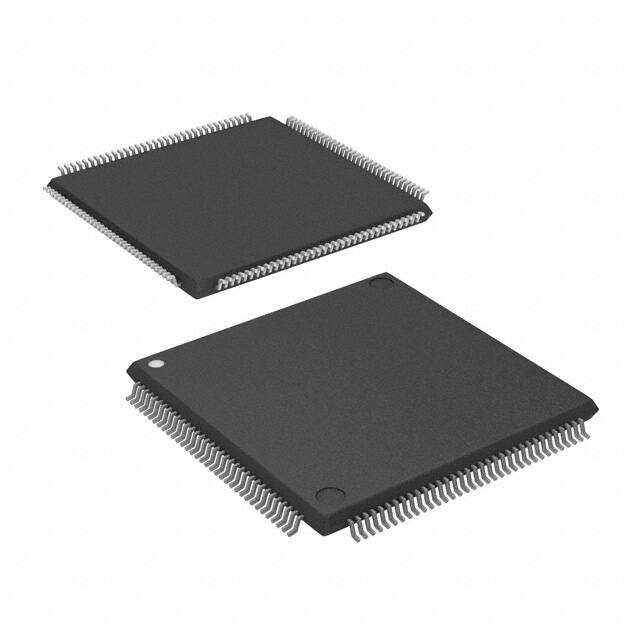


 工商网监
湘ICP备2023018690号
工商网监
湘ICP备2023018690号
