SMCJ5.0 THRU SMCJ188CA
Features
· Underwriters Laboratory recognition under UL standard for safety 497B : Isolated loop curcuit protection · Low profile package with built-in strain relief for surface mounted applications · Glass passivated junction · Low incremental surge resistance, excellent clamping capability · 1500W peak pulse power capability with a 10/1000μS waveform, repetition rate(duty cycle) : 0.01% · Very fast response time · High temperature soldering guaranteed : 250℃/10 seconds at terminals
POWER 1500Watts VOLTAGE 5.0 to 188 Volts
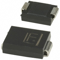
DO-214AB (SMC)
0.124(3.15) 0.108(2.75) 0.245(6.22) 0.220(5.59)
0.280(7.11) 0.260(6.60) 0.012(0.31) 0.006(0.15) 0.103(2.62) 0.079(2.00) 0.050(1.27) 0.030(0.76) 0.008(0.203) MAX. 0.320(8.13) 0.305(7.75)
Mechanical Data
· Case : JEDEC DO-214AB(SMC) molded plastic over passivated chip · Terminals : Solder plated , solderable per MIL-STD-750, method 2026 · Polarity : For uni-directional types the band denotes the cathode, which is positive with respect to the anode under normal TVS operation · Mounting Position : Any · Weight : 0.007 ounce, 0.25 gram
Dimensions in inches and (millimeters)
Devices For Bidirectional Applications
· For bi-directional devices, use suffix C or CA (e.g. SMCJ10C, SMCJ10CA). Electrical characteristics apply in both directions.
Maximum Ratings And Electrical Characteristics
(Ratings at 25℃ ambient temperature unless otherwise specified)
Symbols
Peak pulse power dissipation with a 10/1000μS waveform (Note 1,2) Peak pulse current with a waveform (Note 1) Peak forward surge current, 8.3mm single half sine-wave unidirectional only (Note 2) Typical thermal resistance, junction to ambient (Note 3) Typical thermal resistance, junction to lead Operating junction and storage temperature range PPPM IPPM IFSM
Values
Minimum 1500 See next table 200 75 15 -55 to +150
Units
Watts Amps Amps ℃/W ℃/W ℃
RθJA RθJL
TJ,TSTG
Notes:
(1) Non repetitive current pulse, per Fig.3 and derated above TA=25℃ per Fig.2 (2) Mounted on 0.31×0.31"(8.0×8.0mm) copper pads to each terminal (3) Mounted on minimum recommended pad layout
�ELECTRICAL CHARACTERISTIC
Ratings at 25℃ ambient temperature unless otherwise specified. VF=3.5V at IF=100A (uni-directional only)
Device Type S MC J 5.0(C ) S MC J 5.0(C )A(5) S MC J 6.0(C ) S MC J 6.0(C )A S MC J 6.5(C ) S MC J 6.5(C )A S MC J 7.0(C ) S MC J 7.0(C )A S MC J 7.5(C ) S MC J 7.5(C )A S MC J 8.0(C ) S MC J 8.0(C )A S MC J 8.5(C ) S MC J 8.5(C )A S MC J 9.0(C ) S MC J 9.0(C )A S MC J 10(C ) S MC J 10(C )A S MC J 11(C ) S MC J 11(C )A S MC J 12(C ) S MC J 12(C )A S MC J 13(C ) S MC J 13(C )A S MC J 14(C ) S MC J 14(C )A S MC J 15(C ) S MC J 15(C )A S MC J 16(C ) S MC J 16(C )A S MC J 17(C ) S MC J 17(C )A S MC J 18(C ) S MC J 18(C )A S MC J 20(C ) S MC J 20(C )A S MC J 22(C ) S MC J 22(C )A S MC J 24(C ) S MC J 24(C )A S MC J 26(C ) S MC J 26(C )A S MC J 28(C ) S MC J 28(C )A S MC J 30(C ) S MC J 30(C )A
Notes : (1) (2) (3) (4) (5)
Device Marking Code UNI BI G DD G DD G DE G DE G DF G DF G DG G DG G DH B DH G DK B DK G DL G DL G DM G DM G DN B DN G DP B DP G DQ B DG G DR B DR G DS B DS G DT B DT G DU B DU G DV B DV G DW B DW G DX B DX G DY G DY G DZ G DZ GE D BE D GE E BE E GE F GE F GE G GE G GE H BE H GE K BE K GE L BE L GE M BE M GE N GE N GE P GE P GE Q GE Q GE R GE R GE S BE S GE T BE T GE U BE U GE V BE V GE W BE W GE X BE X GE Y BE Y GE Z BE Z GFD BFD GFE BFE GFF BFF GFG BFG GFH BFH GFK BFK
Breakdown Voltage V(BR) at I T (1) (V) Min Max 6.40 7.82 6.40 7.07 6.67 8.15 6.67 7.37 7.22 8.82 7.22 7.98 7.78 9.51 7.78 8.60 8.33 10.2 8.33 9 .21 8.89 10.9 8.89 9.83 9.44 11.5 9.44 10.4 10.0 12.2 10.0 11.1 11.1 13.6 11.1 12.3 12.2 14.9 12.2 13.5 13.3 16.3 13.3 14.7 14.4 17.6 14.4 15.9 15.6 19.1 15.6 17.2 16.7 20.4 16.7 18.5 17.8 21.8 17.8 19.7 18.9 23.1 18.9 20.9 20.0 24.4 20.0 22.1 22.2 27.1 22.2 24.5 24.4 29.8 24.4 26.9 26.7 32.6 26.7 29.5 28.9 35.3 28.9 31.9 31.1 38.0 31.1 34.4 33.3 40.7 33.3 36.8
Test Current I T (mA) 10.0 10.0 10.0 10.0 10.0 10.0 10.0 10.0 1.0 1.0 1.0 1.0 1.0 1.0 1.0 1.0 1.0 1.0 1.0 1.0 1.0 1.0 1.0 1.0 1.0 1.0 1.0 1.0 1.0 1.0 1.0 1.0 1.0 1.0 1.0 1.0 1.0 1.0 1.0 1.0 1.0 1.0 1.0 1.0 1.0 1.0
Stand-off Voltage VWM (V) 5.0 5.0 6.0 6.0 6.5 6.5 7.0 7.0 7.5 7.5 8.0 8.0 8.5 8.5 9.0 9.0 10 10 11 11 12 12 13 13 14 14 15 15 16 16 17 17 18 18 20 20 22 22 24 24 26 26 28 28 30 30
Maximum Maximum Maximum Reverse Leakage Peak Pulse Surge Clamping at V WM Current I PPM Voltage at I PPM ID ( A) (3) μ (A) (2) VC (V) 1000 156.3 9.6 1000 163.0 9.2 1000 131.6 11.4 1000 145.6 10.3 500 122.0 12.3 500 133.9 11.2 200 112.8 13.3 200 125.0 12.0 100 104.9 14.3 100 116.3 12.9 50 100.0 15.0 50 110.3 13.6 20 94.3 15.9 20 104.2 14.4 10 88.8 16.9 10 97.4 15.4 5.0 79.8 18.8 5.0 88.2 17.0 5.0 74.6 20.1 5.0 82.4 18.2 5.0 68.2 22.0 5.0 75.4 19.9 1.0 63.0 23.8 1.0 69.8 21.5 1.0 58.1 25.8 1.0 64.7 23.2 1.0 55.8 26.9 1.0 61.5 24.4 1.0 52.1 28.8 1.0 57.7 26.0 1.0 49.2 30.5 1.0 54.3 27.6 1.0 46.6 32.2 1.0 51.4 29.2 1.0 41.9 35.8 1.0 46.3 32.4 1.0 38.1 39.4 1.0 42.3 35.5 1.0 34.9 43.0 1.0 38.6 38.9 1.0 32.2 46.6 1.0 35.6 42.1 1.0 30.0 50.0 1.0 33.0 45.4 1.0 28.0 53.5 1.0 31.0 48.4
P uls e tes t: tp 5 0ms S urge current wa ve for m per F ig. 3 and derate per F ig. 2 F or bi-directional types ha ving V WM of 10 V olts and les s , the I D limit is doubled All terms and s ymbols are cons is tent with ANS I/IE E E C 62.35 F or the bi-directional S MC G /S MC J 5.0C A, the maximum V (B R ) is 7.25V
�ELECTRICAL CHARACTERISTIC
Ratings at 25℃ ambient temperature unless otherwise specified. VF=3.5V at IF=100A (uni-directional only)
Device Type S MC J 33(C ) S MC J 33(C )A S MC J 36(C ) S MC J 36(C )A S MC J 40(C ) S MC J 40(C )A S MC J 43(C ) S MC J 43(C )A S MC J 45(C ) S MC J 45(C )A S MC J 48(C ) S MC J 48(C )A S MC J 51(C ) S MC J 51(C )A S MC J 54(C ) S MC J 54(C )A S MC J 58(C ) S MC J 58(C )A S MC J 60(C ) S MC J 60(C )A S MC J 64(C ) S MC J 64(C )A S MC J 70(C ) S MC J 70(C )A S MC J 75(C ) S MC J 75(C )A S MC J 78(C ) S MC J 78(C )A S MC J 85(C ) S MC J 85(C )A S MC J 90(C ) S MC J 90(C )A S MC J 100(C ) S MC J 100(C )A S MC J 110(C ) S MC J 110(C )A S MC J 120(C ) S MC J 120(C )A S MC J 130(C ) S MC J 130(C )A S MC J 150(C ) S MC J 150(C )A S MC J 160(C ) S MC J 160(C )A S MC J 170(C ) S MC J 170(C )A S MC J 188(C ) S MC J 188(C )A
N otes : (1) (2) (3) (4)
Device Marking Code UNI BI GFL BFL GFM BFM GFN BFN GFP BFP GFQ BFQ GFR BFR GFS BFS GFT BFT GFU GFU GFV GFV GFW GFW GFX GFX GFY GFY GFZ GFZ GGD GGD GGE GGE GGF GGF GGG GGG GGH GGH GGK GGK GGL GGL GGM GGM GGN GGN GGP GGP GGQ GGQ GGR GGR GGS GGS GGT GGT GGU GGU GGV GGV GGW GGW GGX GGX GGY GGY GGZ GGZ G HD G HD G HE G HE G HF G HF G HG G HG G HH G HH G HK G HK G HL G HL G HM G HM G HN G HN G HP G HP G HQ G HQ G HR G HR G HT G HT G HS G HS
Breakdown Voltage V(BR) at I T (1) (V) Min Max 36.7 44.9 36.7 40.6 40.0 48.9 40.0 44.2 44.4 54.3 44.4 49.1 47.8 58.4 47.8 52.8 50.0 61.1 50.0 55.3 53.3 65.1 53.3 58.9 56.7 69.3 56.7 62.7 60.0 73.3 60.0 66.3 64.4 78.7 64.4 71.2 66.7 81.5 66.7 73.7 71.1 86.9 71.1 78.6 77.8 95.1 77.8 86.0 83.3 102 83.3 92.1 86.7 106 86.7 95.8 94.4 115 94.4 104 100 122 100 111 111 136 111 123 122 149 122 135 133 163 133 147 144 176 144 159 167 204 167 185 178 218 178 197 189 231 189 2 09 209 255 209 231
Test Current I T (mA) 1.0 1.0 1.0 1.0 1.0 1.0 1.0 1.0 1.0 1.0 1.0 1.0 1.0 1.0 1.0 1.0 1.0 1.0 1.0 1.0 1.0 1.0 1.0 1.0 1.0 1.0 1.0 1.0 1.0 1.0 1.0 1.0 1.0 1.0 1.0 1.0 1.0 1.0 1.0 1.0 1.0 1.0 1.0 1.0 1.0 1.0 1.0 1.0
Stand-off Voltage VWM (V) 33 33 36 36 40 40 43 43 45 45 48 48 51 51 54 54 58 58 60 60 64 64 70 70 75 75 78 78 85 85 90 90 100 100 110 110 120 120 130 130 150 150 160 160 170 170 188 188
Maximum Maximum Maximum Reverse Leakage Peak Pulse Surge Clamping at VWM Current I PPM Voltage at I PPM ID ( A) (3) μ (A) (2) VC (V) 1.0 25.4 59.0 1.0 28.1 53.3 1.0 23.3 64.3 1.0 25.8 58.1 1.0 21.0 71.4 1.0 23.3 64.5 1.0 19.6 76.7 1.0 21.6 69.4 1.0 18.7 80.3 1.0 20.6 72.7 1.0 17.5 85.5 1.0 19.4 77.4 1.0 16.5 91.1 1.0 18.2 82.4 1.0 15.6 96.3 1.0 17.2 87.1 1.0 14.6 103 1.0 16.0 93 1.0 14.0 107 1.0 15.5 96 1.0 13.2 114 1.0 14.6 103 1.0 12.0 125 1.0 13.3 113 1.0 11.2 134 1.0 12.4 121 1.0 10.8 139 1.0 11.9 126 1.0 9.9 151 1.0 10.9 137 1.0 9.4 160 1.0 10.3 146 1.0 8.4 179 1.0 9.3 162 1.0 7.7 196 1.0 8.5 177 1.0 7.0 214 1.0 7.8 193 1.0 6.5 231 1.0 7.2 209 1.0 5.6 268 1.0 6.2 243 1.0 5.2 287 1.0 5.8 259 1.0 4.9 304 1.0 5.5 275 1.0 4.4 344 1.0 4.6 328
P uls e tes t: tp = 5 0ms S urge current wa ve for m per F ig. 3 and derate per F ig. 2 F or bi-directional types ha ving V WM of 10 V olts and les s , the I D limit is doubled All terms and s ymbols are cons is tent with ANS I/IE E E C 62.35
�RATINGS AND CHARACTERISTIC CURVES SMCJ5.0 THRU SMCJ188CA
Fig. 1ÐP eak P uls e P o wer R ating C ur ve
P eak P uls e P ower (P P P ) or C urrent (I P P ) Derating in P ercentage, %
100 100
Fig. 2Ð P uls e Derating C ur ve
P eak P uls e P ower (kW)
75
10
50
1 0.31 x 0.31" (8.0 x 8.0mm) C opper P ad A reas 0.1 0.1μs 1.0μs 1 0μs 100μs 1 .0ms 10ms
P PPM ,
25
0
0
25
50
75
100
125
150
175
200
td ,
P uls e Width (s ec.)
TA ,
A mbient Temperature ( oC )
Fig. 3Ð P uls e W a veform
150
Fig. 4Ð T ypical J unction C apacitance Uni-Directional
20,000
P eak P uls e C urrent, % I R S M
100
P eak V alue IP P M
J unction C apacitance (pF )
tr = 10μs
T J = 25 C P uls e Width (td) is defined as the point where the peak current decays to 50% of I P P M
o
10,000
Meas ured at Z ero B ias
1,000 V R , Meas ured at S tand-Off V oltage, V WM 100 Uni-Directional B i-Directional 10 T J = 25 C f = 1.0MHz V s ig = 50mV p-p 100 400
o
Half V alue IP P M 50
IP P 2
10/1000μs W aveform as defined by R .E .A. td
IP P M ,
0
0
1.0
2.0
3.0
4.0
CJ ,
1
10
t,
T ime (ms )
V WM ,
R evers e S tand-Off V oltage (V )
F ig. 5ÐT ypic al T rans ient T hermal I mpedanc e
100
Fig. 6 - Maximum Non-R epetitive Forwar d S urg e C urrent Uni-Directional Us e Onl y
200
T rans ient T hermal Impedance ( oC /W)
10
1.0
P eak F orward S urge C urrent, A mperes
100
0.1 0.001
10
0.01 0.1 1 10 100 1000
8.3ms S ingle Half S ine-W ave (J E DE C Method) T J = T J max.
1
10
100
tp ,
P uls e Duration (s ec)
Number of C ycles at 60Hz
�
很抱歉,暂时无法提供与“SMCJ110C”相匹配的价格&库存,您可以联系我们找货
免费人工找货- 国内价格
- 1+0.4875
- 10+0.45
- 30+0.4425
- 100+0.42


 工商网监
湘ICP备2023018690号
工商网监
湘ICP备2023018690号
