Click here to ask about the production status of specific part numbers.
MAX25400
Automotive Hi-Speed USB 2.0 Protector
General Description
Benefits and Features
The MAX25400 device provides high-ESD and short-circuit protection for the low-voltage internal USB data and
USB power line in automotive radio, navigation, connectivity, and USB hub applications. The device supports USB
Hi-Speed (480Mbps), USB full-speed (12Mbps), and USB
low-speed (1.5Mbps) operation. The short-circuit protection features include short-to-BUS and short-to-battery on
the protected HVD+ and HVD-, and include a fault output.
● Targeted Features for Optimized USB Performance
• Two RON 3.3Ω (typ) USB 2.0 Data Switches
• 480Mbps, 12Mbps, or 1.5Mbps USB 2.0 Operation
• 9ms Fault-Recovery Time
● Robust for the Automotive Environment
• Short-to-Battery and Short-to-BUS Protection on
Protected HVD+ and HVD- Outputs
• Tested to ISO 10605 and IEC 61000-4-2 ESD
Standards
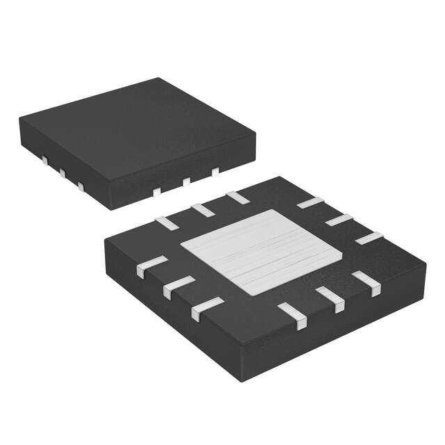
• 12-Pin (3mm x 3mm) TQFN-EP Package
• -40°C to +105°C Operating Temperature Range
• AEC-Q100 Qualified
The device features high-ESD protection to ±15kV Air Gap
and ±8kV Contact on the protected HVD+ and HVD- outputs. The device features two low on-resistance (RON)
USB 2.0 data switches.
The MAX25400 is available in a 12-pin lead-free, TQFNEP package and operate over the -40°C to 105°C temperature range.
Ordering Information appears at end of datasheet.
Applications
● Automotive USB Protection
Typical Operating Circuit
+3.3V
10uF
IN
BUS
+5V
1uF
100kΩ
FAULT
USB CONNECTOR
MAX25400
HVD+
HVD-
19-100797; Rev 1; 8/20
D+
GND
D-
LOW-VOLTAGE
USB
TRANSCEIVER
�MAX25400
Automotive Hi-Speed USB 2.0 Protector
TABLE OF CONTENTS
General Description. . . . . . . . . . . . . . . . . . . . . . . . . . . . . . . . . . . . . . . . . . . . . . . . . . . . . . . . . . . . . . . . . . . . . . . . . . . . . . 1
Applications . . . . . . . . . . . . . . . . . . . . . . . . . . . . . . . . . . . . . . . . . . . . . . . . . . . . . . . . . . . . . . . . . . . . . . . . . . . . . . . . . . . . 1
Benefits and Features . . . . . . . . . . . . . . . . . . . . . . . . . . . . . . . . . . . . . . . . . . . . . . . . . . . . . . . . . . . . . . . . . . . . . . . . . . . . 1
Typical Operating Circuit . . . . . . . . . . . . . . . . . . . . . . . . . . . . . . . . . . . . . . . . . . . . . . . . . . . . . . . . . . . . . . . . . . . . . . . . . . 1
Absolute Maximum Ratings. . . . . . . . . . . . . . . . . . . . . . . . . . . . . . . . . . . . . . . . . . . . . . . . . . . . . . . . . . . . . . . . . . . . . . . . 4
Package Information . . . . . . . . . . . . . . . . . . . . . . . . . . . . . . . . . . . . . . . . . . . . . . . . . . . . . . . . . . . . . . . . . . . . . . . . . . . . . 4
12-Pin TQFN . . . . . . . . . . . . . . . . . . . . . . . . . . . . . . . . . . . . . . . . . . . . . . . . . . . . . . . . . . . . . . . . . . . . . . . . . . . . . . . . 4
Electrical Characteristics . . . . . . . . . . . . . . . . . . . . . . . . . . . . . . . . . . . . . . . . . . . . . . . . . . . . . . . . . . . . . . . . . . . . . . . . . 4
Typical Operating Characteristics . . . . . . . . . . . . . . . . . . . . . . . . . . . . . . . . . . . . . . . . . . . . . . . . . . . . . . . . . . . . . . . . . . 8
Pin Configuration . . . . . . . . . . . . . . . . . . . . . . . . . . . . . . . . . . . . . . . . . . . . . . . . . . . . . . . . . . . . . . . . . . . . . . . . . . . . . . . . 9
MAX25400 . . . . . . . . . . . . . . . . . . . . . . . . . . . . . . . . . . . . . . . . . . . . . . . . . . . . . . . . . . . . . . . . . . . . . . . . . . . . . . . . . . 9
Pin Description . . . . . . . . . . . . . . . . . . . . . . . . . . . . . . . . . . . . . . . . . . . . . . . . . . . . . . . . . . . . . . . . . . . . . . . . . . . . . . . . . 9
Detailed Description . . . . . . . . . . . . . . . . . . . . . . . . . . . . . . . . . . . . . . . . . . . . . . . . . . . . . . . . . . . . . . . . . . . . . . . . . . . . 11
BUS Undervoltage Lockout (Power-On Reset) . . . . . . . . . . . . . . . . . . . . . . . . . . . . . . . . . . . . . . . . . . . . . . . . . . . . . 11
HVD+ and HVD- Overvoltage Protection . . . . . . . . . . . . . . . . . . . . . . . . . . . . . . . . . . . . . . . . . . . . . . . . . . . . . . . . . . 11
FAULT Output . . . . . . . . . . . . . . . . . . . . . . . . . . . . . . . . . . . . . . . . . . . . . . . . . . . . . . . . . . . . . . . . . . . . . . . . . . . . . . 11
Applications Information . . . . . . . . . . . . . . . . . . . . . . . . . . . . . . . . . . . . . . . . . . . . . . . . . . . . . . . . . . . . . . . . . . . . . . . . . 12
Power-Supply Bypass Capacitor . . . . . . . . . . . . . . . . . . . . . . . . . . . . . . . . . . . . . . . . . . . . . . . . . . . . . . . . . . . . . . . . 12
Layout of USB Data Line Traces . . . . . . . . . . . . . . . . . . . . . . . . . . . . . . . . . . . . . . . . . . . . . . . . . . . . . . . . . . . . . . . . 12
±25kV ESD Protection . . . . . . . . . . . . . . . . . . . . . . . . . . . . . . . . . . . . . . . . . . . . . . . . . . . . . . . . . . . . . . . . . . . . . . . . 12
ESD Test Conditions . . . . . . . . . . . . . . . . . . . . . . . . . . . . . . . . . . . . . . . . . . . . . . . . . . . . . . . . . . . . . . . . . . . . . . . . . 12
Human Body Model . . . . . . . . . . . . . . . . . . . . . . . . . . . . . . . . . . . . . . . . . . . . . . . . . . . . . . . . . . . . . . . . . . . . . . . . . . 12
IEC 61000-4-2 . . . . . . . . . . . . . . . . . . . . . . . . . . . . . . . . . . . . . . . . . . . . . . . . . . . . . . . . . . . . . . . . . . . . . . . . . . . . . . 12
Human Body Test Model . . . . . . . . . . . . . . . . . . . . . . . . . . . . . . . . . . . . . . . . . . . . . . . . . . . . . . . . . . . . . . . . . . . . . . 13
Human Body Current Waveform . . . . . . . . . . . . . . . . . . . . . . . . . . . . . . . . . . . . . . . . . . . . . . . . . . . . . . . . . . . . . . . . 14
IEC 61000-4-2 ESD Test Model . . . . . . . . . . . . . . . . . . . . . . . . . . . . . . . . . . . . . . . . . . . . . . . . . . . . . . . . . . . . . . . . . 15
IEC 61000-4-2 ESD Generator Current Waveform . . . . . . . . . . . . . . . . . . . . . . . . . . . . . . . . . . . . . . . . . . . . . . . . . . 16
Functional Diagram . . . . . . . . . . . . . . . . . . . . . . . . . . . . . . . . . . . . . . . . . . . . . . . . . . . . . . . . . . . . . . . . . . . . . . . . . . 17
Ordering Information . . . . . . . . . . . . . . . . . . . . . . . . . . . . . . . . . . . . . . . . . . . . . . . . . . . . . . . . . . . . . . . . . . . . . . . . . . . . 17
Revision History . . . . . . . . . . . . . . . . . . . . . . . . . . . . . . . . . . . . . . . . . . . . . . . . . . . . . . . . . . . . . . . . . . . . . . . . . . . . . . . 18
www.maximintegrated.com
Maxim Integrated | 2
�MAX25400
Automotive Hi-Speed USB 2.0 Protector
LIST OF FIGURES
Figure 1. Timing Diagram for Undervoltage Lockout on BUS . . . . . . . . . . . . . . . . . . . . . . . . . . . . . . . . . . . . . . . . . . . . . . 6
Figure 2. Timing Diagram for Overvoltage Protection on HVD+, HVD-. . . . . . . . . . . . . . . . . . . . . . . . . . . . . . . . . . . . . . . 6
Figure 3. On-Channel -3dB Bandwidth and Crosstalk . . . . . . . . . . . . . . . . . . . . . . . . . . . . . . . . . . . . . . . . . . . . . . . . . . . 6
Figure 4. On-Capacitance . . . . . . . . . . . . . . . . . . . . . . . . . . . . . . . . . . . . . . . . . . . . . . . . . . . . . . . . . . . . . . . . . . . . . . . . . 7
Figure 5. Propagation Delay and Output Skew . . . . . . . . . . . . . . . . . . . . . . . . . . . . . . . . . . . . . . . . . . . . . . . . . . . . . . . . . 7
Figure 6. Human Body ESD Test Model . . . . . . . . . . . . . . . . . . . . . . . . . . . . . . . . . . . . . . . . . . . . . . . . . . . . . . . . . . . . . 13
Figure 7. Human Body Current Waveform . . . . . . . . . . . . . . . . . . . . . . . . . . . . . . . . . . . . . . . . . . . . . . . . . . . . . . . . . . . 14
Figure 8. IEC 61000-4-2 ESD Test Model. . . . . . . . . . . . . . . . . . . . . . . . . . . . . . . . . . . . . . . . . . . . . . . . . . . . . . . . . . . . 15
Figure 9. IEC 61000-4-2 ESD Generator Current Waveform . . . . . . . . . . . . . . . . . . . . . . . . . . . . . . . . . . . . . . . . . . . . . 16
Figure 10. Functional Diagram . . . . . . . . . . . . . . . . . . . . . . . . . . . . . . . . . . . . . . . . . . . . . . . . . . . . . . . . . . . . . . . . . . . . 17
www.maximintegrated.com
Maxim Integrated | 3
�MAX25400
Automotive Hi-Speed USB 2.0 Protector
Absolute Maximum Ratings
BUS, IN..................................................................... -0.3V to +6V
FAULT, D+, D-.......................................................... -0.3V to +6V
D+, D- to IN ......................................................................... +0.3V
HVD+, HVD- ........................................................... -0.3V to +18V
Continuous Power Dissipation 12-Pin TQFN (Four Layer Board
derate 21.3mW/°C above +70°C) (TA = +70°C) ............ 1704mW
Operating Ambient Temperature Range.............-40°C to +105°C
Maximum Junction Temperature ...................................... +150°C
Storage Temperature Range ..............................-60°C to +150°C
Lead Temperature (soldering) (10s) ................................. +300°C
Soldering Temperature (reflow) ........................................ +260°C
Stresses beyond those listed under “Absolute Maximum Ratings” may cause permanent damage to the device. These are stress ratings only, and functional operation of the
device at these or any other conditions beyond those indicated in the operational sections of the specifications is not implied. Exposure to absolute maximum rating conditions for
extended periods may affect device reliability.
Package Information
12-Pin TQFN
Package Code
T1233+5C
Outline Number
21-0136
Land Pattern Number
90-0019
THERMAL RESISTANCE, FOUR-LAYER BOARD
Junction-to-Ambient (θJA)
46.9°C/W
Junction-to-Case Thermal Resistance (θJC)
5.27°C/W
For the latest package outline information and land patterns (footprints), go to www.maximintegrated.com/packages.
Note that a “+”, “#”, or “-” in the package code indicates RoHS status only. Package drawings may show a different
suffix character, but the drawing pertains to the package regardless of RoHS status.
Package thermal resistances were obtained using the method described in JEDEC specification JESD51-7, using a
four-layer board. For detailed information on package thermal considerations, refer to www.maximintegrated.com/
thermal-tutorial.
Electrical Characteristics
(VBUS = 5.0V VIN = +3.3V, TJ = TA = -40°C to +105°C. RL = ∞, unless otherwise noted. Typical values are at TA = +25°C, unless
otherwise noted. (Note 1))
PARAMETER
SYMBOL
CONDITIONS
MIN
TYP
MAX
UNITS
POWER SUPPLY
Power Supply Range
(BUS)
VBUS
4.75
5.5
V
Power Supply Range
(IN)
VIN
3.0
3.6
V
BUS Input Current
IBUS
No load, no fault
VIN Input Current
IIN
No load, no fault
BUS Undervoltage
Lockout
VUVLO
VBUS falling (Figure 1)
VOV_D
HVD+, HVD- rises from VIN to > VIN+1V
(Figure 2)
125
3.85
4.2
μA
12
μA
4.55
V
3.6
V
3.9
V
USB DATA SWITCH
Analog Signal Range
Protection-Trip
Threshold
www.maximintegrated.com
0
Maxim Integrated | 4
�MAX25400
Automotive Hi-Speed USB 2.0 Protector
Electrical Characteristics (continued)
(VBUS = 5.0V VIN = +3.3V, TJ = TA = -40°C to +105°C. RL = ∞, unless otherwise noted. Typical values are at TA = +25°C, unless
otherwise noted. (Note 1))
PARAMETER
SYMBOL
Protection-Recovery
Time
tFPR_D
Protection-Response
Time
tFP_D
On-Resistance
RON
On-Resistance Match
Between Channels
ΔRON
CONDITIONS
MIN
TYP
MAX
UNITS
6
9
11
ms
HVD+, HVD- rises from VIN to > VIN+1V
(Figure 2)
0.5
1
μs
VBUS = 5V, IL = 40mA, 0 ≤ VD ≤ 3.6V
3.3
HVD+, HVD- falling to below VOV_D
(Figure 2)
Ω
VBUS = 5V, IL = 40mA, VD = 1.5V, 3.0V
0.25
Ω
IL = 40mA, VD = 0V or 0.4V
0.25
Ω
On-Resistance Flatness
RFLAT(ON)
HVD+, HVD- OffLeakage Current
VHVD+ , VHVD- = 18V, VD+ , VD- = 0V
20
IHVD_OFF
VHVD+ , VHVD- = 18V, VD+, VD = 0V, VIN
= 0V, VBUS = 0V
20
HVD+, HVD- OnLeakage Current
IHVD_ON
VHVD+, VHVD- = VIN
5
On Channel -3dB
Bandwidth
BW
RL = 50Ω, source Impedance = 50Ω
(Figure 5)
VOL
ISINK = 500μA
864
µA
µA
MHz
FAULT OUTPUT
FAULT Output Low
Voltage
FAULT Output HighLeakage Current
FAULT Recovery Time
tFPR
VFAULT = VIN (Figure 3)
6
9
0.5
V
1
μA
11
ms
ESD PROTECTION D+, D-, BUS, FAULTB, VIN
ESD Protection Level
VESD
Human Body Model
±2
ISO 10605 Air Gap (330pF, 2kΩ)
±25
kV
ESD PROTECTION HVD+, HVD-
ESD Protection Level
VESD
ISO 10605 Contact (330pF, 2kΩ)
±8
IEC 61000-4-2 Air Gap (150pF, 330Ω)
± 25
IEC 61000-4-2 Contact (150pF, 330Ω)
±8
kV
Thermal Protection
Thermal Shutdown
165
°C
Thermal Shutdown
Hysteresis
15
°C
Note 1: Specifications with minimum and maximum limits are 100% production tested at TA = +25°C and are guaranteed over the
operating temperature range by design and characterization. Actual typical values may vary and are not guaranteed.
Note 2: Guaranteed by design. Limits are not production tested.
Note 3: Tested in the Typical Application Circuit, as shown on the evaluation kit.
www.maximintegrated.com
Maxim Integrated | 5
�MAX25400
Automotive Hi-Speed USB 2.0 Protector
VUVLO
VBUS
GND
ON
OFF
ON
DEVICE
tFPR_BUS
FAULT
GND
Figure 1. Timing Diagram for Undervoltage Lockout on BUS
VOV_D
GND
ON
OFF
ON
tFP_D
DEVICE
tFP_BUS
tFPR_D
tFPR_BUS
FAULT
GND
Figure 2. Timing Diagram for Overvoltage Protection on HVD+, HVD-
NETWORK
ANALYZER
D+
(D-)
50
V IN
ON-LOSS = 20log
VIN
VOUT
CROSSTALK = 20log
MAX25400
HVD+
VOUT
50
V OUT
MEAS
VIN
ON-LOSS1 = 20log
HVD+
ON-LOSS2 = 20log
HVD-
REF
(HVD-)
D+
D-
50
50
CROSSTALK1 = 20log
HVD+
CROSSTALK2 = 20log
HVD-
D-
GND
D+
ON-LOSS IS MEASURED BETWEEN D+ AND HVD+, OR D- AND HVD-.
CROSSTALK IS MEASURED FROM ONE CHANNEL TO THE OTHER CHANNEL.
SIGNAL DIRECTION THROUGH SWITCH IS REVERSED; WORST VALUES ARE RECORDED.
Figure 3. On-Channel -3dB Bandwidth and Crosstalk
www.maximintegrated.com
Maxim Integrated | 6
�MAX25400
Automotive Hi-Speed USB 2.0 Protector
MAX25400
D_ OR
HVD_
CAPACITANCE
METER
GND
Figure 4. On-Capacitance
MAX25400
RS
INPUT+
D+
HVD+
OUT+
RISE-TIME PROPAGATION DELAY = tPLHX OR tPHLY
FALL-TIME PROPAGATION DELAY = tPLHX OR tPHLY
tSKB = |tPHLX - tPHLY| OR |tPLHX - tPHLY|
tSKS = |tPLHX - tPHLX| OR |tPLHY - tPHLY|
RL
RS
INPUT-
D-
HVD-
OUTRL
EN
V TO V
IL
IH
t INFALL
t INRISE
V+
90%
V INPUT+
50%
90%
50%
10%
0V
10%
V+
V INPUT-
50%
50%
0V
t OUTRISE
t PLHX
t OUTFALL
t PHLX
V+
90%
V OUT+
90%
50%
50%
10%
0V
10%
V+
50%
V OUT -
50%
0V
t PHLY
t PLHY
Figure 5. Propagation Delay and Output Skew
www.maximintegrated.com
Maxim Integrated | 7
�MAX25400
Automotive Hi-Speed USB 2.0 Protector
Typical Operating Characteristics
(TA = 25ºC , unless otherwise noted)
toc04
toc02
toc03
toc05
toc06
toc07
www.maximintegrated.com
Maxim Integrated | 8
�MAX25400
Automotive Hi-Speed USB 2.0 Protector
Typical Operating Characteristics (continued)
(TA = 25ºC , unless otherwise noted)
CROSSTALK
0
SINGLE - ENDED BANDWIDTH
toc12
0
toc11
--0.4
-20
-30
-40
864 MHz
-3
|S21| (dB)
DIFFERENTIAL SIGNAL (V)
-10
CROSSTALK (dB)
USB 2.0 HIGH -SPEED EYE DIAGRAM
(NO TUNING COMPONENTS)
toc10
0
-6
-9
-50
--0.4
-60
10
100
FREQUENCY (MHz)
1000
-12
0
1
10
2
100
1000
FREQUENCY (MHz)
TIME (ns)
Pin Configuration
MAX25400
GND
11
GND
12
D-
GND
8
7
MAX25400
+
HVD+
1
2
3
FAULT
10
9
HVD-
IN
D+
TOP VIEW
TQFN
3mm x 3mm
6
BUS
5
N.C.
4
GND
Pin Description
PIN
NAME
1
HVD+
High-Voltage-Protected USB Differential Data D+ Output. Connect HVD+ directly to USB
connector D+.
2
HVD-
High-Voltage-Protected USB Differential Data D- Output. Connect HVD- directly to USB connector
D-.
3
FAULT
5
N.C.
No Connection. Internally connected to IC ground.
6
BUS
Main IC Supply. Connect BUS to USB +5V supply. Connect a 1μF, low-ESR ceramic capacitor
from BUS to GND.
www.maximintegrated.com
FUNCTION
Open-Drain Fault Condition Indicator Output.
Maxim Integrated | 9
�MAX25400
Automotive Hi-Speed USB 2.0 Protector
Pin Description (continued)
PIN
NAME
FUNCTION
8
D-
USB Differential Data D- Input. Connect D- to low-voltage USB transceiver D-.
9
D+
USB Differential Data D+ Input. Connect D+ to low-voltage USB transceiver D+.
10
IN
Logic Power-Supply Input. The supply voltage range is from +3.0V to +3.6V. Bypass IN to GND
with a 10μF ceramic capacitor.
4, 7, 11, 12
GND
www.maximintegrated.com
Ground
Maxim Integrated | 10
�MAX25400
Automotive Hi-Speed USB 2.0 Protector
Detailed Description
The MAX25400 device provides high-ESD and short-circuit protection for the USB data in automotive radio, navigation,
connectivity, and USB hub applications. The device supports USB Hi-Speed (480Mbps), USB full-speed (12Mbps), and
USB low-speed (1.5Mbps) operation.
The short-circuit protection features include short-to-BUS and short-to-battery on the protected HVD+ and HVD-.
The device features high-ESD protection to ±25kV Air Gap Discharge and ±8kV Contact Discharge on all
protected HVD+ and HVD- outputs.
The device features two low on-resistance (RON), USB 2.0 switches.
BUS Undervoltage Lockout (Power-On Reset)
The device has a 4.2V (typ) undervoltage-lockout threshold (VUVLO). When VBUS is less than VUVLO, FAULT is enabled
and all the device switches are high impedance.
HVD+ and HVD- Overvoltage Protection
The device has a 3.9V (max) overvoltage threshold (VOV_D). When HVD+ or HVD- is greater than VOV_D, FAULT
asserts low and all the device switches are high impedance. Note that HVD+ and HVD- do not have short-to-ground
protection. Forward current is limited by the upstream transceiver.
FAULT Output
FAULT goes low when a fault is detected on HVD+, HVD-. FAULT indicates if any of the following conditions exist:
overvoltage on HVD-, HVD+; UVLO on VBUS; or overtemperature. Connect a 100kΩ pullup resistor from FAULT to IN.
www.maximintegrated.com
Maxim Integrated | 11
�MAX25400
Automotive Hi-Speed USB 2.0 Protector
Applications Information
Power-Supply Bypass Capacitor
Connect a 1μF low-ESR ceramic capacitor from BUS to GND. Connect a 10μF ceramic capacitor from IN to GND. Place
these components on the same plane as the IC, close to the IN and GND pins.
Layout of USB Data Line Traces
USB Hi-Speed requires careful PCB layout with 90Ω controlled-impedance matched traces of equal lengths. Use LC
tuning components on the data lines, as shown in the Typical Operating Circuit. The values of these components are
layout and captive-cable dependent. Contact Maxim technical support for more detailed information.
±25kV ESD Protection
As with all Maxim devices, ESD-protection structures are incorporated on all pins to protect against electrostatic
discharges encountered during handling and assembly. The device has extra protection against static electricity. Maxim’s
engineers have developed state-of-the-art structures to protect against ESD of ±25kV at the HVD+, HVD- ports without
damage. The ESD structures withstand high ESD in all states: normal operation, shutdown, and powered down. After an
ESD event, the device keeps working without latchup, whereas other solutions can latch and must be powered down to
remove latchup. ESD protection can be tested in various ways; this product is characterized for protection to the following
limits:
● ±2kV using the Human Body Model
● ±25kV using IEC 61000-4-2’s Air-Gap Discharge method
● ±8kV using the Contact Discharge method specified in IEC 61000-4-2
ESD Test Conditions
ESD performance depends on a variety of conditions. Contact Maxim for a reliability report that documents test setup,
test methodology, and test results.
Human Body Model
Figure 6 shows the Human Body Model, and Figure 7 shows the current waveform it generates when discharged into
a low impedance. This model consists of a 100pF capacitor charged to the ESD voltage of interest, which is then
discharged into the device through a 1.5kΩ resistor.
IEC 61000-4-2
The IEC 61000-4-2 standard covers ESD testing and performance of finished equipment. The MAX25400 helps users
design equipment that meets Level 4 of IEC 61000-4-2. The main difference between tests done using the Human
Body Model and IEC 61000-4-2 is higher peak current in IEC 61000-4-2. Because series resistance is lower in the IEC
61000-4-2 ESD test model (Figure 8), the ESD withstand voltage measured to this standard is generally lower than that
measured using the Human Body Model. Figure 9 shows the current waveform for the ±8kV, IEC 61000-4-2 Level 4, ESD
Contact Discharge test. The Air-Gap Discharge test involves approaching the device with a charged probe. The Contact
Discharge method connects the probe to the device before the probe is energized.
www.maximintegrated.com
Maxim Integrated | 12
�MAX25400
Automotive Hi-Speed USB 2.0 Protector
Human Body Test Model
RC
1MΩ
RD
1.5kΩ
CHARGE-CURRENT-LIMIT
RESISTOR
DISCHARGE
RESISTANCE
HIGH-VOLTAGE
DC
SOURCE
CS
100pF
STORAGE
CAPACITOR
DEVICE
UNDER
TEST
Figure 6. Human Body ESD Test Model
www.maximintegrated.com
Maxim Integrated | 13
�MAX25400
Automotive Hi-Speed USB 2.0 Protector
Human Body Current Waveform
IPEAK
(AMPS)
100%
IR
90%
36.8%
10%
t
0
0
tRL
tDL
Figure 7. Human Body Current Waveform
www.maximintegrated.com
Maxim Integrated | 14
�MAX25400
Automotive Hi-Speed USB 2.0 Protector
IEC 61000-4-2 ESD Test Model
RC
50Ω to 100Ω
RD
330Ω
CHARGE-CURRENT-LIMIT
RESISTOR
DISCHARGE
RESISTANCE
HIGH-VOLTAGE
DC
SOURCE
CS
150pF
STORAGE
CAPACITOR
DEVICE
UNDER
TEST
Figure 8. IEC 61000-4-2 ESD Test Model
www.maximintegrated.com
Maxim Integrated | 15
�MAX25400
Automotive Hi-Speed USB 2.0 Protector
IEC 61000-4-2 ESD Generator Current Waveform
100%
IPEAK (AMPS)
90%
10%
t
tR = 0.7ns TO 1ns
30ns
60ns
Figure 9. IEC 61000-4-2 ESD Generator Current Waveform
www.maximintegrated.com
Maxim Integrated | 16
�MAX25400
Automotive Hi-Speed USB 2.0 Protector
Functional Diagram
BUS
LV ESD
CLAMP
UNDERVOLTAGE
LOCKOUT
OVP (SHORT-TOBATTERY AND/OR
SHORT-TO-VBUS
FAULT
CONTROL
IN
THERMAL
SHUTDOWN
LV ESD
CLAMP
HVD+
D+
IEC
SCR
CLAMP
HVD-
DIEC
SCR
CLAMP
MAX25400
GND
Figure 10. Functional Diagram
Ordering Information
PART NUMBER
MAX25400GTC/V+
TEMPERATURE RANGE
PIN-PACKAGE
-40°C TO +105°C
12 TQFN-EP*
/V denotes an automotive qualified part.
+Denotes a lead(Pb)-free/RoHS-compliant package.
*EP = Exposed pad.
www.maximintegrated.com
Maxim Integrated | 17
�MAX25400
Automotive Hi-Speed USB 2.0 Protector
Revision History
REVISION
NUMBER
REVISION
DATE
0
4/20
Initial release
8/20
Updated Typical Operating Circuit, Package Information, Electrical Characteristics, Pin
Description, Detailed Description, and Applications Information
1
PAGES
CHANGED
DESCRIPTION
—
1, 4–7, 9,
10–17
For pricing, delivery, and ordering information, please visit Maxim Integrated’s online storefront at https://www.maximintegrated.com/en/storefront/storefront.html.
Maxim Integrated cannot assume responsibility for use of any circuitry other than circuitry entirely embodied in a Maxim Integrated product. No circuit patent
licenses are implied. Maxim Integrated reserves the right to change the circuitry and specifications without notice at any time. The parametric values (min and max
limits) shown in the Electrical Characteristics table are guaranteed. Other parametric values quoted in this data sheet are provided for guidance.
Maxim Integrated and the Maxim Integrated logo are trademarks of Maxim Integrated Products, Inc.
© 2020 Maxim Integrated Products, Inc.
�


 工商网监
湘ICP备2023018690号
工商网监
湘ICP备2023018690号
