S1C31W74
(rev1.1)
32-bit Single Chip Microcontroller
●
●
●
●
■ DESCRIPTIONS
ARM® 32-bit RISC CPU core Cortex®-M0+
Embedded 72SEG × 32COM LCD driver
Embedded 512K-byte Flash memory and 128K-byte RAM
Various interfaces such as UART, QSPI, I2C, and USB that support
DMA transfer
The S1C31W74 is a 32-bit MCU with an ARM® Cortex®-M0+ processor included that features low-power operation. It
incorporates an LCD driver capable of driving up to a 2,304-dot LCD panel, a large-capacity Flash memory, and a lot of
serial interface circuits. The S1C31W74 is suitable for various kinds of battery-driven controller applications.
■ FEATURES
Model
CPU
CPU core
Other
Embedded Flash memory
Capacity
Erase/program count
Other
Embedded RAMs
General-purpose RAM
Display RAM
Instruction cache
DMA controller (DMAC)
Number of channels
Data transfer path
Transfer mode
DMA trigger source
Clock generator (CLG)
System clock source
System clock frequency (operating frequency)
IOSC oscillator circuit (boot clock source)
OSC1 oscillator circuit
OSC3 oscillator circuit
EXOSC clock input
Other
I/O port (PPORT)
Number of general-purpose I/O ports
Number of input interrupt ports
Number of ports that support universal port
multiplexer (UPMUX)
Timers
Watchdog timer (WDT2)
Real-time clock (RTCA)
16-bit timer (T16)
16-bit PWM timer (T16B)
S1C31W74
ARM® 32-bit RISC CPU core Cortex®-M0+
Serial-wire debug ports (SW-DP) and a micro trace buffer (MTB) included
512K bytes (for both instructions and data)
1,000 times (min.) * When being programmed by the dedicated flash loader
On-board programming function
Flash programming voltage can be generated internally.
128K bytes (shared with MTB)
704 bytes
512 bytes
4 channels
Memory to memory, memory to peripheral, and peripheral to memory
Basic, ping-pong, scatter-gather
UART2, SPIA, QSPI, I2C, USB, T16B, SNDA, and software
4 sources (IOSC/OSC1/OSC3/EXOSC)
VD1 voltage mode = mode0: 21 MHz (max.)
VD1 voltage mode = mode1: 2.1 MHz (max.)
VD1 voltage mode = mode0: 20/16/12/8/2/1 MHz (typ.) software selectable
VD1 voltage mode = mode1: 2/1 MHz (typ.) software selectable
10 µs (max.) starting time (time from cancelation of SLEEP state to vector table read by
the CPU)
32.768 kHz (typ.) crystal oscillator
Oscillation stop detection circuit included
20.5 MHz (max.) crystal/ceramic oscillator
21 MHz (max.) square or sine wave input
Configurable system clock division ratio
Configurable system clock used at wake up from SLEEP state
Operating clock frequency for the CPU and all peripheral circuits is selectable.
71 bits (max.)
Pins are shared with the peripheral I/O.
67 bits (max.)
24 bits
A peripheral circuit I/O function selected via software can be assigned to each port.
Generates NMI or watchdog timer reset.
Programmable NMI/reset generation cycle
128–1 Hz counter, second/minute/hour/day/day of the week/month/year counters
Theoretical regulation function for 1-second correction
Alarm and stopwatch functions
4 channels
Generates the SPIA and QSPI master clocks.
2 channels
Event counter/capture function
PWM waveform generation function
Number of PWM output or capture input ports: 2 ports/channel
®
�S1C31W74
Supply voltage detector (SVD2)
Number of channels
Detection level
Other
Serial interfaces
UART (UART2)
Synchronous serial interface (SPIA)
Quad synchronous serial interface (QSPI)
I2C (I2C)
USB 2.0 FS device controller (USB)
Number of transceiver/receiver channels
Transfer rate
Clock source
Number of endpoints
Power supply
Sound generator (SNDA)
Buzzer output function
Melody generation function
IR remote controller (REMC2)
Number of transmitter channels
Other
LCD driver (LCD32B)
LCD output
LCD contrast
Other
R/F converter (RFC)
Conversion method
Number of conversion channels
Supported sensors
Reset
#RESET pin
Power-on reset
Brownout reset
Key entry reset
Watchdog timer reset
Supply voltage detector reset
Interrupt
Non-maskable interrupt
Programmable interrupt
Power supply voltage
VDD operating voltage
VDD operating voltage for Flash programming
VDD operating voltage when LCD driver is used
Operating temperature
Operating temperature range
Current consumption (Typ. value)
SLEEP mode *1
2
2 channels
32 levels (1.7 to 4.3 V)
Intermittent operation mode
Generates an interrupt or reset (Ch.0) according to the detection level evaluation.
2 channels
Baud-rate generator included, IrDA1.0 supported
Open drain output, signal polarity, and baud rate division ratio are configurable.
1 channel
2 to 16-bit variable data length
The 16-bit timer (T16) can be used for the baud-rate generator in master mode.
1 channel
Supports single, dual, and quad transfer modes.
Low CPU overhead memory mapped access mode that can directly read data from the
external flash memory with XIP (eXecute-In-Place) mode.
2 channels
Baud-rate generator included
1 channel
FS (12 Mbps)
48 MHz crystal oscillator or OSC3 (12 MHz) + PLL selectable
4 endpoints (3 general-purpose endpoints and endpoint 0)
Voltage regulators for USB included
512 Hz to 16 kHz output frequencies
One-shot output function
Pitch:
128 Hz to 16 kHz ≈ C3 to C6
Duration: 7 notes/rests (Half note/rest to thirty-second note/rest)
Tempo: 16 tempos (30 to 480)
Tie/slur may be specified.
1 channel
EL lamp drive waveform can be generated (by the hardware) for an application example.
88SEG × 1–16COM (max.), 80SEG × 17–24COM (max.), 72SEG × 25–32COM (max.)
16 levels
1/5 or 1/4 bias power supply included, external voltage can be applied.
CR oscillation type with 24-bit counters
1 channel (Up to two sensors can be connected.)
DC-bias resistive sensors, AC-bias resistive sensors
Reset when the reset pin is set to low.
Reset at power on.
Reset when the power supply voltage drops (when VDD ≤ 1.45 V (typ.) is detected).
Reset when the P00 to P01/P02/P03 keys are pressed simultaneously (can be enabled/
disabled using a register).
Reset when the watchdog timer overflows (can be enabled/disabled using a register).
Reset when the supply voltage detector detects the set voltage level (can be enabled/disabled using a register).
6 systems (Reset, NMI, HardFault, SVCall, PendSV, SysTic)
External interrupt: 1 system
Internal interrupt: 23 systems
1.8 to 3.6 V
2.7 to 3.6 V (when the internal voltage booster is used)
2.5 to 3.6 V
-40 to 85 °C
0.4 µA
IOSC = OFF, OSC1 = OFF, OSC3 = OFF
0.9 µA
IOSC = OFF, OSC1 = ON, OSC3 = OFF, RTC = ON
Seiko Epson Corporation
�S1C31W74
Current consumption (Typ. value)
HALT mode *2
RUN mode
Shipping form
1
2
1.7 µA
OSC1 = 32 kHz
7.7 µA
OSC1 = 32 kHz, LCD = ON (no panel load)
250 µA/MHz
VD1 voltage mode = mode0, CPU = IOSC
150 µA/MHz
VD1 voltage mode = mode1, CPU = IOSC
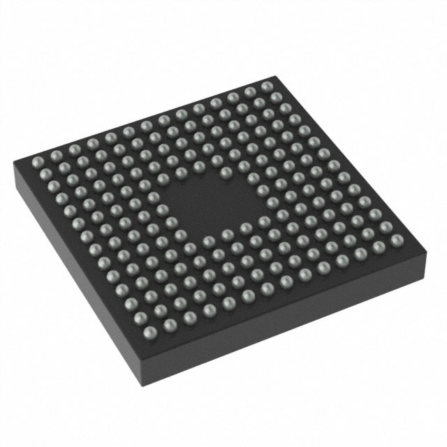
VFBGA8HX-181 (size: 8 × 8 mm, ball pitch: 0.5 mm)
Die form (pad pitch: 80 µm (min.))
*1 SLEEP mode refers to deep sleep mode in the Cortex®-M0+ processor.
*2 HALT mode refers to sleep mode in the Cortex®-M0+ processor.
■ BLOCK DIAGRAM
MTB
Cache RAM
512 bytes
RAM
128K bytes
Flash memory
512K bytes
Display RAM
704 bytes
CPU core, interrpt controller, and debuger
(Cortex®-M0+)
VPP
DMA controller
System clock
16-bit peripheral bus
DMA request signal
32-bit AHB bus
SWCLK
SWD
Cache controller
USB 2.0 FS
device controller
(USB)
USB_DP
USB_DM
VBUS
USB_XI
USB_XO
USB33VOUT
USB18VOUT
Quad
synchronous
serial interface
(QSPI)
1 Ch.
QSDIO00–03
QSPICLK0
#QSPISS0
Synchronous
serial interface
(SPIA)
1 Ch.
SDI0
SDO0
SPICLK0
#SPISS0
I2C
(I2C)
2 Ch.
SDA0–1
SCL0–1
IR remote
controller
(REMC2)
1 Ch.
REMO
CLPLS
Interrupt signal
Clock generator
(CLG)
FOUT
IOSC
oscillator
OSC1
OSC2
OSC1
oscillator
OSC3
OSC4
OSC3
oscillator
EXOSC
EXOSC
input circuit
System reset controller
(SRC)
#RESET
VDD
VSS
VD1
I/O port
(PPORT)
P00–07
P10–17
P20–27
P30–37
P40–47
P50–57
P60–67
P70–77
P80–81
P90
PD0–D3
Watchdog timer
(WDT2)
Real-time clock
(RTCA)
RTC1S
Brownout reset
(BOR)
Supply voltage
detector
(SVD2)
2 Ch.
EXSVD0
VBUS_MON
(EXSVD1)
Power generator
(PWGA)
16-bit timer
(T16)
4 Ch.
Power-on reset
(POR)
16-bit PWM timer
(T16B)
2 Ch.
TOUT00–01
TOUT10–11
CAP00–01
CAP10–11
EXCL00–01
EXCL10–11
UART
(UART2)
2 Ch.
USIN0–1
USOUT0–1
Seiko Epson Corporation
Sound generator
(SNDA)
BZOUT
#BZOUT
LCD driver
(LCD32B)
COM0–31
SEG0–87
LFRO
VC1–5
CP1–5
R/F converter
(RFC)
1 Ch.
RFIN0
REF0
SENA0
SENB0
RFCLKO0
3
�S1C31W74
■ PIN CONFIGURATION DIAGRAMS
VFBGA8HX-181
Top View
A1 Corner
A
B
C
D
E
F
G
H
J
K
L
M
N
P
Bottom View
A
B
C
D
E
F
G
H
J
K
L
M
N
P
Index
1 2 3 4 5 6 7 8 9 10 11 12 13 14
N.C.
1
CP5
2
CP4
3
A1 Corner
14 13 12 11 10 9 8 7 6 5 4 3 2 1
4
SEG14
5
SEG19
6
SEG23
7
SEG27
8
SEG31
9
SEG35
10
SEG39
11
SEG44
12
SEG45
13
SEG47
14
N.C.
A
VC3
VC1
CP3
SEG15
SEG18
SEG22
SEG26
SEG30
SEG34
SEG38
SEG43
SEG46
SEG48
SEG50
SEG13
VC4
VC2
CP1
SEG17
SEG21
SEG25
SEG29
SEG33
SEG37
SEG42
SEG49
SEG51
SEG52
SEG10
P70
SEG9
SEG12
CP2
SEG16
SEG20
SEG24
SEG28
SEG32
SEG36
SEG53
SEG54
SEG55
P67
SEG56
P75
SEG4
P73
SEG6
P71
SEG8
SEG11
VC5
VDD
VDD
VSS
SEG40
SEG41
P66
SEG57
P65
SEG58
P64
SEG59
P63
SEG60
P81
SEG0
P76
SEG3
P77
SEG2
P72
SEG7
VSS
VSS
P56
SEG65
P62
SEG61
P61
SEG62
P60
SEG63
P57
SEG64
COM12
COM15
COM14
P80
SEG1
P74
SEG5
P51
SEG70
P55
SEG66
P54
SEG67
P53
SEG68
P52
SEG69
COM8
COM11
COM10
COM13
VSS
VDD
P50
SEG71
P47
COM31
SEG72
P46
COM30
SEG73
P45
COM29
SEG74
COM4
COM7
COM6
COM9
VSS
P40
COM24
SEG79
P44
COM28
SEG75
P43
COM27
SEG76
P42
COM26
SEG77
P41
COM25
SEG78
COM0
COM3
COM2
COM5
VDD
VDD
P17
RTC1S
UPMUX
P22
VSS
QSDIO01
USB_XI
USB18
VOUT
COM1
VSS
VSS
P12
EXCL00
UPMUX
P16
CLPLS
UPMUX
P21
P23
QSDIO00 QSDIO02
P37
UPMUX
COM23
SEG80
VDD
P33
UPMUX
COM19
SEG84
P27
EXSVD0
P34
UPMUX
COM20
SEG83
P30
LFRO
P35
UPMUX
COM21
SEG82
P31
P00
SDI0
UPMUX
VSS
P11
P15
#BZOUT REMO
UPMUX UPMUX
SWCLK
PD0
TEST
P36
UPMUX
COM22
SEG81
P32
UPMUX
COM18
SEG85
VPP
P01
SDO0
UPMUX
P03
P05
#SPISS0 SENA0
UPMUX UPMUX
B
C
D
E
F
G
Top View
H
J
K
L
USB_XO VSS
VBUS
VSS
USB33
VOUT
VBUS
M
N
N.C.
P
4
VSS
P90
EXSVD1
(VBUS_
MON)
USB_DM USB_DP VSS
P02
P04
SPICLK0 SENB0
UPMUX UPMUX
P06
REF0
UPMUX
P20
P26
QSPICLK0 EXOSC
UPMUX
COM16
SEG87
RFCLKO0
UPMUX
COM17
SEG86
OSC2
P10
BZOUT
UPMUX
P14
FOUT
UPMUX
P24
SWD
EXCL01 PD1
QSDIO03
VD1
#RESET
OSC1
P07
RFIN0
UPMUX
P13
EXCL10
UPMUX
P25
PD2
EXCL11 OSC3
#QSPISS0
PD3
OSC4
VSS
N.C.
Seiko Epson Corporation
�38
39
USB_XO
USB_XO
USB18VOUT USB18VOUT
80
79
VSS
VD1
VSS
VD1
78
77
76
75
74
73
72
71
70
69
68
67
66
65
64
63
62
61
60
59
58
57
56
55
54
53
52
51
50
PD3
PD2
PD1
PD0
P26
P25
P24
P23
P22
P21
P20
P17
P16
P15
P14
P13
P12
P11
P10
P07
P06
P05
P04
P03
P02
P01
P00
VDD
VSS
PD3/OSC4
PD2/OSC3
SWD/PD1
SWCLK/PD0
P26/EXOSC
P25/EXCL11/#QSPISS0
P24/EXCL01/QSDIO03
P23/QSDIO02
P22/QSDIO01
P21/QSDIO00
P20/QSPICLK0
P17/RTC1S/UPMUX
P16/CLPLS/UPMUX
P15/REMO/UPMUX
P14/FOUT/UPMUX
P13/EXCL10/UPMUX
P12/EXCL00/UPMUX
P11/#BZOUT/UPMUX
P10/BZOUT/UPMUX
P07/RFIN0/UPMUX
P06/REF0/UPMUX
P05/SENA0/UPMUX
P04/SENB0/UPMUX
P03/#SPISS0/UPMUX
P02/SPICLK0/UPMUX
P01/SDO0/UPMUX
P00/SDI0/UPMUX
VDD
VSS
154
155
156
157
49
P90
P90/EXSVD1(VBUS_MON)
48
VSS
VSS
SEG17
SEG16
SEG15
SEG14
158
159
160
161
47
VBUS
VBUS
46
USB33VOUT USB33VOUT
VDD
VDD
162
45
USB_DP
USB_DP
CP1
CP2
CP3
CP4
CP5
CP1
CP2
CP3
CP4
CP5
163
164
165
166
167
44
VSS
VSS
43
USB_DM
USB_DM
(0, 0)
Seiko Epson Corporation
42
Die No. CRxxxxxxx
Y
X
4.840 mm
TEST
VDD
VDD
#RESET #RESET
TEST
OSC2
OSC1
VPP
P27/EXSVD0
P37/UPMUX/COM23/SEG80
P36/UPMUX/COM22/SEG81
P35/UPMUX/COM21/SEG82
P34/UPMUX/COM20/SEG83
P33/UPMUX/COM19/SEG84
P32/UPMUX/COM18/SEG85
P31/RFCLKO0/UPMUX/COM17/SEG86
P30/LFRO/UPMUX/COM16/SEG87
P47/COM31/SEG72
P46/COM30/SEG73
P45/COM29/SEG74
P44/COM28/SEG75
P43/COM27/SEG76
P42/COM26/SEG77
P41/COM25/SEG78
P40/COM24/SEG79
P57/SEG64
P56/SEG65
P55/SEG66
P54/SEG67
P53/SEG68
P52/SEG69
P51/SEG70
P50/SEG71
P67/SEG56
P66/SEG57
P65/SEG58
P64/SEG59
P63/SEG60
P62/SEG61
P61/SEG62
P60/SEG63
82
81
SEG48
SEG49
SEG50
SEG51
SEG52
SEG53
SEG54
SEG55
83
SEG17
SEG16
SEG15
SEG14
OSC2
OSC1
SEG21
SEG20
SEG19
SEG18
85
84
SEG21
SEG20
SEG19
SEG18
VPP
150
151
152
153
P27
SEG25
SEG24
SEG23
SEG22
86
SEG25
SEG24
SEG23
SEG22
87
146
147
148
149
VSS
37
USB_XI
USB_XI
SEG29
SEG28
SEG27
SEG26
P37
P36
P35
P34
P33
P32
P31
P30
SEG29
SEG28
SEG27
SEG26
95
94
93
92
91
90
89
88
142
143
144
145
VSS
33
34
35
36
COM3
COM2
COM1
COM0
COM3
COM2
COM1
COM0
SEG33
SEG32
SEG31
SEG30
41
29
30
31
32
COM7
COM6
COM5
COM4
COM7
COM6
COM5
COM4
SEG33
SEG32
SEG31
SEG30
P47
P46
P45
P44
P43
P42
P41
P40
138
139
140
141
103
102
101
100
99
98
97
96
SEG37
SEG36
SEG35
SEG34
40
25
26
27
28
COM11
COM10
COM9
COM8
COM11
COM10
COM9
COM8
SEG37
SEG36
SEG35
SEG34
P57
P56
P55
P54
P53
P52
P51
P50
134
135
136
137
111
110
109
108
107
106
105
104
SEG41
SEG40
SEG39
SEG38
VBUS
21
22
23
24
COM15
COM14
COM13
COM12
COM15
COM14
COM13
COM12
SEG41
SEG40
SEG39
SEG38
P67
P66
P65
P64
P63
P62
P61
P60
131
132
133
119
118
117
116
115
114
113
112
SEG44 SEG44
SEG43 SEG43
SEG42 SEG42
VBUS
11
12
13
14
15
16
17
18
19
20
P70
P71
P72
P73
P74
P75
P76
P77
P80
P81
P70/SEG9
P71/SEG8
P72/SEG7
P73/SEG6
P74/SEG5
P75/SEG4
P76/SEG3
P77/SEG2
P80/SEG1
P81/SEG0
128
129
130
SEG48
SEG49
SEG50
SEG51
SEG52
SEG53
SEG54
SEG55
Port function
or signal
Pad
assignment
name
SEG47 SEG47
SEG46 SEG46
SEG45 SEG45
127
126
125
124
123
122
121
120
Chip
USB18VOUT USB18VOUT
6
7
8
9
10
VSS
SEG13
SEG12
SEG11
SEG10
VSS
SEG13
SEG12
SEG11
SEG10
1
2
3
4
5
VC1
VC2
VC3
VC4
VC5
VC1
VC2
VC3
VC4
VC5
S1C31W74
5.480 mm
5
�S1C31W74
■ PIN DESCRIPTIONS
Symbol meanings
Assigned signal: The signal listed at the top of each pin is assigned in the initial state. The pin function must be
switched via software to assign another signal (see the “I/O Ports” chapter).
I/O:
I
= Input
O
= Output
I/O
= Input/output
P
= Power supply
A
= Analog signal
Hi-Z
= High impedance state
Initial state:
I (Pull-up)
= Input with pulled up
I (Pull-down) = Input with pulled down
Hi-Z
= High impedance state
O (H)
= High level output
O (L)
= Low level output
Tolerant fail-safe structure:
✓
= Over voltage tolerant fail-safe type I/O cell included (see the “I/O Ports” chapter)
The over voltage tolerant fail-safe type I/O cell allows interfacing without passing unnecessary current even if a voltage exceeding VDD is applied to the port. Also unnecessary current is not consumed when the port is externally biased without supplying VDD.
Pin name
VDD
VSS
VPP
VD1
VC1–5
CP1–5
OSC1
OSC2
TEST
#RESET
P00
P01
P02
P03
P04
P05
P06
P07
P10
6
Assigned
signal
VDD
VSS
VPP
VD1
VC1–5
CP1–5
OSC1
OSC2
TEST
#RESET
P00
SDI0
UPMUX
P01
SDO0
UPMUX
P02
SPICLK0
UPMUX
P03
#SPISS0
UPMUX
P04
SENB0
UPMUX
P05
SENA0
UPMUX
P06
REF0
UPMUX
P07
RFIN0
UPMUX
P10
BZOUT
UPMUX
I/O
Initial state
P
P
P
A
P
A
A
A
I
I
I/O
I
I/O
I/O
O
I/O
I/O
I/O
I/O
I/O
I
I/O
I/O
A
I/O
I/O
A
I/O
I/O
A
I/O
I/O
A
I/O
I/O
O
I/O
–
–
–
–
–
–
I (Pull-down)
I (Pull-up)
Hi-Z
Tolerant
fail-safe
structure
–
–
–
–
–
–
–
–
–
–
–
Hi-Z
–
Hi-Z
–
Hi-Z
–
Hi-Z
–
Hi-Z
–
Hi-Z
–
Hi-Z
–
Hi-Z
–
Function
Power supply (+)
GND
Power supply for Flash programming
VD1 regulator output
LCD panel driver power supply
LCD power supply booster capacitor connect pins
OSC1 oscillator circuit input
OSC1 oscillator circuit output
Test mode enable input
Reset input
I/O port
Synchronous serial interface Ch.0 data input
User-selected I/O (universal port multiplexer)
I/O port
Synchronous serial interface Ch.0 data output
User-selected I/O (universal port multiplexer)
I/O port
Synchronous serial interface Ch.0 clock input/output
User-selected I/O (universal port multiplexer)
I/O port
Synchronous serial interface Ch.0 slave-select input
User-selected I/O (universal port multiplexer)
I/O port
R/F converter Ch.0 sensor B oscillator pin
User-selected I/O (universal port multiplexer)
I/O port
R/F converter Ch.0 sensor A oscillator pin
User-selected I/O (universal port multiplexer)
I/O port
R/F converter Ch.0 reference oscillator pin
User-selected I/O (universal port multiplexer)
I/O port
R/F converter Ch.0 oscillation input
User-selected I/O (universal port multiplexer)
I/O port
Sound generator output
User-selected I/O (universal port multiplexer)
Seiko Epson Corporation
�S1C31W74
Pin name
P11
P12
P13
P14
P15
P16
P17
P20
P21
P22
P23
P24
P25
P26
P27
P30
P31
P32
P33
P34
Assigned
signal
P11
#BZOUT
UPMUX
P12
EXCL00
UPMUX
P13
EXCL10
UPMUX
P14
FOUT
UPMUX
P15
REMO
UPMUX
P16
CLPLS
UPMUX
P17
RTC1S
UPMUX
P20
QSPICLK0
P21
QSDIO00
P22
QSDIO01
P23
QSDIO02
P24
EXCL01
QSDIO03
P25
EXCL11
#QSPISS0
P26
EXOSC
P27
EXSVD0
P30
LFRO
UPMUX
COM16
SEG87
P31
RFCLKO0
UPMUX
COM17
SEG86
P32
UPMUX
COM18
SEG85
P33
UPMUX
COM19
SEG84
P34
UPMUX
COM20
SEG83
I/O
Initial state
I/O
O
I/O
I/O
I
I/O
I/O
I
I/O
I/O
O
I/O
I/O
O
I/O
I/O
O
I/O
I/O
O
I/O
I/O
I/O
I/O
I/O
I/O
I/O
I/O
I/O
I/O
I
I/O
I/O
I
I/O
I/O
I
I/O
A
I/O
O
I/O
A
A
I/O
O
I/O
A
A
I/O
I/O
A
A
I/O
I/O
A
A
I/O
I/O
A
A
Hi-Z
Tolerant
fail-safe
structure
–
Hi-Z
–
Hi-Z
–
Hi-Z
–
Hi-Z
–
Hi-Z
–
Hi-Z
–
Hi-Z
–
Hi-Z
–
Hi-Z
–
Hi-Z
–
Hi-Z
–
Hi-Z
–
Hi-Z
–
Hi-Z
✓
Hi-Z
✓
Hi-Z
✓
Hi-Z
✓
Hi-Z
✓
Hi-Z
✓
Function
I/O port
Sound generator inverted output
User-selected I/O (universal port multiplexer)
I/O port
16-bit PWM timer Ch.0 event counter input 0
User-selected I/O (universal port multiplexer)
I/O port
16-bit PWM timer Ch.1 event counter input 0
User-selected I/O (universal port multiplexer)
I/O port
Clock external output
User-selected I/O (universal port multiplexer)
I/O port
IR remote controller transmit data output
User-selected I/O (universal port multiplexer)
I/O port
IR remote controller clear pulse output
User-selected I/O (universal port multiplexer)
I/O port
Real-time clock 1-second cycle pulse output
User-selected I/O (universal port multiplexer)
I/O port
Quad synchronous serial interface Ch.0 clock input/output
I/O port
Quad synchronous serial interface Ch.0 data input/output
I/O port
Quad synchronous serial interface Ch.0 data input/output
I/O port
Quad synchronous serial interface Ch.0 data input/output
I/O port
16-bit PWM timer Ch.0 event counter input 1
Quad synchronous serial interface Ch.0 data input/output
I/O port
16-bit PWM timer Ch.1 event counter input 1
Quad synchronous serial interface Ch.0 slave-select input/output
I/O port
Clock generator external clock input
I/O port
Supply voltage detector Ch.0 external voltage detection input
I/O port
LCD frame signal monitor output
User-selected I/O (universal port multiplexer)
LCD common output
LCD segment output
I/O port
R/F converter Ch.0 clock monitor output
User-selected I/O (universal port multiplexer)
LCD common output
LCD segment output
I/O port
User-selected I/O (universal port multiplexer)
LCD common output
LCD segment output
I/O port
User-selected I/O (universal port multiplexer)
LCD common output
LCD segment output
I/O port
User-selected I/O (universal port multiplexer)
LCD common output
LCD segment output
Seiko Epson Corporation
7
�S1C31W74
Pin name
P35
P36
P37
P40
P41
P42
P43
P44
P45
P46
P47
P50
P51
P52
P53
P54
P55
P56
P57
P60
P61
P62
P63
P64
8
Assigned
signal
P35
UPMUX
COM21
SEG82
P36
UPMUX
COM22
SEG81
P37
UPMUX
COM23
SEG80
P40
COM24
SEG79
P41
COM25
SEG78
P42
COM26
SEG77
P43
COM27
SEG76
P44
COM28
SEG75
P45
COM29
SEG74
P46
COM30
SEG73
P47
COM31
SEG72
P50
SEG71
P51
SEG70
P52
SEG69
P53
SEG68
P54
SEG67
P55
SEG66
P56
SEG65
P57
SEG64
P60
SEG63
P61
SEG62
P62
SEG61
P63
SEG60
P64
SEG59
I/O
Initial state
I/O
I/O
A
A
I/O
I/O
A
A
I/O
I/O
A
A
I/O
A
A
I/O
A
A
I/O
A
A
I/O
A
A
I/O
A
A
I/O
A
A
I/O
A
A
I/O
A
A
I/O
A
I/O
A
I/O
A
I/O
A
I/O
A
I/O
A
I/O
A
I/O
A
I/O
A
I/O
A
I/O
A
I/O
A
I/O
A
Hi-Z
Tolerant
fail-safe
structure
✓
Hi-Z
✓
Hi-Z
✓
Hi-Z
✓
Hi-Z
✓
Hi-Z
✓
Hi-Z
✓
Hi-Z
✓
Hi-Z
✓
Hi-Z
✓
Hi-Z
✓
Hi-Z
✓
Hi-Z
✓
Hi-Z
✓
Hi-Z
✓
Hi-Z
✓
Hi-Z
✓
Hi-Z
✓
Hi-Z
✓
Hi-Z
✓
Hi-Z
✓
Hi-Z
✓
Hi-Z
✓
Hi-Z
✓
Function
I/O port
User-selected I/O (universal port multiplexer)
LCD common output
LCD segment output
I/O port
User-selected I/O (universal port multiplexer)
LCD common output
LCD segment output
I/O port
User-selected I/O (universal port multiplexer)
LCD common output
LCD segment output
I/O port
LCD common output
LCD segment output
I/O port
LCD common output
LCD segment output
I/O port
LCD common output
LCD segment output
I/O port
LCD common output
LCD segment output
I/O port
LCD common output
LCD segment output
I/O port
LCD common output
LCD segment output
I/O port
LCD common output
LCD segment output
I/O port
LCD common output
LCD segment output
I/O port
LCD segment output
I/O port
LCD segment output
I/O port
LCD segment output
I/O port
LCD segment output
I/O port
LCD segment output
I/O port
LCD segment output
I/O port
LCD segment output
I/O port
LCD segment output
I/O port
LCD segment output
I/O port
LCD segment output
I/O port
LCD segment output
I/O port
LCD segment output
I/O port
LCD segment output
Seiko Epson Corporation
�S1C31W74
Pin name
Assigned
signal
P65
P65
SEG58
P66
P66
SEG57
P67
P67
SEG56
P70
P70
SEG9
P71
P71
SEG8
P72
P72
SEG7
P73
P73
SEG6
P74
P74
SEG5
P75
P75
SEG4
P76
P76
SEG3
P77
P77
SEG2
P80
P80
SEG1
P81
P81
SEG0
P90
P90
EXSVD1
(VBUS_MON)
PD0
SWCLK
PD0
PD1
SWD
PD1
PD2
PD2
OSC3
PD3
PD3
OSC4
COM0–15
COM0–15
SEG10–55
SEG10–55
USB_DP
USB_DP
USB_DM
USB_DM
VBUS
VBUS
USB_XI
USB_XI
USB_XO
USB_XO
USB18VOUT USB18VOUT
USB33VOUT USB33VOUT
I/O
Initial state
I/O
A
I/O
A
I/O
A
I/O
A
I/O
A
I/O
A
I/O
A
I/O
A
I/O
A
I/O
A
I/O
A
I/O
A
I/O
A
I/O
A
Hi-Z
Tolerant
fail-safe
structure
✓
Hi-Z
✓
Hi-Z
✓
Hi-Z
✓
Hi-Z
✓
Hi-Z
✓
Hi-Z
✓
Hi-Z
✓
Hi-Z
✓
Hi-Z
✓
Hi-Z
✓
Hi-Z
✓
Hi-Z
✓
Hi-Z
✓
I (Pull-up)
–
I (Pull-up)
–
Hi-Z
–
Hi-Z
–
Hi-Z
Hi-Z
I
I
–
–
–
–
–
–
–
–
–
–
–
–
–
–
I
I/O
I/O
I/O
I/O
A
I/O
A
A
A
I/O
I/O
P
A
A
P
P
Function
I/O port
LCD segment output
I/O port
LCD segment output
I/O port
LCD segment output
I/O port
LCD segment output
I/O port
LCD segment output
I/O port
LCD segment output
I/O port
LCD segment output
I/O port
LCD segment output
I/O port
LCD segment output
I/O port
LCD segment output
I/O port
LCD segment output
I/O port
LCD segment output
I/O port
LCD segment output
I/O port
Supply voltage detector Ch.1 external voltage detection input
(VBUS voltage detection input)
Serial-wire debugger clock input
I/O port
Serial-wire debugger data input/output
I/O port
I/O port
OSC3 oscillator circuit input
I/O port
OSC3 oscillator circuit output
LCD common output
LCD segment output
USB D+ signal input/output
USB D- signal input/output
USB VBUS input (5 V input allowed)
USBOSC oscillator circuit input
USBOSC oscillator circuit output
USB 1.8 V regulator output
USB 3.3 V regulator output
Universal port multiplexer (UPMUX)
The universal port multiplexer (UPMUX) allows software to select the peripheral circuit input/output function to be assigned
to each pin from those listed below. Note, however, that a function cannot be assigned to two or more pins simultaneously.
Peripheral circuit
I2C
(I2C)
UART
(UART2)
16-bit PWM timer
(T16B)
Signal to be assigned
SCLn
SDAn
USINn
USOUTn
TOUTn0/CAPn0
TOUTn1/CAPn1
I/O
Channel number n
I/O n = 0, 1
I/O
I n = 0, 1
O
I/O n = 0, 1
I/O
Seiko Epson Corporation
Function
I2C Ch.n clock input/output
I2C Ch.n data input/output
UART2 Ch.n data input
UART2 Ch.n data output
T16B Ch.n PWM output/capture input 0
T16B Ch.n PWM output/capture input 1
9
�S1C31W74
■ BASIC EXTERNAL CONNECTION DIAGRAM
LCD panel
88SEG × 16COM/80SEG × 24COM/72SEG × 32COM
∗3
CLCD1
CLCD2
CLCD3
CLCD4
+
∗4
CPW1
CPW2
(
CUSB1
CUSB2
VC1
VC2
VC3
VC4
VC5
CP1
CP2
CP3
CP4
CP5
USB18VOUT
USB33VOUT
)
OSC1
( )
OSC2
( )
OSC3
( )
OSC4
CG1
CD1 X'tal1
CG3
CD3 X'tal3/
Ceramic
(
( )
CGUSB
( )
CDUSB X'talusb
SEG87/79/71
BZOUT
RTMP2
RTMP1
RREF
CREF
VD1
CLCD6
CLCD7
CLCD8
Open
BZ
External
voltage
EXSVD0
SENB0
SENA0
REF0
RFIN0
VDD
CLCD1
CLCD2
CLCD3
CLCD4
CLCD5
CLCD6
CLCD7
SEG0
COM0
1.8–3.6 V,
2.5–3.6 V ∗1,
or 2.7–3.6 V ∗2
COM15/23/31
VDD
)
VDD
REMO
IR transmitter module
S1C31W74
VBUS
VBUS_MON
USB_DP
USB_DM
USB
Pxy
I/O
SDI0
SDO0
SPICLK0
#SPISS0
SPI
QSDIO00
QSDIO01
QSDIO02
QSDIO03
QSPICLK0
#QSPISS0
SPI
USB_XO
SCLn
SDAn
I2C
#RESET
USINn
USOUTn
[The potential of the substrate
(back of the chip) is VSS.]
USB_XI
VSS
UART
TOUTn0/CAPn0
TOUTn1/CAPn1
PWM/Capture
(
RDBG1
SWCLK
SWD
VPP
(
) CVPP
VDD
)R
DBG2
Debugging
tool
*1: When the LCD driver is used
*2: For Flash programming
(when VPP is generated internally)
*3: When 1/4 bias is selected
*4: When 1/5 bias is selected
( ): Do not mount components if
unnecessary.
NOTICE:
No part of this material may be reproduced or duplicated in any form or by any means without the written permission of Seiko Epson. Seiko
Epson reserves the right to make changes to this material without notice. Seiko Epson does not assume any liability of any kind arising out
of any inaccuracies contained in this material or due to its application or use in any product or circuit and, further, there is no representation
that this material is applicable to products requiring high level reliability, such as, medical products. Moreover, no license to any intellectual
property rights is granted by implication or otherwise, and there is no representation or warranty that anything made in accordance with this
material will be free from any patent or copyright infringement of a third party. When exporting the products or technology described in this
material, you should comply with the applicable export control laws and regulations and follow the procedures required by such laws and
regulations. You are requested not to use, to resell, to export and/or to otherwise dispose of the products (and any technical information
furnished, if any) for the development and/or manufacture of weapon of mass destruction or for other military purposes.
ARM and Cortex are registered trademarks of ARM Limited (or its subsidiaries) in the EU and/or elsewhere. All rights reserved.
All brands or product names mentioned herein are trademarks and/or registered trademarks of their respective companies.
©Seiko Epson Corporation 2017, All rights reserved
EPSON semiconductor website
SALES & MARKETING DIVISION
Device Sales & Marketing Department
421-8 Hino, Hino-shi, Tokyo 191-8501, JAPAN
Phone: +81-42-587-5816 FAX: +81-42-587-5116
http://global.epson.com/products_and_drivers/semicon/
Document Code: 413119001
First Issue October 2015
Revised June 2017 in JAPAN L
�


 工商网监
湘ICP备2023018690号
工商网监
湘ICP备2023018690号
