BSB028N06NN3 G
OptiMOS™3 Power-MOSFET
Product Summary
Features
• Optimized technology for DC/DC converters
• Excellent gate charge x R DS(on) product (FOM)
VDS
60
V
RDS(on),max
2.8
mW
ID
90
A
• Superior thermal resistance
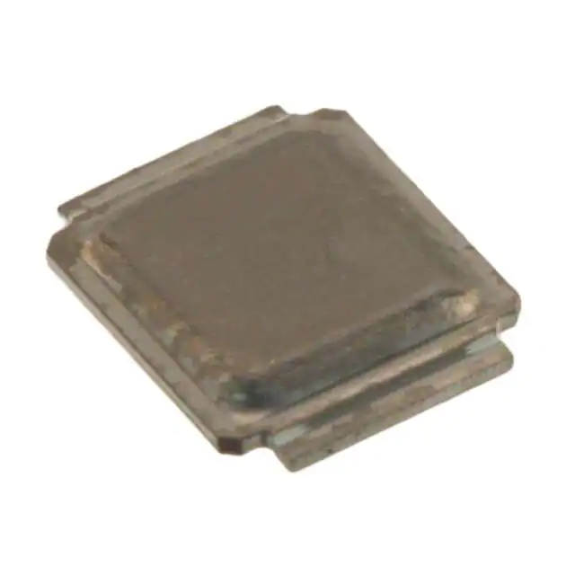
CanPAKTM M
MG-WDSON-2
• Dual sided cooling
• low parasitic inductance
• Low profile (2|I D|R DS(on)max,
I D=30 A
2)
Device on 40 mm x 40 mm x 1.5 mm epoxy PCB FR4 with 6 cm2 (one layer, 70 µm thick) copper area for drain
connection. PCB is vertical in still air.
3)
See figure 3 for more detailed information
Rev. 2.0
page 2
2014-04-17
�BSB028N06NN3 G
Parameter
Values
Symbol Conditions
Unit
min.
typ.
max.
-
8800
12000 pF
-
2100
2800
Dynamic characteristics
Input capacitance
C iss
V GS=0 V, V DS=30 V,
f =1 MHz
Output capacitance
C oss
Reverse transfer capacitance
Crss
-
64
-
Turn-on delay time
t d(on)
-
21
-
Rise time
tr
-
9
-
Turn-off delay time
t d(off)
-
38
-
Fall time
tf
-
6
-
Gate to source charge
Q gs
-
41
-
Gate to drain charge
Q gd
-
8
-
-
23
-
V DD=30 V, V GS=10 V,
I D=30 A, R G,ext=1.6 W
ns
Gate Charge Characteristics5)
V DD=30 V, I D=30 A,
V GS=0 to 10 V
nC
Switching charge
Q sw
Gate charge total
Qg
-
108
143
Gate plateau voltage
V plateau
-
4.6
-
Output charge
Q oss
-
87
116
-
-
30
-
-
120
-
0.8
1.2
V
-
60
-
ns
-
87
-
nC
V DD=30 V, V GS=0 V
V
Reverse Diode
Diode continuous forward current
IS
Diode pulse current
I S,pulse
Diode forward voltage
V SD
Reverse recovery time
t rr
A
T C=25 °C
V GS=0 V, I F=30 A,
T j=25 °C
V R=30 V, I F=I S,
di F/dt =100 A/µs
Reverse recovery charge
4)
5)
Q rr
See figure 13 for more detailed information
See figure 16 for gate charge parameter definition
Rev. 2.0
page 3
2014-04-17
�BSB028N06NN3 G
1 Power dissipation
2 Drain current
P tot=f(T C)
I D=f(T C); V GS≥10 V
90
100
80
90
80
70
70
60
ID [A]
Ptot [W]
60
50
40
50
40
30
30
20
20
10
10
0
0
0
25
50
75
100
125
150
175
0
25
TC [°C]
50
75
100
125
150
175
TC [°C]
3 Safe operating area
4 Max. transient thermal impedance
I D=f(V DS); T C=25 °C; D =0
Z thJC=f(t p)
parameter: t p
parameter: D =t p/T
103
101
limited by on-state
resistance
1 µs
10 µs
102
100 µs
100
1 ms
ZthJC [K/W]
101
ID [A]
10 ms
DC
100
0.5
0.2
0.1
10-1
10-1
0.05
0.02
0.01
single pulse
10-2
10-2
10-1
100
101
102
VDS [V]
Rev. 2.0
tp [s]
page 4
2014-04-17
�BSB028N06NN3 G
5 Typ. output characteristics
6 Typ. drain-source on resistance
I D=f(V DS); T j=25 °C
R DS(on)=f(I D); T j=25 °C
parameter: V GS
parameter: V GS
360
8
8V
10 V
7V
320
5V
280
5.5 V
6V
6
240
RDS(on) [mW]
ID [A]
6V
200
160
4
7V
5.5 V
8V
120
10V
2
80
5V
40
4.5V
0
0
0
1
2
3
0
40
80
120
VDS [V]
160
200
240
280
320
ID [A]
7 Typ. transfer characteristics
8 Typ. forward transconductance
I D=f(V GS); |V DS|>2|I D|R DS(on)max
g fs=f(I D); T j=25 °C
parameter: T j
200
160
160
120
ID [A]
gfs [S]
120
80
80
150 °C
40
25 °C
40
0
0
0
2
4
6
8
VGS [V]
Rev. 2.0
0
40
80
120
ID [A]
page 5
2014-04-17
�BSB028N06NN3 G
9 Drain-source on-state resistance
10 Typ. gate threshold voltage
R DS(on)=f(T j); I D=30 A; V GS=10 V
V GS(th)=f(T j); V GS=V DS
6
4
5
1020 µA
3
102 µA
VGS(th) [V]
RDS(on) [mW]
4
max
3
typ
2
2
1
1
0
0
-60
-20
20
60
100
140
180
-60
-20
20
Tj [°C]
60
100
140
180
Tj [°C]
11 Typ. capacitances
12 Forward characteristics of reverse diode
C =f(V DS); V GS=0 V; f =1 MHz
I F=f(V SD)
parameter: T j
104
100
Ciss
Coss
IF [A]
C [pF]
103
10
102
150 °C25 °C
Crss
101
25°C
150°C
98%98%
1
0
10
20
30
40
50
60
VDS [V]
Rev. 2.0
0.0
0.5
1.0
1.5
2.0
VSD [V]
page 6
2014-04-17
�BSB028N06NN3 G
13 Avalanche characteristics
14 Typ. gate charge
I AS=f(t AV); R GS=25 W
V GS=f(Q gate); I D=30 A pulsed
parameter: T j(start)
parameter: V DD
100
12
30 V
10
12V
48 V
125 °C
10
100 °C
VGS [V]
IAV [A]
8
25 °C
6
4
2
1
0
1
10
100
1000
10000
0
30
tAV [µs]
60
90
120
Qgate [nC]
15 Drain-source breakdown voltage
16 Gate charge waveforms
V BR(DSS)=f(T j); I D=1 mA
66
V GS
Qg
64
VBR(DSS) [V]
62
60
V gs(th)
58
56
Q g(th)
Q sw
Q gs
54
-60
-20
20
60
100
140
Q gate
Q gd
180
Tj [°C]
Rev. 2.0
page 7
2014-04-17
�BSB028N06NN3 G
Package Outline
Rev. 2.0
CanPAK™ M
MG-WDSON-2
page 8
2014-04-17
�BSB028N06NN3 G
CanPAK™ M
MG-WDSON-2
Dimensions in mm
Rev. 2.0
page 9
2014-04-17
�BSB028N06NN3 G
CanPAK™ M
MG-WDSON-2
Dimensions in mm
Raccomended stencil thikness 150 mm
Rev. 2.0
page 10
2014-04-17
�BSB028N06NN3 G
Published by
Infineon Technologies AG
81726 Munich, Germany
© 2011 Infineon Technologies AG
All Rights Reserved.
Legal Disclaimer
The information given in this document shall in no event be regarded as a guarantee of
conditions or characteristics. With respect to any examples or hints given herein, any typical
values stated herein and/or any information regarding the application of the device,
Infineon Technologies hereby disclaims any and all warranties and liabilities of any kind,
including without limitation, warranties of non-infringement of intellectual property rights
of any third party.
Information
For further information on technology, delivery terms and conditions and prices, please
contact the nearest Infineon Technologies Office (www.infineon.com).
Warnings
Due to technical requirements, components may contain dangerous substances. For information
on the types in question, please contact the nearest Infineon Technologies Office.
Infineon Technologies components may be used in life-support devices or systems only with
the express written approval of Infineon Technologies, if a failure of such components can
reasonably be expected to cause the failure of that life-support device or system or to affect
the safety or effectiveness of that device or system. Life support devices or systems are
intended to be implanted in the human body or to support and/or maintain and sustain
and/or protect human life. If they fail, it is reasonable to assume that the health of the user
or other persons may be endangered.
Rev. 2.0
page 11
2014-04-17
�
很抱歉,暂时无法提供与“BSB028N06NN3GXUMA1”相匹配的价格&库存,您可以联系我们找货
免费人工找货- 国内价格
- 1+16.10078
- 10+14.88381
- 25+13.85946
- 100+13.16780
- 250+12.83510
- 500+10.65506


 工商网监
湘ICP备2023018690号
工商网监
湘ICP备2023018690号
