BTS71040-4ESA
SPOC™ +2
4x 22.5 mΩ
Serial Interface Power Controller
1
Package
PG-TSDSO-24
Marking
71040-4ESA
Overview
Potential Applications
•
Suitable for resistive, inductive and capacitive loads
•
Replaces electromechanical relays, fuses and discrete circuits
•
Driving capability suitable for 3 A loads and high inrush current loads such
as 27W bulb or equivalent electronic loads (e.g. LED modules)
VBAT
Optional
ZWIRE
Fail-safe
Control
RIN
Optional
CVSGND
CVS1
Logic Supply
RGND
T1
CVDD
RIN
IN2
GPIO
RIN
IN3
RLHI
LHI
CSN
RCSN
CSN
SCLK
RSCLK
SCLK
RSO
RIS_PROT
CADC
DZ1
ROL
SI
IS
Logic GND
COUT
RSENSE
COUT
RADC
COUT
ADC
OUT2
OUT3
SO
RSI
MOSI
VSS
OUT0
OUT1
ZWIRE
GPIO
ZLOAD*
IN1
RPD
IN0
RIN
ZWIRE
RIN
GPIO
ZLOAD*
GPIO
MISO
VS
COUT
CVS2
Microcontroller
DZ2
GND
VDD
SPOC™ +2
RVDD
VDD
Optional
Application_4ch_noED.emf
Power GND
*See Chapter 1 „Potential Applications“
**See Chapter 11.2 „External Components“
Chassis GND
Figure 1
Data Sheet
Application Diagram. Further information in Chapter 11
www.infineon.com
1
Rev. 1.10
2021-03-23
�BTS71040-4ESA
SPOC™ +2
Overview
Basic Features
•
High-Side Switch with Diagnosis and Embedded Protection
•
Part of SPOC™ +2 Family
•
Daisy Chain capable SPI interface
•
3.3 V and 5 V compatible logic pins
•
Slew rate control for all Channels
•
ReverseON for low power dissipation in Reverse Polarity
•
Switch ON capability while Inverse Current condition (InverseON)
•
Green Product (RoHS compliant)
Protection Features
•
Absolute and dynamic temperature limitation with controlled restart
•
Overcurrent protection (tripping) with Programmable Restart Control and Current Threshold
•
Undervoltage shutdown
•
Overvoltage protection with external components
Diagnostic Features
•
Proportional load current sense multiplexed
•
Open Load in ON and OFF state
•
Short circuit to ground and battery
•
Diagnosis feedback via SPI
Functional Safety Features
•
Limp Home mode
•
Monitoring of Input pin status (IN and LHI)
•
Checksum verification of Configuration Registers
•
Current Sense verification mode
Product Validation
Qualified for automotive applications. Product validation according to AEC-Q100 Grade 1.
Description
The BTS71040-4ESA is a Serial Interface Power Controller, providing protection functions and diagnosis. The
device is integrated in SMART7 technology.
Data Sheet
2
Rev. 1.10
2021-03-23
�BTS71040-4ESA
SPOC™ +2
Overview
Table 1
Product Summary
Parameter
Symbol
Values
Minimum Operating voltage (at switch ON)
VS(OP)
4.1 V
Minimum Operating voltage (cranking)
VS(UV)
3.1 V
Maximum Operating voltage
VS
28 V
Digital Supply voltage
VDD
3.3 V or 5 V
Minimum Overvoltage protection (TJ ≥ 25 °C)
VDS(CLAMP)_25
35 V
Maximum current in Sleep mode (TJ ≤ 85 °C)
IVS(SLEEP)_85
0.4 µA
Maximum operative current
IGND(ACTIVE)
7 mA
Maximum ON-state resistance (TJ = 150 °C)
RDS(ON)_150
38 mΩ
Nominal load current (TA = 85 °C)
IL(NOM)
3A
Typical current sense ratio at IL = IL(NOM)
kILIS
2000
Serial Clock Frequency
fSCLK(max)
5 MHz
Data Sheet
3
Rev. 1.10
2021-03-23
�BTS71040-4ESA
SPOC™ +2
Block Diagram and Terms
2
Block Diagram and Terms
2.1
Block Diagram
VS
Channel 0
Channel 1
Channel 2
Channel 3
VDD
SO
Voltage Sensor
SI
Overtemp eratur e
SCLK
CSN
LHI
IN0
Driver
Logic
ESD
Protection
+
I/O Logic
Gat e Co ntrol
&
Chargepump
ReverseON
In verseON
T
Overvolt age
Clamping
OUT0
OUT1
Overcurr ent
Pr otec tion
OUT2
OUT3
Outp ut Voltage Limitation
IN1
IN2
Load Current Sense Mult iplexer
IN3
In ternal Power Sup ply
Overvolt age P rotection
IS
GND
Reverse Polarity
Pr otection
VS Mo nitoring
Limp Home Cont rol
GND Cir cuitr y
SPI Interface
In ternal Logic Supply
BlockDiagram_4chnoED.emf
Figure 2
Data Sheet
Block Diagram of BTS71040-4ESA
4
Rev. 1.10
2021-03-23
�BTS71040-4ESA
SPOC™ +2
Block Diagram and Terms
2.2
Terms
Figure 3 shows all terms used in this data sheet, with associated convention for positive values.
IVS
VSIS
VS
IDD
VDD
ISO
VS
VDSn
SO
SI
VDD
SCLK
VSO
ICSN
VSI
CSN
ILHI
VSCLK
OUTn
LHI
IINn
VCSN
VLHI
I Ln
INn
IIS
VOUTn
IS
GND
VINn
VIS
IGND
Terms_noED.emf
Figure 3
Data Sheet
Voltage and Current Convention
5
Rev. 1.10
2021-03-23
�BTS71040-4ESA
SPOC™ +2
Pin Configuration
3
Pin Configuration
3.1
Pin Assignment
(top view)
GND
VDD
SO
SI
SCLK
CSN
LHI
IN0
IN1
IN2
IN3
IS
1
2
3
4
5
6
VS
7
8
9
10
11
12
exposed pad (bottom)
24
23
22
21
20
19
18
17
16
15
14
13
n.c.
n.c.
OUT0
OUT0
OUT1
OUT1
OUT2
OUT2
OUT3
OUT3
n.c.
n.c.
PinOut_SPOC_040_noED.emf
Figure 4
Data Sheet
Pin Configuration
6
Rev. 1.10
2021-03-23
�BTS71040-4ESA
SPOC™ +2
Pin Configuration
3.2
Pin Definitions and Functions
Table 2
Pin Definition
Pin
Symbol
I/O
Function
EP
VS
(exposed pad)
-
Power Supply Voltage
Battery voltage
1
GND
-
Ground
2
VDD
-
Digital Supply Voltage
3
SO
O
Serial output of SPI interface
4
SI
I
Serial input of SPI interface (“high” active)
5
SCLK
I
Serial clock of SPI interface (“high” active)
6
CSN
I
Chip select of SPI interface (“low” active); integrated pull up to VDD
7
LHI
I
Limp Home activation signal (“high” active)
8, 9
10, 11
INn
I
Input Channel n
Digital signal to switch ON the channel n (“high” active)
If not used: connect with a 10 kΩ resistor either to GND pin or to module
ground
12
IS
O
Current sense output signal
23-24
n.c.
-
Not connected, internally not bonded, shorted together
21-22
19-20
17-18
15-16
OUTn
O
Output n
Protected high-side power output of channel n1)
13-14
n.c.
-
Not connected, internally not bonded, shorted together
1) All output pins of the channel must be connected together on the PCB. All pins of the output are internally connected
together. PCB traces have to be designed to withstand the maximum current which can flow.
Data Sheet
7
Rev. 1.10
2021-03-23
�BTS71040-4ESA
SPOC™ +2
General Product Characteristics
4
General Product Characteristics
4.1
Absolute Maximum Ratings - General
Table 3
Absolute Maximum Ratings1)
TJ = -40 °C to +150 °C; all voltages with respect to ground, positive current flowing into pin
(unless otherwise specified)
Parameter
Symbol
Values
Min.
Typ.
Max.
Unit
Note or
Number
Test Condition
Supply pins
Power Supply Voltage
VS
-0.3
–
28
V
–
P_4.1.0.1
Digital Supply Voltage
VDD
-0.3
–
5.5
V
–
P_4.1.0.29
Load Dump Voltage
VBAT(LD)
–
–
35
V
suppressed
Load Dump
acc. to
ISO16750-2
(2010).
Ri = 2 Ω
P_4.1.0.3
Supply Voltage for Short Circuit VBAT(SC)
Protection
0
–
24
V
Setup acc. to
AEC-Q100-012
P_4.1.0.25
Reverse Polarity Voltage
-VBAT(REV)
–
–
16
V
t ≤ 2 min
TA = +25 °C
Setup as
described in
Chapter 11
P_4.1.0.5
Current through GND Pin
IGND
-50
–
50
mA
RGND according P_4.1.0.9
to Chapter 11
Current through VDD Pin
IVDD(REV)
-10
–
30
mA
t ≤ 2 min
P_4.1.0.10
50
–
–
ms
–
P_4.1.0.35
Counter Reset Delay Time after tRETRY
Fault Condition
Logic & control pins (Digital Input = DI)
DI = INn, CS, SCLK, SI, LHI
Current through DI Pin
IDI
-1
–
2
mA
2)
P_4.1.0.14
Current through DI Pin
Reverse Battery Condition
IDI(REV)
-1
–
10
mA
2)
P_4.1.0.36
t ≤ 2 min
Logic & control pins (Digital Output = DO)
DO = SO
Current through DO Pin
IDO
-2
–
1
mA
2)
P_4.1.0.33
Current through DO Pin
Reverse Battery Condition
IDO(REV)
-10
–
1
mA
2)
P_4.1.0.37
Data Sheet
t ≤ 2 min
8
Rev. 1.10
2021-03-23
�BTS71040-4ESA
SPOC™ +2
General Product Characteristics
Table 3
Absolute Maximum Ratings1) (continued)
TJ = -40 °C to +150 °C; all voltages with respect to ground, positive current flowing into pin
(unless otherwise specified)
Parameter
Symbol
Values
Min.
Typ.
Max.
Unit
Note or
Number
Test Condition
V
IIS = 10 μA
P_4.1.0.16
–
P_4.1.0.18
IS pin
Voltage at IS Pin
VIS
-1.5
–
VS
Current through IS Pin
IIS
-25
–
IIS(SAT),M mA
AX
Temperatures
Junction Temperature
TJ
-40
–
150
°C
–
P_4.1.0.19
Storage Temperature
TSTG
-55
–
150
°C
–
P_4.1.0.20
ESD Susceptibility all Pins
(HBM)
VESD(HBM)
-2
–
2
kV
HBM3)
P_4.1.0.21
ESD Susceptibility OUTn vs
GND and VS connected (HBM)
VESD(HBM)_OUT -4
–
4
kV
HBM3)
P_4.1.0.22
ESD Susceptibility all Pins
(CDM)
VESD(CDM)
-500
–
500
V
CDM4)
P_4.1.0.23
ESD Susceptibility Corner Pins VESD(CDM)_CRN -750
(pins 1, 12, 13, 24)
–
750
V
CDM4)
P_4.1.0.24
ESD Susceptibility
1)
2)
3)
4)
Not subject to production test - specified by design.
Maximum VDI to be considered for Latch-Up tests: 5.5 V.
ESD susceptibility, Human Body Model "HBM", according to AEC Q100-002.
ESD susceptibility, Charged Device Model "CDM", according to AEC Q100-011.
Notes
1. Stresses above the ones listed here may cause permanent damage to the device. Exposure to absolute
maximum rating conditions for extended periods may affect device reliability.
2. Integrated protection functions are designed to prevent IC destruction under fault conditions described in the
data sheet. Fault conditions are considered as “outside” normal operating range. Protection functions are
not designed for continuous repetitive operation.
Data Sheet
9
Rev. 1.10
2021-03-23
�BTS71040-4ESA
SPOC™ +2
General Product Characteristics
4.2
Absolute Maximum Ratings - Power Stages
4.2.1
Power Stages - 22.5 mΩ channels
Table 4
Absolute Maximum Ratings - 22.5 mΩ channels1)
TJ = -40 °C to +150 °C; all voltages with respect to ground, positive current flowing into pin
(unless otherwise specified)
Parameter
Symbol
Values
Min.
Typ.
Max.
Unit
Note or
Test Condition
Number
Maximum Energy Dissipation
Single Pulse
EAS
–
–
28
mJ
IL = 2*IL(NOM)
TJ(0) = 150 °C
VS = 28 V
P_4.2.16.1
Maximum Energy Dissipation
Repetitive Pulse
EAR
–
–
8.5
mJ
IL = IL(NOM)
TJ(0) = 85 °C
VS = 13.5 V
1M cycles
P_4.2.16.2
Load Current
|IL|
–
–
IL(OVL),MAX A
–
P_4.2.16.3
1) Not subject to production test - specified by design.
Data Sheet
10
Rev. 1.10
2021-03-23
�BTS71040-4ESA
SPOC™ +2
General Product Characteristics
4.3
Functional Range
Table 5
Functional Range - Supply Voltages and Temperature1)
Parameter
Symbol
Values
Unit
Note or
Test Condition
Number
Min.
Typ.
Max.
Power Supply Voltage
VS(NOR)
Range for Normal Operation
6
13.5
18
V
–
P_4.3.0.1
Lower Extended Power
Supply Voltage Range for
Operation
VS(EXT,LOW)
3.1
–
6
V
2)3)
P_4.3.0.2
Upper Extended Power
Supply Voltage Range for
Operation
VS(EXT,UP)
18
Digital Supply Voltage
Range
VDD(NOR)
3.0
–
5.5
V
–
P_4.3.0.4
Junction Temperature
TJ
-40
–
150
°C
–
P_4.3.0.5
(parameter
deviations possible)
–
28
V
3)
P_4.3.0.3
(parameter
deviations possible)
1) Not subject to production test - specified by design.
2) In case of VS voltage decreasing: VS(EXT,LOW),MIN = 3.1 V. In case of VS voltage increasing: VS(EXT,LOW),MIN = 4.1 V.
3) Protection functions still operative.
Note:
Within the functional or operating range, the IC operates as described in the circuit description. The
electrical characteristics are specified within the conditions given in the Electrical Characteristics
tables.
4.4
Thermal Resistance
Note:
This thermal data was generated in accordance with JEDEC JESD51 standards. For more
information, go to www.jedec.org.
Table 6
Thermal Resistance1)
Parameter
Symbol
Values
Min.
Typ.
Max.
Unit
Note or
Test Condition
Number
Thermal Characterization
Parameter Junction-Top
ΨJTOP
–
0.9
1.5
K/W
2)
P_4.4.0.17
Thermal Resistance
Junction-to-Case
RthJC
–
0.5
0.9
K/W
2)
P_4.4.0.18
Thermal Resistance
Junction to Ambient
RthJA
–
simulated at
exposed pad
26.5
–
K/W
2)
P_4.4.0.10
1) Not subject to production test - specified by design.
2) According to Jedec JESD51-2,-5,-7 at natural convection on FR4 2s2p board; the Product (Chip + Package) was
simulated on a 76.2 × 114.3 × 1.5 mm board with 2 inner copper layers (2 × 70 µm Cu, 2 × 35 µm Cu). Where applicable
a thermal via array under the exposed pad contacted the first inner copper layer. Simulation done at TA = 105°C,
PDISSIPATION = 1 W.
Data Sheet
11
Rev. 1.10
2021-03-23
�BTS71040-4ESA
SPOC™ +2
General Product Characteristics
4.4.1
PCB Setup
1,5 mm
70 µm modeled (traces, cooling area)
70 µm, 5% metalization*
*: means percentual Cu metalization on each layer
PCB_Zth_1s0p.emf
Figure 5
1s0p PCB Cross Section
70 µm modeled (traces)
1,5 mm
35 µm, 90% metalization*
35 µm, 90% metalization*
70 µm, 5% metalization*
*: means percentual Cu metalization on each layer
PCB_Zth_2s2p.emf
Figure 6
2s2p PCB Cross Section
PCB 1s0p + 600 mm2 cooling
PCB 2s2p / 1s0p footprint
PCB_sim_setup_TSDSO24.emf
Figure 7
PCB setup for thermal simulations
PCB_2s2p_vias_TSDSO24.emf
Figure 8
Data Sheet
Thermal vias on PCB for 2s2p PCB setup
12
Rev. 1.10
2021-03-23
�BTS71040-4ESA
SPOC™ +2
General Product Characteristics
4.4.2
Thermal Impedance
BTS71040-4ESx
100
ZthJA [K/W]
TAMBIENT = 105 °C
10
1
0.1
2s2p
1s0p - 600 mm²
1s0p - 300 mm²
1s0p - footprint
0.01
0.0001
0.001
0.01
0.1
1
10
100
1000
Time [s]
Figure 9
Typical Thermal Impedance. PCB setup according Chapter 4.4.1
BTS71040-4ESx
90
1s0p - Ta = 105 °C
80
RthJA [K/W]
70
60
50
40
30
0
100
200
300
400
500
600
Cooling area [mm²]
Figure 10
Data Sheet
Thermal Resistance on 1s0p PCB with various cooling surfaces
13
Rev. 1.10
2021-03-23
�BTS71040-4ESA
SPOC™ +2
Logic Pins
5
Logic Pins
The device has 9 digital pins to configure and control the device. They can be grouped based on their function
into input pins, SPI pins and Limp Home pin.
5.1
Input Pins (INn)
The input pins IN0 to IN3 activate the corresponding output channel, if the device is either in Sleep, Stand-by,
Ready or in Limp Home mode. The input circuitry is compatible with 3.3V and 5V microcontroller. The
electrical equivalent of the input circuitry is shown in Figure 11. In case the pin is not used, it must be
connected with a 10 kΩ resistor either to GND pin or to module ground.
VS
IN
VS(CLAMP)
IDI
ESD
IDI
VDI(CLAMP)
VDI
IGND
RGND
GND
Input_IN_INTDIO.emf
Figure 11
Input circuitry
The logic thresholds for “low” and “high” states are defined by parameters VDI(TH) and VDI(HYS). The relationship
between these two values is shown in Figure 12. The voltage VIN needed to ensure a “high” state is always
higher than the voltage needed to ensure a “low” state.
Data Sheet
14
Rev. 1.10
2021-03-23
�BTS71040-4ESA
SPOC™ +2
Logic Pins
V DI
V DI(TH ),M AX
V DI(TH)
V DI(HYS)
V DI(TH ),M IN
t
Internal channel
activation signal
0
x
1
x
0
t
Input_VDITH_2.emf
Figure 12
Input Threshold voltages and hysteresis
There are two ways of using the input pins in combination with the register OUT by programming bit
HWCR.COL in register HWCR (see Table 30).
•
HWCR.COL = 0B: A channel is switched ON either by the according OUT.OUTn bit or by the input pin.
•
HWCR.COL = 1B: A channel is switched ON by the according OUT.OUTn bit only, when the input pin is
“high”. In this configuration, a PWM signal can be applied to the input pin and the channel is activated by
the SPI register OUT (see Table 30).
The default state (HWCR.COL = 0B) is the OR-combination of the input signal and the SPI-bit. In Limp Home
mode (LHI pin set to “high”) the combinatorial logic is in default state to enable a channel activation via the
input pins only. Figure 13 shows the complete input switch matrix.
The logic level of the input pins can be monitored via the input status monitor. In case of a “high” level on an
input pin, the corresponding ICS.INSTn bit is set and cleared on read.
Data Sheet
15
Rev. 1.10
2021-03-23
�BTS71040-4ESA
SPOC™ +2
Logic Pins
MUX≠111 OUT2
OUT1
&
OUT3
&
OUT0
&
PCC0
&
OR
IN0
IIN 0
&
Gate Control 0
OR
Gate Control 3
OR
IN3
IIN 1
&
OR
IN1
IIN 2
&
Gate Control 1
OR
Gate Control 2
OR
IN2
IIN 3
&
COL
PCC1
LogicPins_InputMatrix_4chnoED_PCC.emf
Figure 13
Input Switch Matrix
5.2
Advanced Features Pins
5.2.1
SPI Pins
The serial peripheral interface (SPI) is a full duplex synchronous serial slave interface, which uses four lines:
SO, SI, SCLK and CSN. See Chapter 10 for further information.
5.2.2
Limp Home Input (LHI) Pin
For activating the fail-safe state, the device features a Limp Home Input pin. When the pin is set to “high” for
a time longer than tLHI(AC), the Limp Home mode will be activated. See Chapter 6.1.7 and Chapter 6.1.8 for
further information.
Data Sheet
16
Rev. 1.10
2021-03-23
�BTS71040-4ESA
SPOC™ +2
Logic Pins
5.3
Electrical Characteristics Logic Pins
VDD = 3.0 V to 5.5 V, VS = 6 V to 18 V, TJ = -40 °C to +150 °C
Typical values: VDD = 5.0 V, VS = 13.5 V, TJ = 25 °C
Digital Input (DI) pins = IN
Table 7
Electrical Characteristics: Logic Pins - General
Parameter
Symbol
Values
Min.
Typ.
Max.
Unit
Note or
Test Condition
Number
Digital Input Voltage
Threshold
VDI(TH)
0.8
1.3
2
V
See Figure 11 and P_5.4.0.1
Figure 12
Digital Input Clamping
Voltage
VDI(CLAMP1)
–
7
–
V
1)
Digital Input Clamping
Voltage
VDI(CLAMP2)
6.5
7.5
8.5
V
IDI = 2 mA
P_5.4.0.3
See Figure 11 and
Figure 12
Digital Input Hysteresis
VDI(HYS)
–
0.25
–
V
1)
IDI(H)
2
10
25
µA
VDI = 2 V
P_5.4.0.5
See Figure 11 and
Figure 12
Digital Input Current (“low”) IDI(L)
2
10
25
µA
VDI = 0.8 V
P_5.4.0.6
See Figure 11 and
Figure 12
Digital Input Current
(“high”)
P_5.4.0.2
IDI = 1 mA
See Figure 11 and
Figure 12
P_5.4.0.4
See Figure 11 and
Figure 12
1) Not subject to production test - specified by design.
5.4
Electrical Characteristics Logic Pins - Advanced Features
Table 8
Electrical Characteristics: Logic Pins - Advanced
Parameter
Symbol
Values
Min.
Typ.
Max.
Unit Note or
Number
Test Condition
SPI pins
Digital Input Voltage
Threshold of Pin CSN
VCSN(TH)
0.8
1.3
2
V
–
P_5.5.0.1
Digital Input Voltage
Threshold of Pin SCLK
VSCLK(TH)
0.8
1.3
2
V
1)
P_5.5.0.2
Digital Input Voltage
Threshold of Pin SI
VSI(TH)
0.8
1.3
2
V
–
P_5.5.0.3
Digital Input Clamping
Voltage of Pin CSN
VCSN(CLAMP1)
–
7
–
V
2)
P_5.5.0.4
Digital Input Clamping
Voltage of Pin CSN
VCSN(CLAMP2)
6.5
Data Sheet
ICSN = 1 mA
7.5
17
8.5
V
ICSN = 2 mA
P_5.5.0.5
Rev. 1.10
2021-03-23
�BTS71040-4ESA
SPOC™ +2
Logic Pins
Table 8
Electrical Characteristics: Logic Pins - Advanced (continued)
Parameter
Symbol
Values
Min.
Typ.
Max.
Unit Note or
Number
Test Condition
7
–
V
2)
Digital Input Clamping
Voltage of Pin SCLK
VSCLK(CLAMP1)
–
Digital Input Clamping
Voltage of Pin SCLK
VSCLK(CLAMP2)
6.5
7.5
8.5
V
ISCLK = 2 mA
P_5.5.0.7
Digital Input Clamping
Voltage of Pin SI
VSI(CLAMP1)
–
7
–
V
2)
P_5.5.0.8
Digital Input Clamping
Voltage of Pin SI
VSI(CLAMP2)
6.5
7.5
8.5
V
ISI = 2 mA
P_5.5.0.9
Digital Input Hysteresis of
Pin CSN
VCSN(HYS)
–
0.25
–
V
2)
P_5.5.0.11
Digital Input Hysteresis of
Pin SCLK
VSCLK(HYS)
–
Digital Input Hysteresis of
Pin SI
VSI(HYS)
–
Digital Input Current
(“low”) of Pin CSN
-ICSN(L)
2
10
25
μA
VCSN = 0.5 V
P_5.5.0.10
Digital Input Current
(“high”) of Pin CSN
-ICSN(H)
2
10
25
μA
VCSN = 2.6 V
P_5.5.0.12
Digital Input Current
(“low”) of Pin SCLK
ISCLK(L)
2
10
25
μA
VSCLK = 0.5 V
P_5.5.0.14
Digital Input Current
(“high”) of Pin SCLK
ISCLK(H)
2
10
25
μA
VSCLK = 2.6 V
P_5.5.0.16
Digital Input Current
(“low”) of Pin SI
ISI(L)
2
10
25
μA
VSI = 0.5 V
P_5.5.0.18
Digital Input Current
(“high”) of Pin SI
ISI(H)
2
10
25
μA
VSI = 2.6 V
P_5.5.0.20
Digital Output Voltage
(“low”) of Pin SO
VSO(L)
0
–
0.5
V
ISO = -0.5 mA
P_5.5.0.22
Digital Output Voltage
(“high”) of Pin SO
VSO(H)
VDD 0.5 V
–
VDD
V
ISO = 0.5 mA
P_5.5.0.23
Output Tristate Leakage
Current of Pin SO
ISO(OFF)
-1
–
1
μA
VCSN = VDD
VSO = 0 V or
VCSN = VDD
VSO = VDD
P_5.5.0.24
Digital Input Voltage
Threshold of Pin LHI
VLHI(TH)
1.4
1.9
2.6
V
–
P_5.5.0.25
Digital Input Clamping
Voltage of Pin LHI
VLHI(CLAMP1)
–
7
–
V
2)
P_5.5.0.27
Digital Input Clamping
Voltage of Pin LHI
VLHI(CLAMP2)
6.5
P_5.5.0.6
ISCLK = 1 mA
ISI = 1 mA
See Figure 12
0.25
–
V
2)
P_5.5.0.13
See Figure 12
0.25
–
V
2)
P_5.5.0.15
See Figure 12
LHI pin
Data Sheet
ILHI = 1 mA
7.5
18
8.5
V
ILHI = 2 mA
P_5.5.0.28
Rev. 1.10
2021-03-23
�BTS71040-4ESA
SPOC™ +2
Logic Pins
Table 8
Electrical Characteristics: Logic Pins - Advanced (continued)
Parameter
Symbol
Values
Min.
Typ.
Max.
Unit Note or
Number
Test Condition
Digital Input Hysteresis of
Pin LHI
VLHI(HYS)
–
0.25
–
V
2)
P_5.5.0.29
Digital Input Current
(“high”) of Pin LHI
ILHI(H)
10
32
65
µA
VLHI = 5 V
VDD = 0 V
P_5.5.0.30
Digital Input Current
(“low”) of Pin LHI
ILHI(L)
10
24
45
µA
VLHI = 0.8 V
VDD = 0 V
P_5.5.0.32
1) Functional test only.
2) Not subject to production test - specified by design.
Data Sheet
19
Rev. 1.10
2021-03-23
�BTS71040-4ESA
SPOC™ +2
Power Supply
6
Power Supply
The BTS71040-4ESA is supplied by two supply voltages:
•
Power Supply Voltage (VS)
•
Digital Supply Voltage (VDD)
The VS supply line is connected to a battery feed and used for the driving circuitry of the power stages, while
VDD is used for the SPI logic and for driving SO pin. VS and VDD supply voltages have an undervoltage detection
circuit, which prevents the activation of the associated function in case the measured voltage is below the
undervoltage threshold. More in detail:
•
An undervoltage on VDD supply prevents SPI communication. SPI registers are reset to their default values
•
An undervoltage on VS supply switches OFF all channels, even in Limp Home mode. The channels are
enabled again as soon as VS ≥ VS(OP)
The voltage at pin VS is also monitored. In case of a negative voltage transient on VS resulting in VS < VS(TP) when
the device is out of Sleep mode, any SPI command sent by the microcontroller is not accepted (see
Chapter 6.2 and Chapter 10.5 for further information). An overview of channel behavior according to
different VS and VDD supply voltages is shown in Table 9.
Table 9
Device capability as function of VS and VDD1)
VS ≤ VS(TP)
(VS(TP) see P_6.4.0.5)
VS(TP) < VS ≤ VS(UV)
(VS(UV) see P_6.4.0.1)
VS > VS(UV)3)
VDD ≤ VDD(PO)
(VDD(PO) see P_6.4.1.1)
VDD > VDD(PO)
Channels are OFF
Channels are OFF
SPI registers reset
SPI registers protected
SPI communication not available
(fSCLK = 0 MHz)
SPI communication available2)
(fSCLK = 5 MHz)
Limp Home mode not available
Limp Home mode not available
Channels are OFF
Channels are OFF
SPI registers reset
SPI registers available
SPI communication not available
(fSCLK = 0 MHz)
SPI communication available
(fSCLK = 5 MHz)
Limp Home mode available
(channels are OFF)
Limp Home mode available
(channels are OFF)
Channels cannot be controlled by SPI
Channels can be controlled by SPI
SPI registers reset
SPI registers available
SPI communication not available
(fSCLK = 0 MHz)
SPI communication available
(fSCLK = 5 MHz)
Limp Home mode available
Limp Home mode available
1) Valid after a successful supply voltage ramp-up.
2) Write commands are ignored. Furthermore the device responds with STDDIAG only.
3) The undervoltage condition on VS supply must be considered. See Chapter 6.2.
Data Sheet
20
Rev. 1.10
2021-03-23
�BTS71040-4ESA
SPOC™ +2
Power Supply
6.1
Operation Modes
BTS71040-4ESA has the following operation modes:
•
Sleep mode
•
Active mode
•
Stand-by mode
•
Ready mode
•
Limp Home mode
•
Limp Home Active mode
The transition between operation modes is determined according to these variables:
•
Digital supply level (VDD)
•
Logic level at INn pins
•
Logic level at LHI pin
•
Current sense multiplexer state (DCR.MUX)
•
Output register state (OUT.OUTn)
•
Configuration registers state
The state diagram including the possible transitions is shown in Figure 14. The behavior of BTS71040-4ESA as
well as some parameters may change in dependence from the operation mode of the device. Furthermore,
due to the undervoltage detection circuitry which monitors VS supply voltage, some changes within the same
operation mode can be seen accordingly.
There are five parameters describing each operation mode of BTS71040-4ESA:
•
Status of the output channels
•
Status of SPI registers
•
Status of SPI communication
•
Current consumption at VS pin (measured by IVS in Sleep mode, IGND in all other operative modes)
•
Current consumption at VDD pin (IVDD)
Table 10 shows the correlation between operation modes, VS and VDD supply voltages, and the state of the
most important functions (channel status, SPI communication and SPI registers).
Data Sheet
21
Rev. 1.10
2021-03-23
�BTS71040-4ESA
SPOC™ +2
Power Supply
LHI = "high"
Unsupplied
Stand-by
DCR.MUX = 111B or SPI_Reset
Power-up
LHI = "low"
Sleep
LHI = "high"
DCR.MUX ≠ 111B
OUT.OUTn = 1B
or INn = "high"
INn = "low" or INn = "low" & SPI_Reset
INn = "low" &
OUT.OUTn = 0B
OUT.OUTn = 0B or
SPI_Reset
INn = "high"
Limp Home
OUT.OUTn = 1B
DCR.MUX ≠ 111B or INn = "high"
Active
Ready
DCR.MUX = 111B & INn = "low"
LHI = "high"
INn = "low"
LHI = "high" & INn = "low"
INn = "high"
Limp Home
Active
LHI = "high" & INn = "high"
LHI = "low" & INn = "high"
Note: SPI bits which are not stated are considered to have the default value or are unchanged compared to the previous state. Supply voltages are
considered to be in operative range if not specified different. SPI_Reset is performed if VDD < VDD(PO) or HWCR.RST = 1B
Dashed lines indicate transitions between modes which should not be used for normal operation.
PowerSuppl y_OpModes.emf
Figure 14
Operation Mode state diagram
Table 10
Device function in relation to operation modes, VDD and VS voltages
Operative Mode Function
VS ≤ VS(TP)
VS(TP) ≤ VS ≤ VS(UV)
VS > VS(UV)
Sleep
OFF
OFF
OFF
SPI registers available1)
available1)
available1)
SPI comm.
available1)
available1)
available1)
Channels
OFF
OFF
OFF
Stand-by
Channels
1)
1)
available1)
SPI comm.
all commands rejected1) available1)
available1)
Channels
OFF
OFF
SPI registers protected
Ready
available
OFF
1)
1)
available1)
SPI comm.
all commands rejected1) available1)
available1)
Channels
OFF
OFF
follow SPI and/or Input
pins
available1)
available1)
SPI comm.
all commands rejected1) available1)
available1)
Channels
OFF
OFF
follow Input pins
SPI registers protected1)
reset
(Diagnosis available)1)
reset
(Diagnosis available)1)
SPI comm.
read-only1)
read-only1)
SPI registers protected
Active
available
SPI registers protected1)
Limp Home /
Limp Home
Active
all commands
rejected1)2)
1) In case VDD > VDD(PO) otherwise not available or in reset.
2) In case all input pins are set to “low”, SPI communication is in read-only mode.
Data Sheet
22
Rev. 1.10
2021-03-23
�BTS71040-4ESA
SPOC™ +2
Power Supply
6.1.1
Unsupplied
In this state, the device is either unsupplied (no voltage applied to VS pin and VDD pin) or the supply voltages
are both below the corresponding undervoltage threshold.
6.1.2
Power-up
The Power-up condition is entered when one of the supply voltages (VS or VDD) is applied to the device. Both
supplies are rising until they are above the undervoltage thresholds VS(OP) and VDD(PO) therefore the internal
Power-On signals are set. The SPI interface can be accessed after wake up time tWU(PO).
6.1.3
Sleep mode
The device is in Sleep mode when all Digital Input pins (INn, LHI) are set to “low” and DCR.MUX is still set to
111B. When BTS71040-4ESA is in Sleep mode, all outputs are OFF. The SPI registers can be programmed if VDD
> VDD(PO). The current consumption is minimum (see parameter IVS(SLEEP)). No Overtemperature or Overload
protection mechanism is active when the device is in Sleep mode. The circuitry that monitors VS versus VS(UV)
and VS versus VS(TP) is disabled. This allows the programming of the registers even if VS < VS(TP).
6.1.4
Stand-by mode
The device is in Stand-by mode when DCR.MUX ≠ 111B and no command to switch ON a channel was received
(either via SPI or via Input pins). All channels are OFF but the internal supply circuitry is working and therefore
the device current consumption is increased. A command to switch ON one or more outputs is accepted and
executed, bringing the device into Active mode. SPI communication is possible.
6.1.5
Ready mode
In Ready mode, one or more outputs received a command to switch ON (either via SPI or via Input pins if
HWCR.COL = 1B). Nevertheless, all outputs are OFF because of DCR.MUX bits still set to 111B. It is necessary
to change the value of those bits to bring the device into Active mode and switch ON the channels.
Note:
Since OUT register is blanked with DCR.MUX = 111B it is not possible to enter Active mode when
HWCR.COL bit is set to 1B.
6.1.6
Active mode
Active mode is the normal operation mode of BTS71040-4ESA when no Limp Home condition is set and one or
more outputs are switched ON. Device current consumption is specified by parameter IGND(ACTIVE). An
undervoltage condition on VDD supply voltage brings the device into Sleep mode in case all Input pins are set
to “low”.
6.1.7
Limp Home mode
The device enters Limp Home mode when LHI pin is set to “high” for t > tLHI(AC). SPI registers are reset to the
default values when Limp Home mode is entered. The corresponding bit in the standard diagnosis
(STDDIAG.LHI) will be set to 1B once the LHI pin is set to “high” and latched until next STDDIAG
transmission. See Figure 15 for further information. SPI registers are available for read access. ERRDIAG,
STDDIAG, WRNDIAG and ICS can be used for diagnosis in Limp Home.
When the device is in transient protection (VS ≤ VS(TP)) and the LHI pin is set to "high", the STDDIAG.LHI bit
will be set but the device will not change its state to Limp Home mode. Furthermore STDDIAG.VSMON and
STDDIAG.TER bits will be set to report the battery transient protection.
Data Sheet
23
Rev. 1.10
2021-03-23
�BTS71040-4ESA
SPOC™ +2
Power Supply
VS
VS(TP)
t
LHI
pin
t < tLHI(AC )
t
STDDIAG
.LHI
Read STDDIAG
SPI
tLHI(AC )
Read STDDIAG
tLH I(AC )
Read STDDIAG
tLHI(AC )
comm.
available
read-only
available
all command rejected
registers
available
reset
available
protected
Note: Device out o f Sleep mode when SPI comm. „available“
Figure 15
Limp Home Activation as function of VS
6.1.8
Limp Home Active mode
t
t
PowerSupply_LimpHomeActiv e.emf
Limp Home Active mode is entered when the device is in Limp Home mode and one of the IN pins is set to
“high”. Overload, Overtemperature and Overvoltage protections are active. Since SPI registers cannot be
written current sensing is not available.
Data Sheet
24
Rev. 1.10
2021-03-23
�BTS71040-4ESA
SPOC™ +2
Power Supply
6.1.9
Definition of Operation modes transition times
The channel turn-ON time is as defined by parameter tON when BTS71040-4ESA is in Active mode or in Limp
Home mode. In all other cases, it is necessary to add the transition time required to reach one of the two
aforementioned operation modes (as shown in Figure 16).
tLHI(AC)
tTRANS2STBY
tON + tTRANS2STBY
tOFF + tTRANS2SLP
Active
tON + tTRANS2STBY
tOFF + tTRANS2SLP
tLHI(AC) + tTRANS2STBY
Ready
Limp Home
tLHI(AC) + tTRANS2STBY
tOFF + tLHI(AC)
tLHI(AC)
tLHI(AC)
tOFF
tOFF
tLHI(AC) + tTRANS2SLP
Sleep
tON
tON
tTRANS2SLP
1 SPI frame
Stand-by
tWU(PO)
1 SPI frame
Unsupplied
Limp Home
Active
Note: Dashed lines indicate transition timings between modes which should not be used for normal operation.
PowerSuppl y_OpModes_Ti mings.emf
Figure 16
Transition Time diagram
6.2
Undervoltage on VS
Between VS(OP) and VS(UV) the undervoltage mechanism is triggered. If the device is operative (in Active or Limp
Home Active mode) and the supply voltage drops below the undervoltage threshold VS(UV), the internal logic
switches OFF the output channels. When the device is either in Stand-by, Active or Limp Home mode the bit
STDDIAG.VSMON is set and latched until readout. When the state is changed from Sleep to any other state,
a delay of t ≥ tTRANS2STBY has to be considered until STDDIAG.VSMON is valid.
As soon as the supply voltage VS is above the operative threshold VS(OP), the channels having the corresponding
input pin set to “high” or the bit in the OUT register set to 1B are switched ON again. The restart is delayed with
a time tDELAY(UV) which protects the device in case the undervoltage condition is caused by a short circuit event
(according to AEC-Q100-012), as shown in Figure 17.
Data Sheet
25
Rev. 1.10
2021-03-23
�BTS71040-4ESA
SPOC™ +2
Power Supply
VS
VS(O P)
VS(UV )
VS(HY S)
VS(TP)
t
tDEL AY(UV )
VO UT
t
STDDIAG.
VSMON
Read STDDIAG
t
Read STDDIAG
STDDIAG.
TER
Read STDDIAG
Opera tion
Mode
Stand-by
t
Read STDDIAG
Active
Sleep
Ready
Active
t
PowerSupply_UVRVS.emf
Figure 17
VS undervoltage behavior
6.3
Reset Condition
One of the following conditions reset the SPI registers to their default value:
•
VDD is not present or below the undervoltage threshold VDD(PO)
– SPI registers will be reset to their default values (in the first communication after reset the
STDDIAG.TER will be set to 1B).
– Restart counters will not be reset if VS is available or LHI is "high".
•
LHI pin is set to “high” for t > tLHI(AC) and VS > VS(TP)
– Configuration registers will be reset to their default values. ERRDIAG and WRNDIAG will be reset.
– Restart counters will be reset.
•
Reset command (HWCR.RST = 1B) is executed and VS > VS(TP)
– Configuration registers will be reset to their default values. ERRDIAG, WRNDIAG and STDDIAG will not
be reset.
– Restart counters will not be reset.
In case all Input pins are set to “low” after any reset condition, all channels are switched OFF.
Data Sheet
26
Rev. 1.10
2021-03-23
�BTS71040-4ESA
SPOC™ +2
Power Supply
6.4
Electrical Characteristics Power Supply
VDD = 3.0 V to 5.5 V, VS = 6 V to 18 V, TJ = -40 °C to +150 °C
Typical values: VDD = 5.0 V, VS = 13.5 V, TJ = 25 °C
Typical resistive loads connected to the outputs for testing (unless otherwise specified):
22.5 mΩ: RL = 4.8 Ω
Table 11
Electrical Characteristics: Power Supply - General
Parameter
Symbol
Values
Unit
Note or
Test Condition
Number
Min.
Typ.
Max.
Power Supply Undervoltage VS(UV)
Shutdown
1.8
2.3
3.1
V
VS decreasing
IN = “high” or
OUT.OUTn = 1B
From VDS ≤ 0.5 V to
VDS = VS
See Figure 17
P_6.4.0.1
Power Supply Minimum
Operating Voltage
VS(OP)
2.0
3.0
4.1
V
VS increasing
IN = “high”or
OUT.OUTn = 1B
From VDS = VS to
VDS ≤ 0.5 V
See Figure 17
P_6.4.0.3
Power Supply Voltage
Threshold for Battery
Transients Protection
VS(TP)
0.6
1.0
1.8
V
P_6.4.0.5
VS decreasing
STDDIAG.VSMON = 1B
STDDIAG.TER = 1B
DCR.MUX ≠111B
See Figure 17
Power Supply Undervoltage VS(HYS)
Shutdown Hysteresis
–
0.7
–
V
1)
Power Supply Undervoltage tDELAY(UV)
Recovery Time
2.5
Breakdown Voltage
-VS(REV)
between GND and VS Pins in
Reverse Battery
16
VS pin
P_6.4.0.6
VS(OP) - VS(UV)
See Figure 17
4
5.5
ms
1)
P_6.4.0.10
dVS/dt ≤ 0.5 V/µs
VS ≥ 0 V
See Figure 17
–
30
V
1)
P_6.4.0.9
IGND(REV) = 14 mA
TJ = 150 °C
1) Not subject to production test - specified by design.
Data Sheet
27
Rev. 1.10
2021-03-23
�BTS71040-4ESA
SPOC™ +2
Power Supply
6.4.1
Electrical Characteristics Power Supply - SPOC™
Table 12
Electrical Characteristics: Power Supply - SPOC™
Parameter
Symbol
Values
Min.
Typ.
Max.
4.3
5.5
Unit
Note or
Test Condition
Number
V
1)
P_6.4.1.1
VDD pin
Digital Supply Operating
Voltage
VDD(OP)
2.45
Digital Supply Power-On
Reset Threshold Voltage
VDD(PO)
1.4
Digital Supply Undervoltage VDD(UV)
Shutdown
1.3
1.8
2.2
V
VDD decreasing
P_6.4.1.2
OUT.OUTn = 1B
From VDS ≤ 0.5 V to
VDS = VS
Digital Supply Undervoltage VDD(HYS)
Shutdown Hysteresis
–
0.1
–
V
1)
P_6.4.1.3
Digital Supply Clamping
Voltage
VDD(CLAMP1)
–
6.5
–
V
1)
P_6.4.1.11
Digital Supply Clamping
Voltage
VDD(CLAMP2)
6
7
8
V
IDD = 20 mA
P_6.4.1.12
Power-On Wake Up Time
tWU(PO)
–
10
30
μs
1)
P_6.4.1.13
P_6.4.1.4
fSCLK = 5 MHz
1.9
2.3
V
1)
P_6.4.1.9
VDD increasing
IDD = 1 mA
Transition Time to Stand-by tTRANS2STBY
Mode
5
10
30
μs
1)
Transition Time to Sleep
Mode
tTRANS2SLP
1
5
60
μs
1)2)
P_6.4.1.5
Limp Home
Acknowledgement Time
tLHI(AC)
10
20
40
µs
1)
P_6.4.1.6
1) Not subject to production test - specified by design.
2) If output channel enters inductive clamping, clamping time has to be added.
Data Sheet
28
Rev. 1.10
2021-03-23
�BTS71040-4ESA
SPOC™ +2
Power Supply
6.5
Electrical Characteristics Power Supply - Product Specific
VDD = 3.0 V to 5.5 V, VS = 6 V to 18 V, TJ = -40 °C to +150 °C
Typical values: VDD = 5.0 V, VS = 13.5 V, TJ = 25 °C
Typical resistive loads connected to the outputs for testing (unless otherwise specified):
22.5 mΩ: RL = 4.8 Ω
6.5.1
BTS71040-4ESA
Table 13
Electrical Characteristics: Power Supply BTS71040-4ESA
Parameter
Symbol
Values
Unit
Note or
Test Condition
Number
Min.
Typ.
Max.
–
80
200
µA
fSCLK = 0 MHz
VS > VS(UV)
VCSN = VDD = 5 V
DCR.MUX ≠ 111B
P_6.5.32.1
Digital Supply Current
IDD(ACTIVE)
Consumption in Normal
Operation during SPI Traffic
(Average)
–
2.5
–
mA
1)2)
P_6.5.32.2
Digital Supply Current
IDD(SLEEP)
Consumption in Sleep Mode
–
17
50
µA
fSCLK = 0 MHz
VS > VS(UV)
VCSN = VDD = 5 V
DCR.MUX = 111B
P_6.5.32.3
Digital Supply Current
IDD(SLEEP)
Consumption in Sleep Mode
–
17
35
µA
fSCLK = 0 MHz
VS > VS(UV)
VCSN = VDD = 5 V
DCR.MUX = 111B
TJ ≤ 85 °C
P_6.5.32.12
IVS(SLEEP)_85
Power Supply Current
Consumption in Sleep Mode
with Loads at TJ ≤ 85 °C
–
0.05
0.4
µA
2)3)
P_6.5.32.4
Digital Supply Current
Consumption in Normal
Operation
IDD
fSCLK = 5 MHz
VS > VS(UV)
VDD = 5 V
VCSN = 0 V
CL(SO) = 50 pF
DCR.MUX ≠ 111B
VS = 18 V
VOUT = 0 V
INx = “low”
TJ ≤ 85 °C
Power Supply Current
IVS(SLEEP)_150 –
Consumption in Sleep Mode
with Loads at TJ = 150 °C
2
100
µA
VS = 18 V
VOUT = 0 V
INx = “low”
TJ = 150 °C
P_6.5.32.5
–
5
7
mA
VS = 18 V
VDD = 5 V
INx = “high” or
OUT.OUTn = 1B
P_6.5.32.6
Operating Current in Active
Mode (all Channels ON)
Data Sheet
IGND(ACTIVE)
29
Rev. 1.10
2021-03-23
�BTS71040-4ESA
SPOC™ +2
Power Supply
Table 13
Parameter
Electrical Characteristics: Power Supply BTS71040-4ESA (continued)
Symbol
Values
Unit
Note or
Test Condition
Number
Min.
Typ.
Max.
Operating Current in Ready IGND(READY)
Mode
–
80
200
µA
VS = 18 V
VCSN = VDD = 5 V
fSCLK = 0 MHz
DCR.MUX = 111B
OUT.OUTn = 1B
P_6.5.32.8
Operating Current in Stand- IGND(STBY)
by Mode
–
1.25
2
mA
VS = 18 V
VDD = 5 V
DCR.MUX ≠ 111B
P_6.5.32.9
1) Test pattern shifted-in on SI: 0101010101010101 and 1010101010101010.
2) Not subject to production test - specified by design.
3) If VDD < VDD(PO), LHI =”low” and any restart counter > 0, IGND(STBY) has to be considered.
Data Sheet
30
Rev. 1.10
2021-03-23
�BTS71040-4ESA
SPOC™ +2
Power Stages
7
Power Stages
The high-side power stages are built using a N-channel vertical Power MOSFET with charge pump.
7.1
Output ON-State Resistance
The ON-state resistance RDS(ON) depends mainly on junction temperature TJ. Figure 18 shows the variation of
RDS(ON) across the whole TJ range. The value “2” on the y-axis corresponds to the maximum RDS(ON) measured
at TJ = 150 °C.
RDS(ON) variation over TJ
2.20
Reference value:
"2" = RDS(ON),MAX @ 150 °C
2.00
1.80
RDS(ON) variation factor
1.60
1.40
1.20
1.00
0.80
0.60
0.40
Typical
0.20
0.00
-40
-30
-20
-10
0
10
20
30
40
50
60
70
80
90
100
110
120
130
140
150
160
Junction Temperature (°C)
Figure 18
RDS(ON) variation factor
The behavior in Reverse Polarity is described in Chapter 8.4.1.
7.2
Switching loads
7.2.1
Switching Resistive Loads
When switching resistive loads, the switching times and slew rates shown in Figure 19 can be considered. The
switch energy values EON and EOFF are proportional to load resistance and times tON and tOFF.
Data Sheet
31
Rev. 1.10
2021-03-23
�BTS71040-4ESA
SPOC™ +2
Power Stages
IN /
OUT.OUTn
VIN(TH)
VIN(HYS)
t
VOUT
tON
90% of VS
tOFF(DELAY)
70% of VS
70% of VS
(dV/dt)ON
-(dV/dt)OFF
30% of VS
10% of VS
30% of VS
tOFF
tON(DELAY)
t
PDMOS
EON
EOFF
t
Figure 19
Switching a Resistive Load
7.2.2
Switching Inductive Loads
When switching OFF inductive loads with high-side switches, the voltage VOUT drops below ground potential,
because the inductance intends to continue driving the current. To prevent the destruction of the device due
to overvoltage, a voltage clamp mechanism is implemented. The clamping structure limits the negative
output voltage so that VDS = VDS(CLAMP). Figure 20 shows a concept drawing of the implementation. The
clamping structure protects the device in all operation modes listed in Chapter 6.1.
VS
High-side
Channel
VS
VSIS(CLAMP)
VDS
VDS(CLAMP)
IS
IL
RSENSE
VS(CLAMP)
OUTn
GND
VOUTn
L,
RL
RGND
IL
PowerStage_Clamp_INTDIO.emf
Figure 20
Data Sheet
Output Clamp concept
32
Rev. 1.10
2021-03-23
�BTS71040-4ESA
SPOC™ +2
Power Stages
During demagnetization of inductive loads, energy has to be dissipated in BTS71040-4ESA. The energy can be
calculated with Equation (7.1):
RL ⋅ IL
V S – V DS ( CLAMP )
L
-ö + I L ⋅ -----E = V DS ( CLAMP ) ⋅ -------------------------------------------- ⋅ ln æ 1 – ------------------------------------------è
RL
RL
V S – V DS ( CLAMP )ø
(7.1)
The maximum energy, therefore the maximum inductance for a given current, is limited by the thermal design
of the component.
7.2.3
Output Voltage Limitation
To increase the current sense accuracy, VDS voltage is monitored. When the output current IL decreases while
the channel is diagnosed (channel selected via DCR.MUX - see Figure 21) bringing VDS equal or lower than
VDS(SLC), the output DMOS gate is partially discharged. This increases the output resistance so that VDS = VDS(SLC)
even for very small output currents. The VDS increase allows the current sensing circuitry to work more
efficiently, providing better kILIS accuracy for output current in the low range.
IN /
OUT.OUTn
t
CS
DCR.MUX
110
000
110
t
IL
VDS
VS
tsIS(ON)
tsIS(OFF)
t
VDS(SLC)
t
PowerStage_GBR_diag.emf
Figure 21
Output Voltage Limitation activation during diagnosis
7.2.4
Switching Capacitive Loads
When switching ON a capacitive load, the capacitance is causing a high inrush current. The current is
depending on the value of the capacitance, the ESR, the impedance of the system and the slew rate of the
driver. To improve the load driving capability, BTS71040-4ESA offers a slew rate control feature. When the slew
rate bit SRC.SRCn is set, the slew rate of the respective channel is reduced to the half (see Chapter 7.4.1).
Data Sheet
33
Rev. 1.10
2021-03-23
�BTS71040-4ESA
SPOC™ +2
Power Stages
7.3
Advanced Switching Characteristics
7.3.1
Inverse Current behavior
When VOUT > VS, a current IINV flows into the power output transistor (see Figure 22). This condition is known
as “Inverse Current”.
If the channel is in OFF state, the current flows through the intrinsic body diode generating high power losses
therefore an increase of overall device temperature. This may lead to a switch OFF of unaffected channels due
to Overtemperature. If the channel is in ON state, RDS(INV) can be expected and power dissipation in the output
stage is comparable to normal operation in RDS(ON).
During Inverse Current condition, the channel remains in ON or OFF state as long as IINV < IL(INV).
With InverseON, it is possible to switch ON the channel during Inverse Current condition as long as IINV < IL(INV)
(see Figure 23).
VBAT
VS
Gate
Driver
Device
Logic
IINV
INV
Comp.
VINV = VOUT > VS
OUT
RGND
GND
PowerStage_InvCurr_IN TDIO.emf
Figure 22
Data Sheet
Inverse Current Circuitry
34
Rev. 1.10
2021-03-23
�BTS71040-4ESA
SPOC™ +2
Power Stages
IN
IN
CASE 1 : Switch is ON
CASE 2 : Switch is OFF
OFF
ON
t
IL
NORMAL
t
IL
NORMAL
NORMAL
t
INVERSE
NORMAL
t
INVERSE
DMOS state
DMOS state
OFF
ON
t
t
CASE 3 : Switch ON into Inverse Current
CASE 4 : Switch OFF into Inverse Current
IN
IN
OFF
ON
IL
NORMAL
t
IL
NORMAL
NORMAL
t
INVERSE
OFF
ON
t
NORMAL
t
INVERSE
DMOS state
DMOS state
OFF
ON
ON
OFF
t
t
PowerStage_InvCurr_INVON.emf
Figure 23
InverseON - Channel behavior in case of applied Inverse Current
Note:
No protection mechanism like Overtemperature or Overload protection is active during applied
Inverse Currents.
7.3.2
Switching Channels in Parallel
When switching channels in parallel to drive a single load it may happen that the two channels switch OFF
asynchronously in case of a fault condition which brings additional stress to the channel that switches OFF
last. In order to avoid this condition, it is possible to synchronize the protection of two channels when used in
parallel. There are 2 bits in the SPI (PCS.PCCn), which allow to synchronize channels 0&3 and 1&2. When the
corresponding PCS.PCCn bit is set, the switch-OFF and restart of the channels are synchronized and the
current trip levels will be reduced to IL(OVL3). In case the current trip level for one channel is set to the low level
(OCR.OCTn = 1B), the current for both channels will be reduced to IL(OVL2). Since the restart counters of the
channels in parallel are synchronized, both channels will latch-OFF as soon one counter has reached
nRESTART(CR). Due to this reason it is recommended to clear counters before switching channels in parallel. In
case the slew rate adjustment for one channels is used, (SRC.SRCn = 1B), both channels operating in parallel
mode will use the adjusted slew rate. When channels are switched in parallel (PCS.PCCn = 1B), the Output
Voltage Drop Limitation at Small Load Currents is disabled. Therefore the current sense ratio specifications at
lower currents are not valid. See Chapter 9.7 for further information. To improve current sense accuracy in
parallel channel operation, parallel mode has to be deactivated (PCS.PCCn = 0B). Since the current sense of
the two channels used in parallel is not synchronized, the total current has to be calculated out of the current
sense reading of each single channel. Unless otherwise specified parameter deviations are possible when
parallel mode is activated.
Data Sheet
35
Rev. 1.10
2021-03-23
�BTS71040-4ESA
SPOC™ +2
Power Stages
When two channels are used in parallel, the total current capability IL(NOM) is doubled. It has to be ensured that
the outputs used in parallel mode are connected together with a symmetric and low impedance connection
either on the PCB or in the wire harness.
7.3.3
Cross Current robustness with H-Bridge configuration
When BTS71040-4ESA is used as high-side switch e.g. in a bridge configuration (therefore paired with a lowside switch as shown in Figure 24), the maximum slew rate applied to the output by the low-side switch must
be lower than | dVOUT / dt |. Otherwise the output stage may turn ON in linear mode (not in RDS(ON)) while the
low-side switch is commutating. This creates an unprotected overheating for the DMOS due to the crossconduction current.
VBAT
R/L cable
VS
T
T
ON (DC)
INy
INx
OUTy
OUTx
Current through Motor
OFF
| dVOUT / dt |
Cross
Current
M
ON (PWM)
OFF
PowerStage_PassiveSlew_SPOC.emf
Figure 24
Data Sheet
High-Side switch used in Bridge configuration
36
Rev. 1.10
2021-03-23
�BTS71040-4ESA
SPOC™ +2
Power Stages
7.4
Electrical Characteristics Power Stages
VDD = 3.0 V to 5.5 V, VS = 6 V to 18 V, TJ = -40 °C to +150 °C
Typical values: VDD = 5.0 V, VS = 13.5 V, TJ = 25 °C
Typical resistive loads connected to the outputs for testing (unless otherwise specified):
22.5 mΩ: RL = 4.8 Ω
Table 14
Electrical Characteristics: Power Stages - General
Parameter
Symbol
Values
Min.
Typ.
Max.
Unit
Note or
Test Condition
Number
Voltages
Drain to Source Clamping
Voltage at TJ = -40 °C
VDS(CLAMP)_-40 33
36.5
42
V
IL = 5 mA
TJ = -40°C
See Figure 20
P_7.4.0.1
Drain to Source Clamping
Voltage at TJ ≥ 25 °C
VDS(CLAMP)_25 35
38
44
V
1)
P_7.4.0.2
IL = 5 mA
TJ ≥ 25°C
See Figure 20
1) Tested at TJ = 150°C.
7.4.1
Electrical Characteristics Power Stages - SPOC™
Table 15
Electrical Characteristics: Power Stages - SPOC™
Parameter
Symbol
Values
Min.
Typ.
Max.
Unit
Note or
Test Condition
Number
Timings
Switch-ON Delay
tON(DELAY)
10
30
60
μs
VS = 13.5 V
VOUT = 10% VS
PCS.PCCn = 0B
P_7.4.2.1
Switch-ON Delay
(parallel mode)
tON(DELAY)
10
40
80
μs
2)
P_7.4.2.16
Switch-OFF Delay
tOFF(DELAY)
10
30
60
μs
VS = 13.5 V
VOUT = 90% VS
P_7.4.2.2
Switch-ON Time
tON
20
55
100
μs
VS = 13.5 V
VOUT = 90% VS
SRC.SRCn = 0B
PCS.PCCn = 0B
P_7.4.2.3
Switch-ON Time
(parallel mode)
tON
20
70
125
μs
2)
P_7.4.2.20
Data Sheet
VS = 13.5 V
VOUT = 10% VS
PCS.PCCn = 1B
VS = 13.5 V
VOUT = 90% VS
SRC.SRCn = 0B
PCS.PCCn = 1B
37
Rev. 1.10
2021-03-23
�BTS71040-4ESA
SPOC™ +2
Power Stages
Table 15
Electrical Characteristics: Power Stages - SPOC™ (continued)
Parameter
Symbol
Values
Min.
Typ.
Max.
Unit
Note or
Test Condition
Number
Switch-ON Time
tON
30
75
150
μs
VS = 13.5 V
VOUT = 90% VS
SRC.SRCn = 1B
P_7.4.2.4
Switch-OFF Time
tOFF
20
55
100
μs
VS = 13.5 V
VOUT = 10% VS
SRC.SRCn = 0B
P_7.4.2.6
Switch-OFF Time
tOFF
30
75
150
μs
VS = 13.5 V
VOUT = 10% VS
SRC.SRCn = 1B
P_7.4.2.7
Switch-ON/OFF Matching
tON - tOFF
ΔtSW
-50
0
50
μs
VS = 13.5 V
PCS.PCCn = 0B
P_7.4.2.9
Switch-ON Slew Rate
(dV/dt)ON
0.3
0.6
0.9
V/μs
VS = 13.5 V
P_7.4.2.11
VOUT = 30% to 70%
of VS
SRC.SRCn = 0B
Switch-ON Slew Rate
(dV/dt)ON
0.15
0.3
0.45
V/μs
VS = 13.5 V
P_7.4.2.12
VOUT = 30% to 70%
of VS
SRC.SRCn = 1B
Switch-OFF Slew Rate
-(dV/dt)OFF
0.3
0.6
0.9
V/μs
VS = 13.5 V
P_7.4.2.14
VOUT = 70% to 30%
of VS
SRC.SRCn = 0B
Switch-OFF Slew Rate
-(dV/dt)OFF
0.125
0.3
0.45
V/μs
VS = 13.5 V
P_7.4.2.15
VOUT = 70% to 30%
of VS
SRC.SRCn = 1B
Slew Rate Matching
Δ(dV/dt)SW
-30
0
30
%
1)
VDS(SLC)
2
Voltage Slope
P_7.4.2.17
VS = 13.5 V
Voltages
Output Voltage Drop
Limitation at Small Load
Currents
10
18
mV
2)
P_7.4.2.18
IL = IL(OL) = 20 mA
1) Δ(dV/dt)SW = ((dV/dt)ON - (dV/dt)OFF) / (((dV/dt)ON + (dV/dt)OFF) / 2).
2) Not subject to production test - specified by design.
Data Sheet
38
Rev. 1.10
2021-03-23
�BTS71040-4ESA
SPOC™ +2
Power Stages
7.5
Electrical Characteristics - Power Output Stages
VDD = 3.0 V to 5.5 V, VS = 6 V to 18 V, TJ = -40 °C to +150 °C
Typical values: VDD = 5.0 V, VS = 13.5 V, TJ = 25 °C
Typical resistive loads connected to the outputs for testing (unless otherwise specified):
22.5 mΩ: RL = 4.8 Ω
7.5.1
Power Output Stage - 22.5 mΩ
Table 16
Electrical Characteristics: Power Stages - 22.5 mΩ
Parameter
Symbol
Values
Min.
Typ.
Max.
22.5
–
Unit
Note or
Test Condition
Number
mΩ
1)
P_7.5.16.1
Output characteristics
ON-State Resistance at
TJ = 25 °C
RDS(ON)_25
–
ON-State Resistance at
TJ = 150 °C
RDS(ON)_150
–
–
38
mΩ
TJ = 150 °C
P_7.5.16.2
ON-State Resistance in
Cranking
RDS(ON)_CRANK –
–
44
mΩ
TJ = 150 °C
VS = 3.1 V
P_7.5.16.3
22.5
–
mΩ
1)
P_7.5.16.4
TJ = 25 °C
RDS(INV)_25
ON-State Resistance in
Inverse Current at TJ = 25 °C
–
ON-State Resistance in
RDS(INV)_150
Inverse Current at TJ = 150 °C
–
RDS(REV)_25
ON-State Resistance in
Reverse Polarity at TJ = 25 °C
–
TJ = 25 °C
IL = -IL(NOM)
44
mΩ
1)
P_7.5.16.5
TJ = 150 °C
IL = -IL(NOM)
45
–
mΩ
1)
P_7.5.16.6
TJ = 25 °C
VS = -13.5 V
IL = -IL(NOM)
RSENSE = 1.2 kΩ
ON-State Resistance in
Reverse Polarity at
TJ = 150 °C
RDS(REV)_150
–
Nominal Load Current per
Channel (all Channels
Active)
IL(NOM)
–
Output Leakage Current at
TJ ≤ 85 °C
IL(OFF)_85
–
Data Sheet
–
–
70
mΩ
1)
P_7.5.16.7
TJ = 150 °C
VS = -13.5 V
IL = -IL(NOM)
RSENSE = 1.2 kΩ
3
–
A
1)
P_7.5.16.8
TA = 85 °C
TJ ≤ 150 °C
0.03
0.15
μA
1)
P_7.5.16.9
VOUT = 0 V
VIN = “low” and
OUT.OUTn = 0B
TA ≤ 85 °C
39
Rev. 1.10
2021-03-23
�BTS71040-4ESA
SPOC™ +2
Power Stages
Table 16
Electrical Characteristics: Power Stages - 22.5 mΩ (continued)
Parameter
Symbol
Values
Min.
Typ.
Max.
Unit
Note or
Test Condition
Number
Output Leakage Current at
TJ = 150 °C
IL(OFF)_150
–
–
10
μA
VOUT = 0 V
P_7.5.16.10
VIN = “low” and
OUT.OUTn = 0B
TA = 150 °C
Inverse Current Capability
IL(INV)
–
3
–
A
1)
|dVOUT / dt|
–
|VDS(DIODE)|
–
EON
–
EOFF
–
P_7.5.16.11
VS < VOUT
IN = “high” or
OUT.OUTn = 1B
Voltage Slope
Passive Slew Rate (e.g. for
Half Bridge Configuration)
–
10
V/μs
1)
P_7.5.16.12
VS = 13.5 V
Voltages
Drain Source Diode Voltage
500
600
mV
1)
P_7.5.16.13
IL = -190 mA
TJ = 150 °C
Switching Energy
Switch-ON Energy
Switch-OFF Energy
0.30
–
mJ
1)
P_7.5.16.14
VS = 18 V
SRC.SRCn = 0B
PCS.PCCn = 0B
0.38
–
mJ
1)
P_7.5.16.15
VS = 18 V
SRC.SRCn = 0B
PCS.PCCn = 0B
1) Not subject to production test - specified by design.
Data Sheet
40
Rev. 1.10
2021-03-23
�BTS71040-4ESA
SPOC™ +2
Protection
8
Protection
The BTS71040-4ESA is protected against Overtemperature, Overload, Reverse Battery (with ReverseON) and
Overvoltage. Overtemperature and Overload protections are working when the device is not in Sleep mode.
Overvoltage protection works in all operation modes. Reverse Battery protection works when the GND and VS
pins are reverse supplied.
8.1
Overtemperature Protection
The device incorporates both an absolute (TJ(ABS)) and a dynamic (TJ(DYN)) temperature protection circuitry for
each channel. An increase of junction temperature TJ above either one of the two thresholds (TJ(ABS) or TJ(DYN))
switches OFF the overheated channel to prevent destruction. The corresponding WRNDIAG.WRNn bits are set
and cleared on read. The channel remains switched OFF until junction temperature has reached the “Restart”
condition described in Table 17. The behavior is shown in Figure 25 (absolute Overtemperature Protection)
and Figure 26 (dynamic Overtemperature Protection). TJ(REF) is the reference temperature used for dynamic
temperature protection.
IN /
OUT.OUTn
t
IL
IL(O VL)
t
TJ
TJ(ABS)
t
IIS
t
Internal
counter
0
1
2
t
WRNDIAG.WRNn
0
1
Read WRNDIAG
0
t
Protection_OT_Restart.emf
Figure 25
Data Sheet
Overtemperature Protection (Absolute)
41
Rev. 1.10
2021-03-23
�BTS71040-4ESA
SPOC™ +2
Protection
IN /
OUT.OUTn
t
IL
IL(O VL)
t
TJ
TJ(DY N)
TJ(ABS)
TJ(start)
TJ(REF)
t
IIS
t
Internal
counter
0
1
2
3
4
5
6
nRESTART(CR) + 1
0
1
t
WRNDIAG.WRNn
0
1
0
Read WRNDIAG
ERRDIAG.ERRn
1
1
0
1
t
Read WRNDIAG
0
1
HWCR.CLC = 1B
0
t
Protection_dT_Restart.emf
Figure 26
Overtemperature Protection (Dynamic)
When the Overtemperature protection circuitry allows the channel to be switched ON again, the restart
strategy described in Chapter 8.3.1 is followed.
Data Sheet
42
Rev. 1.10
2021-03-23
�BTS71040-4ESA
SPOC™ +2
Protection
8.2
Overload Protection
The BTS71040-4ESA is protected in case of Overload or short circuit to ground. Two Overload thresholds are
defined (see Figure 27) and selected automatically depending on the voltage VDS across the power DMOS:
•
IL(OVL0) when VDS < 13 V
•
IL(OVL1) when VDS > 22 V
In addition, the Overload threshold can be reduced by setting OCR.OCTn.
Overload threshold variation ("1" = IL(OVL0) @ VDS = 5 V)
1.1
IL(OVL0)
OCR.OCTn = 0
1
OCR.OCTn = 1
0.9
0.8
0.7
IL(OVL1)
0.6
0.5
0.4
0.3
0.2
0.1
0
4
8
12
16
20
24
28
Drain Source Voltage (V)
Figure 27
Overload current thresholds
When IL ≥ IL(OVL) (either IL(OVL0) or IL(OVL1)), the channel is switched OFF. The channel is allowed to restart
according to the restart strategy described in Chapter 8.3.1.
8.3
Protection and Diagnosis in case of Fault
Any event that triggers a protection mechanism (either Overtemperature or Overload) has 3 consequences:
•
The affected channel switches OFF and the internal counter is incremented
•
The current sense of the affected channel is set to high impedance
•
The corresponding WRNDIAG.WRNn are set to 1B and latched until readout.
The channel can be switched ON again if all the protection mechanisms fulfill the “restart” conditions
described in Table 17 and the internal restart counter is enabled (RCD.RCDn set to 0B).
Data Sheet
43
Rev. 1.10
2021-03-23
�BTS71040-4ESA
SPOC™ +2
Protection
Table 17
Protection “Restart” Condition
Fault condition
Switch OFF event
“Restart” Condition
Overtemperature
TJ ≥ TJ(ABS) or (TJ - TJ(REF)) ≥ TJ(DYN)
TJ < TJ(ABS) and (TJ - TJ(REF)) < TJ(DYN)
(including hysteresis)
nRESTART < nRESTART(CR)
RCD.RCDn = 0
Overload
IL ≥ IL(OVL)
IL < 50 mA
TJ within TJ(ABS) and TJ(DYN) ranges
(including hysteresis)
nRESTART < nRESTART(CR)
RCD.RCDn = 0
8.3.1
Restart Strategy
When INx or OUT.OUTn is set to “high”, the corresponding channel is switched ON. In case of fault condition
the output stage is switched OFF. The channel is allowed to restart only in case the “restart” conditions for the
protection mechanisms are fulfilled (see Table 17). The WRNDIAG.WRNn is set during Overcurrent shutdown.
It is reset when the internal fault signal is cleared and the WRNDIAG is transmitted, unless latched state is
reached by exceeding nRESTART(CR). The next Overcurrent event set the WRNDIAG.WRNn again. In case the
automatic restarts are not required, they can be deactivated by setting RCD.RCDn to 1B. When RCD.RCDn is
set to 1B, the restart counter will be reset. When a channel reaches latched state, the corresponding
ERRDIAG.ERRn bit is set. The restart latch and counter are cleared by setting the SPI bit HWCR.CLC to 1B. If
the input pin is “high” or OUT.OUTn is still set to 1B, the channel is switched ON immediately after the
command that set HWCR.CLC bit to 1B. To ensure an adequate cool down after latch-OFF condition,
application software needs to wait for t > tRETRY before restarting the channel.
The restart strategy is shown in Figure 28.
IN/
OUT.OUTn
t
Short circuit
to ground
t
t > tRETRY
1)
IL
IL(O VL )
0
Internal
counter
0
1
2
3
4
5
6
nRESTART(CR) + 1
2
... nRESTART(CR) + 1
0
0
WRNDIAG.WRNn
1
0
0
RCS.RCSn
1
2
3
1
5
6
7
Figure 28
Data Sheet
0
t
0
1
2
...
7
RCD.RCDn = 1B
HWCR.CLC = 1B
1)
0
t
1
0
4
1
0
1
Read WRNDIAG
t
0
1
Note: Maximum peak current depending on s ystem impedance
1
HWCR.CLC = 1B
0
t
Protection_Restart.emf
Restart Strategy timing diagram
44
Rev. 1.10
2021-03-23
�BTS71040-4ESA
SPOC™ +2
Protection
t < tDEL AY(CR)
t ≥ tDEL AY(CR)
t ≥ tRETRY
tL HI(AC)
IN
t
LHI
t
Short circuit
to ground
t
1)
IL
IL(O VL)
t
Internal
counter
0
1
2
3
4
5
6
nRESTART(CR) + 1
0
1
2
3
4
5
6
nRESTART(CR) + 1
0 1
2
3
4
5
6 nRESTART(CR) + 1
t
0
WRNDIAG.WRNn
1
Read WRNDIAG
1)
0
1
Read WRNDIAG
1 0
1
Read WRNDIAG
1 0
Read WRNDIAG
1
Read WRNDIAG
t
Protection_Restart_LH.emf
Note: Maximum peak current depending on s ystem impedance
Figure 29
Restart Strategy timing diagram in Limp Home
8.4
Additional protections
8.4.1
Reverse Polarity Protection
In Reverse Polarity condition (also known as Reverse Battery), the output stages are switched ON (see
parameter RDS(REV)) because of ReverseON feature which limits the power dissipation in the output stages.
Each ESD diode of the logic contributes to total power dissipation. The reverse current through the output
stages must be limited by the connected loads. The current through digital power supply VDD and Digital Input
pins has to be limited as well by an external resistor (please refer to the Absolute Maximum Ratings listed in
Chapter 4.1 and to Application Information in Chapter 11).
Figure 30 shows a typical application including a device with ReverseON. A current flowing into GND pin
(-IGND) during Reverse Polarity condition is necessary to activate ReverseON, therefore a resistive path
between module ground and device GND pin must be present.
Data Sheet
45
Rev. 1.10
2021-03-23
�BTS71040-4ESA
SPOC™ +2
Protection
-VBAT(REV)
5V (reverse protected)
IVDD
RVDD
VDD
µC
VS
High-side Channel
VDD
IDI
DO
RDI
DI
ReverseON
OUTn
-IO UT
-IIS
GND
RGN D
IS
RSENSE
GND
L, C, R
-IGN D
Protection_RevBatt_SPI.emf
Figure 30
Reverse Battery Protection (application example)
8.4.2
Overvoltage Protection
In the case of supply voltages between VS(EXT,UP) and VBAT(LD), the output transistors are still operational and
follow the input pins or the OUT register. In addition to the output clamp for inductive loads as described in
Chapter 7.2.2, there is a clamp mechanism available for Overvoltage protection for the logic and the output
channels, monitoring the voltage between VS and GND pins (VS(CLAMP)).
Data Sheet
46
Rev. 1.10
2021-03-23
�BTS71040-4ESA
SPOC™ +2
Protection
8.5
Protection against loss of connection
8.5.1
Loss of Battery and Loss of Load
The loss of connection to battery or to the load has no influence on device robustness when load and wire
harness are purely resistive. In case of driving an inductive load, the energy stored in the inductance must be
handled. BTS71040-4ESA can handle the inductivity of the wire harness up to 10 µH with IL(NOM). In case of
applications where currents and/or the aforementioned inductivity are exceeded, an external suppressor
diode (like diode DZ2 shown in Chapter 11) is recommended to handle the energy and to provide a welldefined path to the load current.
Note:
In case of a lost battery connection the VS monitoring function protects the SPI registers as soon the
device is out of Sleep mode. This means that any command sent to the device will be ignored and the
device will just send back the STDDIAG. Furthermore, the status of the LHI pin is blanked, which
means that it is not possible to enter Limp Home mode.
8.5.2
Loss of Ground
In case of loss of device ground, it is recommended to have a resistor connected between any Digital Input pin
and the microcontroller to ensure a channel switch OFF (as described in Chapter 11).
Note:
Data Sheet
In case any Digital Input pin is pulled to ground (either by a resistor or active) a parasitic ground path
is available, which could keep the device operational during loss of device ground. The same
behavior applies for the SPI functionality.
47
Rev. 1.10
2021-03-23
�BTS71040-4ESA
SPOC™ +2
Protection
8.6
Electrical Characteristics Protection
VDD = 3.0 V to 5.5 V, VS = 6 V to 18 V, TJ = -40 °C to +150 °C
Typical values: VDD = 5.0 V, VS = 13.5 V, TJ = 25 °C
Typical resistive loads connected to the outputs for testing (unless otherwise specified):
22.5 mΩ: RL = 4.8 Ω
Table 18
Electrical Characteristics: Protection - General
Parameter
Symbol
Values
Min.
Typ.
Max.
175
200
Thermal Shutdown
Temperature (Absolute)
TJ(ABS)
150
Thermal Shutdown
Hysteresis (Absolute)
THYS(ABS)
–
Thermal Shutdown
Temperature (Dynamic)
TJ(DYN)
–
Power Supply Clamping
Voltage at TJ = -40 °C
VS(CLAMP)_-40 33
Power Supply Clamping
Voltage at TJ ≥ 25 °C
VS(CLAMP)_25
Power Supply Voltage
VS(JS)
Threshold for Overcurrent
Threshold Reduction in case
of Short Circuit
Unit
Note or
Test Condition
Number
°C
1)2)
P_8.6.0.1
See Figure 25
30
–
K
3)
P_8.6.0.2
See Figure 25
80
–
K
3)
P_8.6.0.3
See Figure 26
35
36.5
42
V
IVS = 5 mA
TJ = -40 °C
See Figure 20
P_8.6.0.6
38
44
V
2)
P_8.6.0.7
IVS = 5 mA
TJ ≥ 25 °C
See Figure 20
20.5
22.5
24.5
V
3)
P_8.6.0.8
Setup acc. to AECQ100-012
1) Functional test only.
2) Tested at TJ = 150°C only.
3) Not subject to production test - specified by design.
8.6.1
Electrical Characteristics Protection - SPOC™
Table 19
Electrical Characteristics: Protection - SPOC™
Parameter
Symbol
Values
Min.
Typ.
Max.
Counter Reset Delay Time
tDELAY(CR)
after Fault Condition in Limp
Home
40
70
100
Automatic Restarts in Case
of Fault after a Counter
Reset
–
nRESTART(CR)
Unit
Note or
Test Condition
Number
ms
1)
P_8.6.2.1
LHI = “high”
INx = “low”
6
–
–
1)
P_8.6.2.2
1) Not subject to production test - specified by design.
Data Sheet
48
Rev. 1.10
2021-03-23
�BTS71040-4ESA
SPOC™ +2
Protection
8.7
Electrical Characteristics Protection - Power Output Stages
VDD = 3.0 V to 5.5 V, VS = 6 V to 18 V, TJ = -40 °C to +150 °C
Typical values: VDD = 5.0 V, VS = 13.5 V, TJ = 25 °C
Typical resistive loads connected to the outputs for testing (unless otherwise specified):
22.5 mΩ: RL = 4.8 Ω
8.7.1
Protection Power Output Stage - 22.5 mΩ
Table 20
Electrical Characteristics: Protection - 22.5 mΩ
Parameter
Symbol
Values
Min.
Typ.
Max.
Overload Detection Current IL(OVL0)
High Level
44
48
53
Overload Detection Current IL(OVL0)
High Level
35
Overload Detection Current IL(OVL2)
Low Level
19
Overload Detection Current IL(OVL3)
High Level (parallel mode)
22
Overload Detection Current IL(OVL1)
at High VDS
–
Overload Detection Current IL(OVL_JS)
Jump Start Condition
–
Unit
Note or
Test Condition
Number
A
1)
P_8.7.16.3
OCR.OCTn= 0B
TJ = -40 °C to 50 °C
dI/dt = 0.2 A/µs
39
44
A
2)
P_8.7.16.4
OCR.OCTn= 0B
TJ = 150 °C
dI/dt = 0.2 A/µs
24
29
A
2)
P_8.7.16.2
OCR.OCTn= 1B
dI/dt = 0.2 A/µs
31
36
A
2)3)
P_8.7.16.6
OCR.OCTn= 0B
PCS.PCCn= 1B
dI/dt = 0.2 A/µs
29
–
A
2)
P_8.7.16.5
dI/dt = 0.2 A/µs
29
–
A
2)
P_8.7.16.7
OCR.OCTn= 0B
VS > VS(JS)
dI/dt = 0.2 A/µs
1) Tested at TJ = -40 °C.
2) Not subject to production test - specified by design.
3) IL(OVL3) applies for one channel. Total current for two channels in parallel IL(OVL) ≤ 2 x IL(OVL3).
Data Sheet
49
Rev. 1.10
2021-03-23
�BTS71040-4ESA
SPOC™ +2
Diagnosis
9
Diagnosis
For diagnosis purpose, the BTS71040-4ESA provides a current sense at pin IS as well as a diagnosis feedback
via SPI. In case of disabled diagnostic, IS pin becomes high impedance. The integrated current sense
multiplexer is controlled via SPI.
A sense resistor RSENSE must be connected between IS pin and module ground if the current sense diagnosis is
used. RSENSE value has to be higher than 820 Ω (or 400 Ω when a central Reverse Battery protection is present
on the battery feed) to limit the power losses in the sense circuitry. A typical value is RSENSE = 1.2 kΩ.
Due to the internal connection between IS pin and VS supply voltage, it is not recommended to connect the IS
pin to the sense current output of other devices, if they are supplied by a different battery feed or using a
different sense concept.
See Figure 31 for details as an overview. For diagnosis feedback at different operation modes, please see
Chapter 9.2.
VS
IIS0
Latch
Temperature
Sensor
T
Gate
Control
OR
Overcurrent
Protection
OUT3
OUT2
OUT1
OUT0
Latch
Load
Current
Sense
ERR0
Channel 0
VS
DCR.MUX
VDS(SB)
Current Sense Multiplexer
DCR.SBM
IS
RSENSE
Diag nosis_4ch.emf
Figure 31
Data Sheet
Diagnosis block diagram
50
Rev. 1.10
2021-03-23
�BTS71040-4ESA
SPOC™ +2
Diagnosis
9.1
Overview
Table 21 gives a quick reference to the state of the IS pin during BTS71040-4ESA operation.
Table 21
Diagnosis feedback, Function of Operation Mode
Operation Mode
Input level VOUT
OUT.OUTn
Current sense IIS
WRNDIAG STDDIAG
.WRNn
.SBM
Low / 0B
OFF
Short circuit to GND
~ GND
Z
0
1
~ GND
Z
0
1
Overtemperature
Z
Z
1
x
Short circuit to VS
VS
Z
0
0
Open Load
< VS - VDS(SB)
> VS - VDS(SB)1)
Z
Z
0
0
1
0
Sense verification2)
x
IIS(VER)
x
0
~ VS
IIS = IL(NOM) / kILIS
0
0
< VS
IIS = IL / kILIS
0
x
Short circuit to GND
~ GND
Z
1
1
Overtemperature
Z
Z
1
x
Short circuit to VS
VS
IIS < IL / kILIS
0
0
IIS = IIS(EN)
0
0
IIS(VER)
x
0
IIS(EN) < IIS < IL(NOM) / kILIS
0
0
Normal operation
Normal operation
Overload
High / 1B
ON
Open Load
~ VS
Sense verification2)
x
Under load (e.g.
Output Voltage
Limitation
condition)
1)
2)
3)
4)
~ VS
3)
4)
With additional pull-up resistor.
DCR.MUX = 101B.
The output current has to be smaller than IL(OL).
The output current has to be higher than IL(OL).
Data Sheet
51
Rev. 1.10
2021-03-23
�BTS71040-4ESA
SPOC™ +2
Diagnosis
9.2
Diagnosis Word at SPI
Diagnostic information about the status of each channel is provided through SPI. The fault flags, an OR
combination of the overtemperature flags and the Overload monitoring signals are provided in the WRNDIAG
register.
The Overload monitoring signals are latched in the WRNDIAG.WRNn bits and cleared each time the WRNDIAG
is transmitted via SPI unless the maximum number of restarts is reached and the channel protects itself. The
protection latches are cleared by SPI command HWCR.CLC.
9.3
Diagnosis in ON state
A current proportional to the load current (ratio kILIS = IL / IIS) is provided at pin IS when the following conditions
are fulfilled:
•
A power output stage is switched ON with VDS < VDS(SB)
•
The diagnosis is enabled for that channel
•
No fault (as described in Chapter 8.3) is present
If a “hard” failure mode is present or occurs for the channel selected using the DCR.MUX bits, the IS pin
remains in or changes to “high impedance” state.
9.3.1
Current Sense (kILIS)
The accuracy of the sense current depends on temperature and load current. IIS increases linearly with IL
output current until it reaches the saturation current IIS(SAT). In case of Open Load at the output stage (IL close
to 0 A), the maximum sense current IIS(EN) (no load, diagnosis enabled) is specified. This condition is shown in
Figure 33. The blue line represents the ideal kILIS line, while the red lines show the behavior of a typical
product.
An external RC filter between IS pin and microcontroller ADC input pin is recommended to reduce signal ripple
and oscillations (a minimum time constant of 1 µs for the RC filter is recommended).
The kILIS factor is specified with limits that take into account effects due to temperature, supply voltage and
manufacturing process. Tighter limits are possible (within a defined current window) with calibration:
•
A well-defined and precise current (IL(CAL)) is applied at the output during End of Line test at customer side
•
The corresponding current at IS pin is measured and the kILIS is calculated (kILIS @ IL(CAL))
•
Within the current range going from IL(CAL)_L to IL(CAL)_H the kILIS is equal to kILIS @ IL(CAL) with limits defined by
ΔkILIS
The derating of kILIS after calibration is calculated using the formulas in Figure 32 and it is specified by ΔkILIS
Diagnosis_dKILIS.emf
Figure 32
ΔkILIS calculation formulas
The calibration is intended to be performed at TA(CAL) = 25°C. The parameter ΔkILIS includes the drift
overtemperature as well as the drift over the current range from IL(CAL)_L to IL(CAL)_H.
Data Sheet
52
Rev. 1.10
2021-03-23
�BTS71040-4ESA
SPOC™ +2
Diagnosis
IIS
IIS(OL)
IIS(EN)
IL
IL( OL)
Di ag nosis _O LO N.e mf
Figure 33
Current Sense Ratio in Open Load at ON condition
9.3.2
Current Sense Multiplexer
There is a current sense multiplexer implemented in the BTS71040-4ESA that routes the sense current of the
selected channel to the diagnosis pin IS. The channel is selected via SPI register DCR.MUX. The sense current
can also be disabled by SPI register DCR.MUX. For details on timing of the current sense multiplexer, refer to
Figure 34. In addition DCR.MUX is used in combination with other SPI bits to address further functions of the
device. To verify the function of the current sensing path in ON and OFF state, the device offers a sense
verification mode. In this mode a predefined current IIS(VER) is provided on the current sense pin independent
on the load condition of any channel. This enables the microcontroller to verify the sense path at any time. The
sense verification mode is enabled when DCR.MUX = 101B.
All commands and functions involving the DCR.MUX bits are listed below:
•
The main function of DCR.MUX is to switch the current sense multiplexer
•
Executing PCS.CLCS = 1B clears the counter and latches OFF the channel selected by DCR.MUX
•
Executing PCS.SRCS = 1B the slew rate of the channel selected by DCR.MUX will be changed. See
Chapter 7.4.1 for further information
•
When reading RCS.RCSn bits, the status of the internal counter of the channel selected by DCR.MUX is
responded
•
When setting DCR.MUX = 101B the sense verification mode is enabled
•
When setting PCS.SRCS = 1b, the slew rate of the channel selected by DCR.MUX will be adjusted
Data Sheet
53
Rev. 1.10
2021-03-23
�BTS71040-4ESA
SPOC™ +2
Diagnosis
CSN
DCR.MUX
110
001
010
110
tsI S(ON)
IIS
tsI S(CC)
t
tsIS (O FF)
t
Diagnosis_MuxTiming.emf
Figure 34
Current Sense Multiplexer Timings
9.4
Diagnosis in OFF state
When a power output stage is in OFF state, the BTS71040-4ESA can measure the output voltage and compare
it with a threshold voltage. In this way, using some additional external components (a pull-down resistor and
a switchable pull-up current source), it is possible to detect if the load is missing or if there is a short circuit to
battery.
9.4.1
Switch Bypass Monitor
To detect short circuit to VS, there is a switch bypass monitor implemented. In case of short circuit between
the output pin OUT and VS in ON state, the current flows through the power transistor as well as through the
short circuit (bypass) with undefined share between the two. As a result, the current sense signal shows lower
values than expected by the load current. In OFF state, the output voltage remains close to VS potential which
leads to a small VDS. The switch bypass monitor compares the threshold VDS(SB) with the voltage VDS across the
power transistor of that channel which is selected by the current sense multiplexer (DCR.MUX). The result of
the comparison can be read in the standard diagnosis STDDIAG.SBM. In addition the switch bypass monitor
can be used to detect an Open Load in OFF state. In this case a switchable pull-up resistor has to be placed to
pull the OUT to VS potential.
9.5
SENSE Timings
Figure 35 shows the timing during settling tsIS(ON) and disabling tsIS(OFF) of the SENSE (including the case of load
change). As a proper signal cannot be established before the load current is stable (therefore before tON),
tsIS(DIAG) = tsIS(ON) + tON.
IN /
OUT.OUTn
OFF
ON
OFF
t
tOFF
SEN SE
EN ABLE
tON
IL
t
tOFF(D ELA Y)
tON(D ELA Y)
tsIS(D IAG )
tsIS(LC )
tsIS (OFF)
tsIS(ON)
tdI S(OFF)
t
IIS
t
Diagnosis_SenseTiming.emf
Figure 35
Data Sheet
SENSE Settling / Disabling Timing
54
Rev. 1.10
2021-03-23
�BTS71040-4ESA
SPOC™ +2
Diagnosis
9.6
Electrical Characteristics Diagnosis
VDD = 3.0 V to 5.5 V, VS = 6 V to 18 V, TJ = -40 °C to +150 °C
Typical values: VDD = 5.0 V, VS = 13.5 V, TJ = 25 °C
Typical resistive loads connected to the outputs for testing (unless otherwise specified):
22.5 mΩ: RL = 4.8 Ω
Table 22
Electrical Characteristics: Diagnosis - General
Parameter
Symbol
Values
Unit
Note or
Test Condition
Number
mA
1)
P_9.6.0.12
Min.
Typ.
Max.
IIS(SAT)
4.2
–
15
IIS(SAT)
5
SENSE Leakage Current
when Disabled
IIS(OFF)
–
0.01
0.5
µA
IL ≥ IL(NOM)
VIS = 0 V
DCR.MUX = 110B
P_9.6.0.2
SENSE Leakage Current
when Enabled at TJ ≤ 85 °C
IIS(EN)_85
–
0.2
1
µA
1)
P_9.6.0.3
SENSE Saturation Current
SENSE Saturation Current
SENSE Leakage Current
IIS(EN)_150
when Enabled at TJ = 150 °C
RSENSE = 1.2 kΩ
–
15
mA
1)
P_9.6.0.17
RSENSE = 1.2 kΩ
VS = 8 V to 18 V
TJ ≤ 85 °C
DCR.MUX ≠
See Figure 33
–
1
2
µA
TJ = 150 °C
DCR.MUX ≠
See Figure 33
P_9.6.0.11
–
0.5
1
V
1)
P_9.6.0.6
Saturation Voltage in kILIS
Operation
(VS - VIS)
VSIS_k
Power Supply to IS Pin
Clamping Voltage at
TJ = -40 °C
VSIS(CLAMP)_-40 33
36.5
42
V
IIS = 1 mA
TJ = -40 °C
See Figure 20
P_9.6.0.9
Power Supply to IS Pin
Clamping Voltage at
TJ ≥ 25 °C
VSIS(CLAMP)_25 35
38
44
V
2)
P_9.6.0.10
VS = 6 V
INx = “high” or
OUT.OUTn = 1B
IL ≤ 2 * IL(NOM)
IIS = 1 mA
TJ ≥ 25 °C
See Figure 20
1) Not subject to production test - specified by design.
2) Tested at TJ = 150°C.
Data Sheet
55
Rev. 1.10
2021-03-23
�BTS71040-4ESA
SPOC™ +2
Diagnosis
9.6.1
Electrical Characteristics Diagnosis - SPOC™
Table 23
Electrical Characteristics: Diagnosis - Thresholds, Timings
Parameter
Symbol
Values
Min.
Typ.
Max.
Unit
Note or
Test Condition
Number
Switch Bypass Monitor
Threshold
VDS(SB)
1.3
1.9
2.5
V
OFF state
P_9.6.2.1
SENSE Settling Time with
Nominal Load Current
Stable
tsIS(ON)
–
8
20
µs
VS = 13.5 V
IL = IL(NOM)
DCR.MUX: 110B →
001B
P_9.6.2.2
SENSE Settling Time with
Small Load Current Stable
tsIS(ON)_SLC
–
–
60
µs
2)
P_9.6.2.10
SENSE Settling Time after
Channel Change
tsIS(CC)
–
VS = 13.5 V
IL = IL(CAL)_OL
DCR.MUX: 110B →
001B
–
20
µs
1)
P_9.6.2.4
VS = 13.5 V
IL = IL(NOM)
DCR.MUX: 001B →
010B
–
60
µs
2)
SENSE Settling Time after
tsIS(CC)_SLC
Channel Change with Small
Load Current
–
P_9.6.2.11
SENSE Disable Time
tsIS(OFF)
–
SENSE Settling Time after
Load Change
tsIS(LC)
–
–
20
µs
2)
P_9.6.2.6
SENSE Settling Time after
Load Change with Small
Load Current
tsIS(LC)_SLC
–
250
400
µs
2)
P_9.6.2.12
SENSE Disable Time after
Channel Deactivation
tdIS(OFF)
–
–
20
µs
2)
P_9.6.2.7
SENSE Current in Sense
Verification Mode
IIS(VER)
400
500
600
µA
DCR.MUX = 101B
P_9.6.2.8
VS = 13.5 V
Start channel:
IL = IL(CAL)
End channel:
IL = IL(CAL)_OL
DCR.MUX: 001B →
010B
–
20
µs
1)
P_9.6.2.5
VS = 13.5 V
IL = IL(NOM)
DCR.MUX: 010B →
110B
VS = 13.5 V
from IL = IL(CAL) to
IL = IL(CAL)_OL
1) Production test for functionality within parameter limits.
2) Not subject to production test - specified by design.
Data Sheet
56
Rev. 1.10
2021-03-23
�BTS71040-4ESA
SPOC™ +2
Diagnosis
9.7
Electrical Characteristics Diagnosis - Power Output Stages
VDD = 3.0 V to 5.5 V, VS = 6 V to 18 V, TJ = -40 °C to +150 °C
Typical values: VDD = 5.0 V, VS = 13.5 V, TJ = 25 °C
Typical resistive loads connected to the outputs for testing (unless otherwise specified):
22.5 mΩ: RL = 4.8 Ω
9.7.1
Diagnosis Power Output Stage - 22.5 mΩ
Table 24
Electrical Characteristics: Diagnosis - 22.5 mΩ - high range1)
Parameter
Symbol
Values
Min.
Typ.
Max.
7
15
Unit
Note or
Test Condition
Number
mA
2)
P_9.7.16.1
Open Load Output Current
at IIS = 4 µA
IL(OL)_4u
2
Current Sense Ratio at
IL = IL01
kILIS01
-65%
Current Sense Ratio at
IL = IL03
kILIS03
-60%
Current Sense Ratio at
IL = IL05
kILIS05
-55%
Current Sense Ratio at
IL = IL07
kILIS07
-45%
Current Sense Ratio at
IL = IL10
kILIS10
-24%
2000
+24%
IL10 = 1 A
P_9.7.16.12
Current Sense Ratio at
IL = IL12
kILIS12
-8%
2000
+8%
IL12 = 2 A
P_9.7.16.14
Current Sense Ratio at
IL = IL15
kILIS15
-8%
2000
+8%
IL15 = 5.5 A
P_9.7.16.17
SENSE Current Derating
with Low Current
Calibration
ΔkILIS(OL)
-30
0
+30
2)3)
P_9.7.16.37
SENSE Current Derating
with Nominal Current
Calibration
ΔkILIS(NOM)
-9
IIS = IIS(OL) = 4 µA
2000
2)
+65%
P_9.7.16.3
IL01 = 10 mA
2000
2)
+60%
P_9.7.16.5
IL03 = 30 mA
2000
2)
+55%
P_9.7.16.7
IL05 = 100 mA
2000
2)
+45%
P_9.7.16.9
IL07 = 250 mA
%
IL(CAL)_OL = IL03
IL(CAL)_OL_H = IL05
IL(CAL)_OL_L = IL01
TA(CAL) = 25 °C
0
+9
%
3)
P_9.7.16.38
IL(CAL) = IL12
IL(CAL)_H = IL15
IL(CAL)_L = IL10
TA(CAL) = 25 °C
1) Parameter valid only if KRC.KRCn = 0B.
2) Parameter valid only if PCS.PCCn = 0B.
3) Not subject to production test - specified by design.
Data Sheet
57
Rev. 1.10
2021-03-23
�BTS71040-4ESA
SPOC™ +2
Diagnosis
Table 25
Electrical Characteristics: Diagnosis - 22.5 mΩ - low range1)
Parameter
Symbol
Values
Min.
Typ.
Max.
3.2
6
Open Load Output Current
at IIS = 4 µA
IL(OL)_4u
0.5
Current Sense Ratio at
IL = IL00
kILIS00
-65%
Current Sense Ratio at
IL = IL01
kILIS01
-60%
Current Sense Ratio at
IL = IL03
kILIS03
-55%
Current Sense Ratio at
IL = IL05
kILIS05
-45%
Current Sense Ratio at
IL = IL07
kILIS07
-30%
Current Sense Ratio at
IL = IL08
kILIS08
-20%
Current Sense Ratio at
IL = IL10
kILIS10
-8%
Current Sense Ratio at
IL = IL12
kILIS12
-8%
SENSE Current Derating
with Low Current
Calibration
ΔkILIS(OL)
-30
SENSE Current Derating
with Nominal Current
Calibration
ΔkILIS(NOM)
-9
1)
2)
3)
4)
Unit
Note or
Test Condition
Number
mA
2)3)
P_9.7.16.18
IIS = IIS(OL) = 4 µA
660
2)3)
+65%
P_9.7.16.19
IL00 = 5 mA
660
2)3)
+60%
P_9.7.16.20
IL01 = 10 mA
660
2)3)
+55%
P_9.7.16.23
IL03 = 30 mA
660
2)3)
+45%
P_9.7.16.26
IL05 = 100 mA
660
2)3)
+30%
P_9.7.16.29
IL07 = 250 mA
660
3)
+20%
P_9.7.16.31
IL08 = 450 mA
660
3)
+8%
P_9.7.16.33
IL10 = 1 A
660
3)
+8%
P_9.7.16.35
IL12 = 2 A
0
+30
%
2)4)
P_9.7.16.39
IL(CAL)_OL = IL01
IL(CAL)_OL_H = IL03
IL(CAL)_OL_L = IL00
TA(CAL) = 25 °C
0
+9
%
2)4)
P_9.7.16.40
IL(CAL) = IL10
IL(CAL)_H = IL12
IL(CAL)_L = IL08
TA(CAL) = 25 °C
Parameter valid only if KRC.KRCn = 1B.
Parameter valid only if PCS.PCCn = 0B.
kILIS accuracy valid if 1 µs RC filter is placed at ADC input.
Not subject to production test - specified by design.
Data Sheet
58
Rev. 1.10
2021-03-23
�BTS71040-4ESA
SPOC™ +2
Serial Peripheral Interface (SPI)
10
Serial Peripheral Interface (SPI)
The serial peripheral interface (SPI) is a full duplex synchronous serial slave interface, which uses four lines:
SO, SI, SCLK and CSN. Data is transferred by the lines SI and SO at the rate given by SCLK. The falling edge of
CSN indicates the beginning of an access. Data is sampled-in on line SI at the falling edge of SCLK and shifted
out on line SO at the rising edge of SCLK. Each access must be terminated by a rising edge of CSN. A modulo 8
counter ensures that data is taken only when a multiple of 8 bit has been transferred. The interface provides
daisy chain capability with modulo 8 bit SPI devices.
SO
SI
MSB
MSB
6
5
4
3
2
1
6
5
4
3
2
1
LSB
LSB
CSN
SCLK
time
SPI_8bit.emf
Figure 36
Serial Peripheral Interface
10.1
SPI Signal Description
CSN - Chip Select Negated
The system microcontroller selects the BTS71040-4ESA by means of the CSN pin. Whenever the pin is in “low”
state, data transfer can take place. When CSN is in “high” state, any signals at the SCLK and SI pins are ignored
and SO is forced into a “high impedance” state.
CSN “high” to “low” Transition
•
The requested information is transferred into the shift register.
•
SO changes from “high impedance” state to “low” state.
CSN “low” to “high” Transition
•
Command decoding is only done, when after the falling edge of CSN exactly a multiple (1, 2, 3, …) of eight
SCLK signals have been detected. In case of an incorrect SCLK count, the transmission error flag
(STDDIAG.TER) is set and the command is ignored.
•
Data from shift register is transferred into the addressed register.
SCLK - Serial Clock
This input pin clocks the internal shift register. The serial input (SI) transfers data into the shift register on the
falling edge of SCLK while the serial output (SO) shifts diagnostic information out on the rising edge of the
serial clock. It is essential that the SCLK pin is in “low” state whenever chip select CSN makes any transition,
otherwise the command may not be accepted.
SI - Serial Input
Serial input data bits are shifted in at this pin, the most significant bit first. SI information is read on the falling
edge of SCLK. The input data consists of two parts, control bits followed by data bits. Please refer to
Chapter 10.5 for further information.
Data Sheet
59
Rev. 1.10
2021-03-23
�BTS71040-4ESA
SPOC™ +2
Serial Peripheral Interface (SPI)
SO Serial Output
Data is shifted out serially at this pin, the most significant bit first. SO is in “high impedance” state until the
CSN pin goes to “low” state. New data will appear at the SO pin following the rising edge of SCLK.
Please refer to Chapter 10.5 for further information.
10.2
Daisy Chain Capability
The SPI of BTS71040-4ESA provides daisy chain capability for modulo 8 bit SPI devices. In this configuration
several devices are activated by the same CSN signal MCSN. The SI line of one device is connected with the SO
line of another device (see Figure 37), in order to build a chain. The end of the chain is connected to the output
and input of the master device, MO and MI respectively. The master device provides the master clock MCLK
which is connected to the SCLK line of each device in the chain.
SO
SPI
MISO
MCSN
MCLK
Figure 37
SI
SO
SPI
SCLK
SCLK
SI
device 3
CSN
SO
SPI
CSN
SI
CSN
MOSI
device 2
SCLK
device 1
SPI_D aisyChain_1.emf
Daisy Chain Configuration
In the SPI block of each device, there is one shift register where each bit from SI line is shifted in each SCLK.
The bit is shifted out on SO pin. After eight SCLK cycles, the data transfer for one device is finished. In single
chip configuration, the CSN line must turn “high” to make the device acknowledge the transferred data. In
daisy chain configuration, the data shifted out at device 1 has been shifted into device 2. When using three
devices in daisy chain, three times 8 bits have to be shifted through the devices. After that, the MCSN line must
turn “high” (see Figure 38).
MOSI
frame device 3
frame device 2
frame device 1
MISO
response device 3
response device 2
response device 1
8 clocks
8 clocks
8 clocks
MCSN
MSCLK
SPI_DaisyChain_2.emf
Figure 38
Data Sheet
Data Transfer in Daisy Chain Configuration
60
Rev. 1.10
2021-03-23
�BTS71040-4ESA
SPOC™ +2
Serial Peripheral Interface (SPI)
10.3
Timing Diagrams
tCSN(L EAD)
tSCLK (P)
tCSN(L AG )
tCSN(TD)
VCSN(TH), ma x
VCSN(TH), mi n
CSN
tSCLK (H)
tSCLK (L)
VSCLK (TH), ma x
VSCLK (TH), mi n
SCLK
tSI(SU)
tSI(H)
VSI(TH), ma x
VSI(TH), mi n
SI
tSO(EN)
tSO(V)
tSO(DI S)
VSO(H)
VSO(L)
SO
SPI_Timings.emf
Figure 39
Data Sheet
Timing Diagram SPI Access
61
Rev. 1.10
2021-03-23
�BTS71040-4ESA
SPOC™ +2
Serial Peripheral Interface (SPI)
10.4
Electrical Characteristics
VDD = 3.0 V to 5.5 V, VS = 6 V to 18 V, TJ = -40 °C to +150 °C
Typical values: VDD = 5.0 V, VS = 13.5 V, TJ = 25 °C
Table 26
Electrical Characteristics Serial Peripheral Interface (SPI)
Parameter
Symbol
Values
Min.
Typ.
Max.
Unit
Note or
Number
Test Condition
Timings
Enable Lead Time (falling CSN
to rising SCLK)
tCSN(LEAD)
200
–
–
ns
1)
P_10.4.0.1
Enable Lag Time (falling SCLK
to rising CSN)
tCSN(LAG)
200
–
–
ns
1)
P_10.4.0.2
Transfer Delay Time (rising CSN tCSN(TD)
to falling CSN)
500
–
–
ns
1)
P_10.4.0.3
Output Enable Time (falling
CSN to SO valid)
tSO(EN)
–
30
100
ns
1)
P_10.4.0.4
Output Disable Time (rising
CSN to SO tristate)
tSO(DIS)
–
Serial Clock Frequency
fSCLK
0
CL(SO) = 50 pF
30
100
ns
1)
P_10.4.0.5
CL(SO) = 50 pF
–
5
MHz
1)
P_10.4.0.6
P_10.4.0.7
Serial Clock Period
tSCLK(P)
200
–
–
ns
1)
Serial Clock “High” Time
tSCLK(H)
90
–
–
ns
1)
P_10.4.0.8
ns
1)
P_10.4.0.9
P_10.4.0.10
Serial Clock “Low” Time
tSCLK(L)
90
–
–
20
–
–
ns
1)
Data Hold Time (falling SCLK to tSI(H)
SI)
20
–
–
ns
1)
P_10.4.0.11
Output Data Valid Time with
Capacitive Load
–
–
60
ns
1)
P_10.4.0.12
Data Setup Time (required
Time SI to falling SCLK)
tSI(SU)
tSO(V)
CL(SO) = 50 pF
1) Not subject to production test - specified by design.
Data Sheet
62
Rev. 1.10
2021-03-23
�BTS71040-4ESA
SPOC™ +2
Serial Peripheral Interface (SPI)
10.5
SPI Protocol
The relationship between SI and SO content during SPI communication is shown in Figure 40. SI line
represents the frame sent from the µC and SO line is the answer provided by BTS71040-4ESA. The “previous
response” means that the frame sent back depends on the command frame sent from the µC before.
SI
frame A
frame B
frame C
SO
previous
response
response to
frame A
response to
frame B
SPI_SI2SO.emf
Figure 40
Relationship between SI and SO during SPI communication
The SPI protocol provides the answer to a command frame only with the next transmission triggered by the
µC. The responses of write commands are deterministic and can be decoded as STDDIAG or WRNDIAG frame.
For responses of read commands previous transmission has to be considered for decoding.
More in detail, the sequence of commands to “read” and “write” the content of a register will look as follows:
SI
write register A
write register B
read register A
new command
SO
previous
response
STDDIAG
WRNDIAG
register A
content
SPI_RWseq_a.emf
Figure 41
Register content sent back to µC (a)
SI
write register A
read register A
write register B
new command
SO
previous
response
STDDIAG
register A
content
WRNDIAG
SPI_RWseq_b.emf
Figure 42
Register content sent back to µC (b)
There are 3 special situations where the frame sent back to the µC doesn't depend on the previous received
frame:
•
In case an error in transmission happened during the previous frame (for instance, the clock pulses were
not multiple of 8), shown in Figure 43
•
When BTS71040-4ESA digital supply comes out of Power-On reset condition, as shown in Figure 44
•
When VS < VS(TP) and DCR.MUX ≠ 111B, as shown in Figure 45
Data Sheet
63
Rev. 1.10
2021-03-23
�BTS71040-4ESA
SPOC™ +2
Serial Peripheral Interface (SPI)
SI
frame A
(error in transmission)
(new command)
SO
(previous response)
STDDIAG + TER
SPI_SO_TER.emf
Figure 43
SPI response after an error in transmission
VDD
VDD(PO)
SI
frame A
frame B
frame C
SO
(SO=“Z“)
STDDIAG
+ TER + SLP
response frame B
SPI_SO_POR.emf
Figure 44
SPI response after coming out of Power-On reset at VDD
VS
VS(TP),max
VS(TP),min
t
STDDIAG.
VSMON
0
x
1
x
1
0
t
SI
SO
frame A
frame B
frame C
frame D
frame E
(response)
(response to
frame A)
STDDIAG + TER
+ VSMON
STDDIAG + TER
+ VSMON
(response to
frame D)
Note: Valid if the device is out of Sleep mode.
Figure 45
SPI_SO_VS MON.emf
SPI response in case of voltage drop on battery
A summary of all possible SPI commands is presented in Table 27, including the answer that BTS71040-4ESA
will send back at the next transmission.
Data Sheet
64
Rev. 1.10
2021-03-23
�BTS71040-4ESA
SPOC™ +2
Serial Peripheral Interface (SPI)
Table 27
SPI Command Summary
Requested Operation
Frame sent to SPOC™ (SI pin)
Frame received from SPOC™
(SO pin) with the next command
Write OUT register
DCR.SWR = xB
100xddddB
where:
“xddddB” = new OUT register content
(“xB” = don't care)
00ddddddB - STDDIAG or
01ddddddB - WRNDIAG
(Standard Diagnosis or Warning
Diagnosis will be sent alternating)
Read OUT register
0xxxaaaaB
where:
“aaaaB” = ADDR1 1)
(“xB” = don't care)
1000ddddB
(“ddddB” = OUT register content)
Read RCS register
0xxxaaaaB
where:
“aaaaB” = ADDR1 1)
(“xB” = don't care)
10000dddB
(“dddB” = RCS register content)
Write Configuration
registers
11aaddddB
where:
“aaB” = ADDR0 1)
“ddddB” = new register content
00ddddddB - STDDIAG
01ddddddB - WRNDIAG
(Standard Diagnosis or Warning
Diagnosis will be sent alternating)
Read Configuration registers 0xxxaaaaB
where:
“aaaaB” = ADDR1 1)
(“xB” = don't care)
11aaddddB
where:
“aaB” = ADDR0 1)
“ddddB” = register content
Read Warning Diagnosis
0xxxx001B
(“xB” = don't care)
0100ddddB - WRNDIAG
(Warning Diagnosis)
Read Standard Diagnosis
0xxxx010B
(“xB” = don't care)
00ddddddB - STDDIAG
(Standard Diagnosis)
Read Error Diagnosis
0xxxx011B
(“xB” = don't care)
0100ddddB - ERRDIAG
(Error Diagnosis)
1) ADDR0 and ADDR1 are defined according to Table 28.
Data Sheet
65
Rev. 1.10
2021-03-23
�BTS71040-4ESA
SPOC™ +2
Serial Peripheral Interface (SPI)
10.6
SPI Diagnosis Registers
10.6.1
Diagnosis Registers - Read Commands
Name
7
6
5
4
3
2
1
0
WRNDIAG
0
x
x
x
0
0
0
1
STDDIAG
0
x
x
x
0
0
1
0
ERRDIAG
0
x
x
x
0
0
1
1
10.6.2
Diagnosis Registers - Responses
Name
7
6
5
4
0
3
2
1
0
Default
WRNDIAG
0
1
0
STDDIAG
0
0
STDDIAG STDDIAG STDDIAG STDDIAG STDDIAG STDDIAG 24H
.TER
.CSV
.LHI
.SLP
.SBM
.VSMON
ERRDIAG
0
1
0
0
WRNDIAG.WRNn
ERRDIAG.ERRn
40H
40H
Field
Bits
Type
Description
STDDIAG.TER
5
r
Transmission Error
0B Previous transmission was successful (modulo 8 clocks
received)
1B (default) Previous transmission failed or first transmission
after Power-On reset or VS < VS(TP) if STDDIAG.VSMON = 1B
STDDIAG.CSV
4
r
Checksum Verification1)
0B (default) Checksum verification was pass or no checksum
calculated
1B Previous checksum verification was fail
STDDIAG.LHI
3
r
Limp Home monitor
0B (default) “Low” level at pin LHI
1B “High” level at pin LHI
STDDIAG.SLP
2
r
Sleep mode monitor
0B Device out of Sleep mode
1B (default) Device is in Sleep mode
STDDIAG.SBM
1
r
Switch Bypass Monitor2)
0B VDS < VDS(SB)
1B VDS > VDS(SB)
STDDIAG.VSMON 0
r
VS monitor
0B (default) VS always > VS(UV) since last Standard Diagnosis
readout
1B VS < VS(UV) at least once or VS < VS(TP) if STDDIAG.TER = 1B
Data Sheet
66
Rev. 1.10
2021-03-23
�BTS71040-4ESA
SPOC™ +2
Serial Peripheral Interface (SPI)
Field
Bits
Type
Description
WRNDIAG.WRNn
n = 3 to 0
3:0
r
Warning Diagnosis of Channel n
0B (default) No failure
1B Overcurrent, Overtemperature or delta T detected
ERRDIAG.ERRn
n = 3 to 0
3:0
r
Error Diagnosis of Channel n
0B (default) No failure
1B Channel latched OFF
1) See Chapter 10.8 for details on checksum calculation.
2) The switch bypass monitor compares the threshold VDS(SB) with the voltage VDS across the power transistor of that
channel which is selected by the current sense multiplexer (DCR.MUX).
10.7
SPI Configuration Registers
The following table provides an overview on the registers available and the available address space.
Table 28
Register Overview
Name
SWR 1)
2)
RB
ADDR0
ADDR1
Content
0
(na)
0000
Output configuration
OUT
x/0
RCS
1
0
(na)
1000
Restart counter status (read-only)
SRC
1
0
(na)
1001
Slew Rate Control register (read-only)
OCR
0
1
00
0100
Overcurrent threshold configuration
RCD
1
1
00
1100
Restart counter disable
KRC
0
1
01
0101
KILIS range control
PCS
1
1
01
1101
Parallel channel and Slew Rate control
HWCR
0
1
10
0110
Hardware configuration
ICS
1
1
10
1110
Input status & checksum input
DCR
x
1
11
x111
Diagnostic configuration and Swap bit
1) DCR.SWR bit is only changed for write commands. For read commands it is used as part of the read address.
2) For writing to OUT register DCR.SWR = x, for read address DCR.SWR = 0B.
Table 29
Configuration Registers - Write Commands RB-0
Bit
7
6
5
4
3
2
1
0
Name SWR
7
RB
5
4
3
2
1
0
OUT
x
Table 30
1
0
0
x
OUT.OUTn
Configuration Registers - Write Commands RB-1
Bit
7
6
Name SWR
7
RB
5
4
ADDR0
3
2
1
0
3
2
1
0
OCR
0
1
1
0
0
OCR.OCTn
RCD
1
1
1
0
0
RCD.RCDn
KRC
0
1
1
0
1
KRC.KRCn
PCS
1
1
1
0
1
PCS.PCCn
Data Sheet
67
PCS.CLCS PCS.SRCS
Rev. 1.10
2021-03-23
�BTS71040-4ESA
SPOC™ +2
Serial Peripheral Interface (SPI)
Table 30
Configuration Registers - Write Commands RB-1
Bit
7
6
Name SWR
7
RB
5
4
ADDR0
3
2
1
0
3
2
1
0
HWCR 0
1
1
1
0
0
ICS
1
1
1
1
0
ICS.CSRn 1)
DCR
x
1
1
1
1
DCR.SWR
HWCR.COL HWCR.RST HWCR.CLC
DCR.MUX
1) See Chapter 10.8 for details on checksum calculation.
Table 31
Configuration Registers - Read Commands
Bit
7
6
5
4
Name
7
6
5
4
3
2
1
0
ADDR1
OUT
0
x
x
x
0
0
0
0
RCS
0
x
x
x
1
0
0
0
SRC
0
x
x
x
1
0
0
1
OCR
0
x
x
x
0
1
0
0
RCD
0
x
x
x
1
1
0
0
KRC
0
x
x
x
0
1
0
1
PCS
0
x
x
x
1
1
0
1
HWCR
0
x
x
x
0
1
1
0
ICS
0
x
x
x
1
1
1
0
DCR
0
x
x
x
x
1
1
1
Data Sheet
68
Rev. 1.10
2021-03-23
�BTS71040-4ESA
SPOC™ +2
Serial Peripheral Interface (SPI)
Table 32
Configuration Registers - Responses
Bit
7
6
5
4
3
2
1
0
Name
7
6
5
4
3
2
1
0
Default
OUT
1
0
0
x
OUT.OUTn
80H
RCS
1
0
0
0
0
SRC
1
0
0
1
SRC.SRCn
90H
OCR
1
1
0
0
OCR.OCTn
C0H
RCD
1
1
0
0
RCD.RCDn
C0H
KRC
1
1
0
1
KRC.KRCn
D0H
PCS
1
1
0
1
PCS.PCCn
HWCR
1
1
1
0
0
ICS
1
1
1
0
ICS.INSTn
DCR
1
1
1
1
DCR.SWR
80H
RCS.RCSn
0
0
D0H
HWCR.COL HWCR.SLP 0
E2H
E0H
DCR.MUX
Field
Bits
Type
Description
RB
6
rw
Register Bank
0B (default) Read/write to OUT/RCS register
1B Read/write to other registers
OUT.OUTn
n = 3 to 0
3:0
rw
Output Control Register of Channel n
0B (default) channel is OFF
1B Channel is ON
RCS.RCSn
n = 2 to 0
2:0
r
Restart Counter Status of Channel selected via MUX
000B (default) Restart counter value = 0
001B Restart counter value = 1
010B Restart counter value = 2
011B Restart counter value = 3
100B Restart counter value = 4
101B Restart counter value = 5
110B Restart counter value = 6
111B Restart counter value = 7
SRC.SRCn
n = 3 to 0
3:0
r
Set Slew Rate control for Channel n (read only)
0B (default) Normal Slew Rate
1B Adjusted Slew Rate
OCR.OCTn
n = 3 to 0
3:0
rw
Set Overcurrent Level for Channel n
0B (default) High level of overcurrent threshold IL(OVL0)
1B Low level of overcurrent threshold IL(OVL2)
RCD.RCDn
n = 3 to 0
3:0
rw
Set Restart Strategy for Channel n
0B (default) Automatic restart mode
1B Latch mode
KRC.KRCn
n = 3 to 0
3:0
rw
Set Current Sense Ratio Range for Channel n
0B (default) High range of current sense ratio
1B Low range of current sense ratio
Data Sheet
69
F7H
Rev. 1.10
2021-03-23
�BTS71040-4ESA
SPOC™ +2
Serial Peripheral Interface (SPI)
Field
Bits
Type
Description
PCS.SRCS
0
w
Set Slew Rate control for Channel selected by DCR.MUX
0B (default) Normal Slew Rate
1B Adjusted Slew Rate
PCS.CLCS
1
w
Clear Restart Counters and Latches for Channel selected by DCR.MUX
0B (default) Restart counters and latches are untouched
1B Restart counters and latches are reset
PCS.PCCn
n = 1 to 0
3:2
rw
Parallel Channel Configuration
00B (default) Channels are operating independent
01B OUT0 + OUT3 are in parallel configuration
10B OUT1 + OUT2 are in parallel configuration
11B OUT0 + OUT3 and OUT1 + OUT2 are in parallel configuration
HWCR.CLC
0
w
Clear Restart Counters and Latches
0B (default) Restart counters and latches are untouched
1B Restart counters and latches are reset for all channels
HWCR.RST
1
w
Reset Command
0B (default) Normal operation
1B Execute reset command
HWCR.SLP
1
r
Sleep Mode
0B Device is awake
1B (default) DCR.MUX = 111B
HWCR.COL
2
rw
Input Combinatorial Logic Configuration
0B (default) Input signal OR-combined with according OUT register bit1)
1B Input signal AND-combined with according OUT register bit
ICS.CSRn
n = 3 to 0
3:0
w
Checksum Input Register
4 bit Checksum is written to this register
ICS.INSTn
n = 3 to 0
3:0
r
Input Status Monitor Channel n
0B (default) Input signal is “low”
1B Input signal is “high”
Data Sheet
70
Rev. 1.10
2021-03-23
�BTS71040-4ESA
SPOC™ +2
Serial Peripheral Interface (SPI)
Field
Bits
Type
Description
DCR.MUX
2:0
rw
Set Current Sense Multiplexer Configuration in OFF state
000B IS pin is “high impedance”
001B IS pin is “high impedance”
010B IS pin is “high impedance”
011B IS pin is “high impedance”
100B IS pin is “high impedance”
101B Current sense verification mode
110B IS pin is “high impedance”
111B Sleep mode (IS pin is “high impedance”)
Set Multiplexer Configuration in ON state
000B Current sense of channel 0 is routed to IS pin
001B Current sense of channel 1 is routed to IS pin
010B Current sense of channel 2 is routed to IS pin
011B Current sense of channel 3 is routed to IS pin
100B IS pin is “high impedance”
101B Current sense verification mode
110B IS pin is “high impedance”
111B Sleep mode (IS pin is “high impedance”)
DCR.SWR
3
rw
Switch Register
0B (default) Registers OUT, OCR, KRC, HWCR and DCR can be written
Registers OUT, RCD, PCS, ICS and DCR can be written
1B
1) In Limp Home mode (LHI pin set to “high”) the combinatorial logic is switched to OR-mode.
Data Sheet
71
Rev. 1.10
2021-03-23
�BTS71040-4ESA
SPOC™ +2
Serial Peripheral Interface (SPI)
10.8
SPI Checksum Verification
BTS71040-4ESA offers a simple parity check to identify unexpected content or unintended changes of
configuration registers. For the checksum calculation a subset of the configuration bits is used, which is
expected not to be changed periodically. The checksum calculation is an easy column parity calculation. The
configuration bits which are used for the calculation are shown in Table 34. The SPI master writes the result
to ICS.CSRn. After the 4bit checksum is written to ICS register, the device is doing once the comparison and
the result can be read within the next STDDIAG frame in the bit STDDIAG.CSV. The STDDIAG.CSV bit is
cleared with the next STDDIAG readout. In case the ICS register is not written, the checksum comparison is
disabled and the bit STDDIAG.CSV = 0B. If Limp Home mode is entered after ICS.CSRn is written but before
STDDIAG.CSV is read, the checksum verification is not valid. Same applies in case STDDIAG.TER and
STDDIAG.VSMON are set to 1B. In these cases checksum verification result shall be discarded.
Table 33
Conventions for parity calculation
Number of ‘1’ in a column
Result with EVEN-parity
Result with ODD-parity
EVEN
0
1
ODD
1
0
Table 34
Checksum calculation bit matrix
Name
3
2
1
0
OCR
OCT3
OCT2
OCT1
OCT0
RCD
RCD3
RCD2
RCD1
RCD0
KRC
KRC3
KRC2
KRC1
KRC0
SRC
SRC3
SRC2
SRC1
SRC0
HWCR/PCS
0
COL
PCC
PCC0
Parity
even
odd
even
odd
ICS
CSR3
CSR2
CSR1
CSR0
Table 35
Checksum calculation bit matrix example
Name
3
2
1
0
OCR
0
1
0
0
RCD
1
0
0
0
KRC
0
1
1
0
SRC
0
0
1
0
HWCR/PCS
0
0
0
0
Parity
even
odd
even
odd
ICS
1
1
0
1
Data Sheet
72
Rev. 1.10
2021-03-23
�BTS71040-4ESA
SPOC™ +2
Serial Peripheral Interface (SPI)
10.9
SPI command quick list
A summary of the most used SPI commands (read and write operations) is shown in Table 154.
Table 36
SPI command quick list
Name
“read” command 1)
“write” command 2)
SWR 3)
OUT
0xxx0000B
10ddddddB
x
RCS
0xxx1000B
SRC
0xxx1001B
OCR
0xxx0100B
1100ddddB
0
RCD
0xxx1100B
1100ddddB
1
KRC
0xxx0101B
1101ddddB
0
PCS
0xxx1101B
1101ddddB
1
HWCR
0xxx0110B
1110ddddB
0
ICS
0xxx1110B
1110ddddB
1
DCR
0xxxx111B
1111ddddB
x
WRNDIAG
0xxx0001B
STDDIAG
0xxx0010B
ERRDIAG
0xxx0011B
1) x = don’t care bits.
2) d = data bits.
3) DCR.SWR bit needs to be set for writing a register. For reading a register the DCR.SWR bit is part of the read address.
Data Sheet
73
Rev. 1.10
2021-03-23
�BTS71040-4ESA
SPOC™ +2
Application Information
11
Application Information
Note:
The following information is given as a hint for the implementation of the device only and shall not
be regarded as a description or warranty of a certain functionality, condition or quality of the device.
11.1
Application setup - SPOC™
VBAT
Optional
ZWIRE
Fail-safe
Control
RIN
Optional
CVSGND
CVS1
Logic Supply
RGND
T1
CVDD
RIN
IN3
RLHI
LHI
CSN
RCSN
CSN
SCLK
RSCLK
SCLK
GPIO
RSO
RIS_PROT
CADC
DZ1
SI
IS
Logic GND
COUT
RSENSE
COUT
RADC
COUT
ADC
OUT3
SO
RSI
MOSI
VSS
OUT2
COUT
MISO
OUT0
OUT1
ZWIRE
IN2
ZLOAD*
IN1
RIN
ROL
RIN
GPIO
RPD
GPIO
VS
ZWIRE
IN0
ZLOAD*
VDD
RIN
SPOC™ +2
CVS2
Microcontroller
DZ2
GND
RVDD
GPIO
VDD
Optional
Application_4ch_noED.emf
Power GND
*See Chapter 1 „Potential Applications“
**See Chapter 11.2 „External Components“
Chassis GND
Figure 46
Application Diagram
Note:
This is a very simplified example of an application circuit. The function must be verified in the real
application.
Data Sheet
74
Rev. 1.10
2021-03-23
�BTS71040-4ESA
SPOC™ +2
Application Information
11.2
External Components
Table 37
Suggested Component values
Reference
Value
Purpose
RVDD
470 Ω
Device logic protection
RIN
4.7 kΩ
Protection of the microcontroller during overvoltage, reverse polarity
Guarantee BTS71040-4ESA output OFF during Loss of Ground
RIS_PROT
4.7 kΩ
Protection resistor for overvoltage, reverse polarity and Loss of Ground
Value to be tuned with µC specification
RSENSE
1.2 kΩ
Sense resistor
RADC
4.7 kΩ
µC-ADC voltage spikes filtering
RCSN
1.2 kΩ
Protection of the µC during overvoltage and reverse polarity
RSCLK
1.2 kΩ
Protection of the µC during overvoltage and reverse polarity
RSO
1.2 kΩ
Protection of the µC during overvoltage and reverse polarity
RSI
1.2 kΩ
Protection of the µC during overvoltage and reverse polarity
RLHI
4.7 kΩ
Protection of the µC during overvoltage and reverse polarity
CADC
220 pF
µC-ADC voltage spikes filtering
A time constant (RADC * CADC) longer than 1 µs is recommended
CVDD
470 nF
Digital supply voltage spikes filtering and for improved robustness against
battery voltage transients
CVS1
100 nF
Battery voltage spikes filtering
CVS2
-
Filtering / buffer capacitor located at VBAT connector
CVSGND
22 nF
Battery voltage spikes filtering
COUT
10 nF
For improved electromagnetic compatibility (EMC)
RGND
47 Ω
Ground voltage spikes filtering for improved robustness against battery
voltage transients
T1
BC 807
Switch the battery voltage for Open Load in OFF diagnosis
RPD
47 kΩ
Output polarization (pull-down)
Ensure polarization of BTS71040-4ESA output to distinguish between Open
Load and Short to VS in OFF diagnosis
ROL
1.5 kΩ
Output polarization (pull-up)
Ensure polarization of BTS71040-4ESA output during Open Load in OFF
diagnosis
Note:
Data Sheet
The suggested component values above are determined for typical applications with 5 V
microcontrollers. Based on the application circuit and the used components connected to
BTS71040-4ESA, it could be necessary to adjust the recommended values to stay below the
maximum ratings for all components under all operating conditions (e.g. reverse battery, transients
on battery, etc.).
75
Rev. 1.10
2021-03-23
�BTS71040-4ESA
SPOC™ +2
Application Information
11.3
Further Application Information
•
Please contact us for information regarding the Pin FMEA
•
For further information you may contact http://www.infineon.com/
Data Sheet
76
Rev. 1.10
2021-03-23
�BTS71040-4ESA
SPOC™ +2
Package Outlines
��� ' ��[
�s���
��
$�% & ��[
��
��
�
��
����
'
��
��
��
�
���s���
%
����
��
������
%27720 9,(:
����s���
����
$
,1'(;
0$5.,1*
��� �[
����s����
&
���� & ��[
6($7,1* &23/$1$5,7<
3/$1(
����s����
��
���s���
����
*$8*(
3/$1(
'
�r���r
��� �[
���� 0$;�
��
����s���
�����
����s����
67$1'2))
Package Outlines
������
12
����
$�%
�� '2(6 127 ,1&/8'( 3/$67,& 25 0(7$/ 3527586,21 2) ���� 0$;� 3(5 6,'(
�� '$0%$5 352786,21 6+$// %( 0$;,080 ���00 727$/ ,1 (;&(66 2) /($' :,'7+
�� ',67$1&( )520 &(1(5/,1( (;326(' 3$' 72 3$&.$*( &(17(5/,1(
$// ',0(16,216 $5( ,1 81,76 00
7+( '5$:,1* ,6 ,1 &203/,$1&( :,7+ ,62 ��� 352-(&7,21 0(7+2' � >
@
Figure 47
Data Sheet
PG-TSDSO-24 (Thin (Slim) Dual Small Outline 24 pins) Package drawing
77
Rev. 1.10
2021-03-23
�BTS71040-4ESA
SPOC™ +2
Package Outlines
�����
����
����
�����
����
����
���
FRSSHU
�����
����
����
�����
����
�����
�����
����
����
����
���
VROGHU PDVN
����
VWHQFLO DSHUWXUHV
$// ',0(16,216 $5( ,1 81,76 00
Figure 48
PG-TSDSO-24 (Thin (Slim) Dual Small Outline 24 pins) Package pads and stencil
Green Product (RoHS compliant)
To meet the world-wide customer requirements for environmentally friendly products and to be compliant
with government regulations the device is available as a green product. Green products are RoHS-Compliant
(i.e Pb-free finish on leads and suitable for Pb-free soldering according to IPC/JEDEC J-STD-020).
Further information on packages
https://www.infineon.com/packages
Data Sheet
78
Rev. 1.10
2021-03-23
�BTS71040-4ESA
SPOC™ +2
Revision History
13
Revision History
Table 38
BTS71040-4ESA - List of changes
Revision
Changes
1.10, 2021-03-23 General: Datasheet quality improved
General: updated (ReverSave™ → ReverseON)
General: updated (channel description)
Icon “PRO-SIL™ ISO 26262-ready” added to front page
Chapter 1 updated (Potential Applications updated and Product Validation added)
Harmonization of Application Diagram (Figure 1, Figure 46)
P_4.4.0.17, P_4.4.0.18 updated (Typ. value and Max. value)
P_6.4.0.10 updated (Note or Test Condition)
P_6.4.1.5 updated (Note or Test Condition)
P_6.4.1.7 removed
P_6.5.32.2 added
P_9.6.0.6 updated parameter name
P_9.6.0.17 added
Figure 28 and Figure 29 updated
Figure 33 updated
Figure 37 and Figure 38 updated
Chapter 10.4 typical value for VDD harmonized
Chapter 11 updated (figures and descriptions)
1.00, 2018-10-16 Data Sheet available
Data Sheet
79
Rev. 1.10
2021-03-23
�BTS71040-4ESA
SPOC™ +2
Table of Contents
Table of Contents
1
Overview . . . . . . . . . . . . . . . . . . . . . . . . . . . . . . . . . . . . . . . . . . . . . . . . . . . . . . . . . . . . . . . . . . . . . . . . 1
2
2.1
2.2
Block Diagram and Terms . . . . . . . . . . . . . . . . . . . . . . . . . . . . . . . . . . . . . . . . . . . . . . . . . . . . . . . . . . 4
Block Diagram . . . . . . . . . . . . . . . . . . . . . . . . . . . . . . . . . . . . . . . . . . . . . . . . . . . . . . . . . . . . . . . . . . . . . . . . . . . . 4
Terms . . . . . . . . . . . . . . . . . . . . . . . . . . . . . . . . . . . . . . . . . . . . . . . . . . . . . . . . . . . . . . . . . . . . . . . . . . . . . . . . . . . 5
3
3.1
3.2
Pin Configuration . . . . . . . . . . . . . . . . . . . . . . . . . . . . . . . . . . . . . . . . . . . . . . . . . . . . . . . . . . . . . . . . . 6
Pin Assignment . . . . . . . . . . . . . . . . . . . . . . . . . . . . . . . . . . . . . . . . . . . . . . . . . . . . . . . . . . . . . . . . . . . . . . . . . . . 6
Pin Definitions and Functions . . . . . . . . . . . . . . . . . . . . . . . . . . . . . . . . . . . . . . . . . . . . . . . . . . . . . . . . . . . . . . 7
4
4.1
4.2
4.2.1
4.3
4.4
4.4.1
4.4.2
General Product Characteristics . . . . . . . . . . . . . . . . . . . . . . . . . . . . . . . . . . . . . . . . . . . . . . . . . . . . 8
Absolute Maximum Ratings - General . . . . . . . . . . . . . . . . . . . . . . . . . . . . . . . . . . . . . . . . . . . . . . . . . . . . . . . 8
Absolute Maximum Ratings - Power Stages . . . . . . . . . . . . . . . . . . . . . . . . . . . . . . . . . . . . . . . . . . . . . . . . . 10
Power Stages - 22.5 mΩ channels . . . . . . . . . . . . . . . . . . . . . . . . . . . . . . . . . . . . . . . . . . . . . . . . . . . . . . . . 10
Functional Range . . . . . . . . . . . . . . . . . . . . . . . . . . . . . . . . . . . . . . . . . . . . . . . . . . . . . . . . . . . . . . . . . . . . . . . . 11
Thermal Resistance . . . . . . . . . . . . . . . . . . . . . . . . . . . . . . . . . . . . . . . . . . . . . . . . . . . . . . . . . . . . . . . . . . . . . . 11
PCB Setup . . . . . . . . . . . . . . . . . . . . . . . . . . . . . . . . . . . . . . . . . . . . . . . . . . . . . . . . . . . . . . . . . . . . . . . . . . . . . 12
Thermal Impedance . . . . . . . . . . . . . . . . . . . . . . . . . . . . . . . . . . . . . . . . . . . . . . . . . . . . . . . . . . . . . . . . . . . . 13
5
5.1
5.2
5.2.1
5.2.2
5.3
5.4
Logic Pins . . . . . . . . . . . . . . . . . . . . . . . . . . . . . . . . . . . . . . . . . . . . . . . . . . . . . . . . . . . . . . . . . . . . . .
Input Pins (INn) . . . . . . . . . . . . . . . . . . . . . . . . . . . . . . . . . . . . . . . . . . . . . . . . . . . . . . . . . . . . . . . . . . . . . . . . . .
Advanced Features Pins . . . . . . . . . . . . . . . . . . . . . . . . . . . . . . . . . . . . . . . . . . . . . . . . . . . . . . . . . . . . . . . . . .
SPI Pins . . . . . . . . . . . . . . . . . . . . . . . . . . . . . . . . . . . . . . . . . . . . . . . . . . . . . . . . . . . . . . . . . . . . . . . . . . . . . . .
Limp Home Input (LHI) Pin . . . . . . . . . . . . . . . . . . . . . . . . . . . . . . . . . . . . . . . . . . . . . . . . . . . . . . . . . . . . . .
Electrical Characteristics Logic Pins . . . . . . . . . . . . . . . . . . . . . . . . . . . . . . . . . . . . . . . . . . . . . . . . . . . . . . .
Electrical Characteristics Logic Pins - Advanced Features . . . . . . . . . . . . . . . . . . . . . . . . . . . . . . . . . . . .
14
14
16
16
16
17
17
6
6.1
6.1.1
6.1.2
6.1.3
6.1.4
6.1.5
6.1.6
6.1.7
6.1.8
6.1.9
6.2
6.3
6.4
6.4.1
6.5
6.5.1
Power Supply . . . . . . . . . . . . . . . . . . . . . . . . . . . . . . . . . . . . . . . . . . . . . . . . . . . . . . . . . . . . . . . . . . .
Operation Modes . . . . . . . . . . . . . . . . . . . . . . . . . . . . . . . . . . . . . . . . . . . . . . . . . . . . . . . . . . . . . . . . . . . . . . . .
Unsupplied . . . . . . . . . . . . . . . . . . . . . . . . . . . . . . . . . . . . . . . . . . . . . . . . . . . . . . . . . . . . . . . . . . . . . . . . . . . .
Power-up . . . . . . . . . . . . . . . . . . . . . . . . . . . . . . . . . . . . . . . . . . . . . . . . . . . . . . . . . . . . . . . . . . . . . . . . . . . . .
Sleep mode . . . . . . . . . . . . . . . . . . . . . . . . . . . . . . . . . . . . . . . . . . . . . . . . . . . . . . . . . . . . . . . . . . . . . . . . . . .
Stand-by mode . . . . . . . . . . . . . . . . . . . . . . . . . . . . . . . . . . . . . . . . . . . . . . . . . . . . . . . . . . . . . . . . . . . . . . . .
Ready mode . . . . . . . . . . . . . . . . . . . . . . . . . . . . . . . . . . . . . . . . . . . . . . . . . . . . . . . . . . . . . . . . . . . . . . . . . . .
Active mode . . . . . . . . . . . . . . . . . . . . . . . . . . . . . . . . . . . . . . . . . . . . . . . . . . . . . . . . . . . . . . . . . . . . . . . . . . .
Limp Home mode . . . . . . . . . . . . . . . . . . . . . . . . . . . . . . . . . . . . . . . . . . . . . . . . . . . . . . . . . . . . . . . . . . . . . .
Limp Home Active mode . . . . . . . . . . . . . . . . . . . . . . . . . . . . . . . . . . . . . . . . . . . . . . . . . . . . . . . . . . . . . . . .
Definition of Operation modes transition times . . . . . . . . . . . . . . . . . . . . . . . . . . . . . . . . . . . . . . . . . . .
Undervoltage on VS . . . . . . . . . . . . . . . . . . . . . . . . . . . . . . . . . . . . . . . . . . . . . . . . . . . . . . . . . . . . . . . . . . . . . .
Reset Condition . . . . . . . . . . . . . . . . . . . . . . . . . . . . . . . . . . . . . . . . . . . . . . . . . . . . . . . . . . . . . . . . . . . . . . . . .
Electrical Characteristics Power Supply . . . . . . . . . . . . . . . . . . . . . . . . . . . . . . . . . . . . . . . . . . . . . . . . . . . .
Electrical Characteristics Power Supply - SPOC™ . . . . . . . . . . . . . . . . . . . . . . . . . . . . . . . . . . . . . . . . . .
Electrical Characteristics Power Supply - Product Specific . . . . . . . . . . . . . . . . . . . . . . . . . . . . . . . . . . .
BTS71040-4ESA . . . . . . . . . . . . . . . . . . . . . . . . . . . . . . . . . . . . . . . . . . . . . . . . . . . . . . . . . . . . . . . . . . . . . . . .
20
21
23
23
23
23
23
23
23
24
25
25
26
27
28
29
29
7
7.1
7.2
7.2.1
7.2.2
Power Stages . . . . . . . . . . . . . . . . . . . . . . . . . . . . . . . . . . . . . . . . . . . . . . . . . . . . . . . . . . . . . . . . . . .
Output ON-State Resistance . . . . . . . . . . . . . . . . . . . . . . . . . . . . . . . . . . . . . . . . . . . . . . . . . . . . . . . . . . . . . .
Switching loads . . . . . . . . . . . . . . . . . . . . . . . . . . . . . . . . . . . . . . . . . . . . . . . . . . . . . . . . . . . . . . . . . . . . . . . . .
Switching Resistive Loads . . . . . . . . . . . . . . . . . . . . . . . . . . . . . . . . . . . . . . . . . . . . . . . . . . . . . . . . . . . . . .
Switching Inductive Loads . . . . . . . . . . . . . . . . . . . . . . . . . . . . . . . . . . . . . . . . . . . . . . . . . . . . . . . . . . . . . .
31
31
31
31
32
Data Sheet
80
Rev. 1.10
2021-03-23
�BTS71040-4ESA
SPOC™ +2
Table of Contents
7.2.3
7.2.4
7.3
7.3.1
7.3.2
7.3.3
7.4
7.4.1
7.5
7.5.1
Output Voltage Limitation . . . . . . . . . . . . . . . . . . . . . . . . . . . . . . . . . . . . . . . . . . . . . . . . . . . . . . . . . . . . . .
Switching Capacitive Loads . . . . . . . . . . . . . . . . . . . . . . . . . . . . . . . . . . . . . . . . . . . . . . . . . . . . . . . . . . . . .
Advanced Switching Characteristics . . . . . . . . . . . . . . . . . . . . . . . . . . . . . . . . . . . . . . . . . . . . . . . . . . . . . . .
Inverse Current behavior . . . . . . . . . . . . . . . . . . . . . . . . . . . . . . . . . . . . . . . . . . . . . . . . . . . . . . . . . . . . . . .
Switching Channels in Parallel . . . . . . . . . . . . . . . . . . . . . . . . . . . . . . . . . . . . . . . . . . . . . . . . . . . . . . . . . .
Cross Current robustness with H-Bridge configuration . . . . . . . . . . . . . . . . . . . . . . . . . . . . . . . . . . . . .
Electrical Characteristics Power Stages . . . . . . . . . . . . . . . . . . . . . . . . . . . . . . . . . . . . . . . . . . . . . . . . . . . .
Electrical Characteristics Power Stages - SPOC™ . . . . . . . . . . . . . . . . . . . . . . . . . . . . . . . . . . . . . . . . . .
Electrical Characteristics - Power Output Stages . . . . . . . . . . . . . . . . . . . . . . . . . . . . . . . . . . . . . . . . . . . .
Power Output Stage - 22.5 mΩ . . . . . . . . . . . . . . . . . . . . . . . . . . . . . . . . . . . . . . . . . . . . . . . . . . . . . . . . . .
33
33
34
34
35
36
37
37
39
39
8
8.1
8.2
8.3
8.3.1
8.4
8.4.1
8.4.2
8.5
8.5.1
8.5.2
8.6
8.6.1
8.7
8.7.1
Protection . . . . . . . . . . . . . . . . . . . . . . . . . . . . . . . . . . . . . . . . . . . . . . . . . . . . . . . . . . . . . . . . . . . . . .
Overtemperature Protection . . . . . . . . . . . . . . . . . . . . . . . . . . . . . . . . . . . . . . . . . . . . . . . . . . . . . . . . . . . . . .
Overload Protection . . . . . . . . . . . . . . . . . . . . . . . . . . . . . . . . . . . . . . . . . . . . . . . . . . . . . . . . . . . . . . . . . . . . .
Protection and Diagnosis in case of Fault . . . . . . . . . . . . . . . . . . . . . . . . . . . . . . . . . . . . . . . . . . . . . . . . . .
Restart Strategy . . . . . . . . . . . . . . . . . . . . . . . . . . . . . . . . . . . . . . . . . . . . . . . . . . . . . . . . . . . . . . . . . . . . . . .
Additional protections . . . . . . . . . . . . . . . . . . . . . . . . . . . . . . . . . . . . . . . . . . . . . . . . . . . . . . . . . . . . . . . . . . .
Reverse Polarity Protection . . . . . . . . . . . . . . . . . . . . . . . . . . . . . . . . . . . . . . . . . . . . . . . . . . . . . . . . . . . . .
Overvoltage Protection . . . . . . . . . . . . . . . . . . . . . . . . . . . . . . . . . . . . . . . . . . . . . . . . . . . . . . . . . . . . . . . . .
Protection against loss of connection . . . . . . . . . . . . . . . . . . . . . . . . . . . . . . . . . . . . . . . . . . . . . . . . . . . . . .
Loss of Battery and Loss of Load . . . . . . . . . . . . . . . . . . . . . . . . . . . . . . . . . . . . . . . . . . . . . . . . . . . . . . . . .
Loss of Ground . . . . . . . . . . . . . . . . . . . . . . . . . . . . . . . . . . . . . . . . . . . . . . . . . . . . . . . . . . . . . . . . . . . . . . . .
Electrical Characteristics Protection . . . . . . . . . . . . . . . . . . . . . . . . . . . . . . . . . . . . . . . . . . . . . . . . . . . . . . .
Electrical Characteristics Protection - SPOC™ . . . . . . . . . . . . . . . . . . . . . . . . . . . . . . . . . . . . . . . . . . . . .
Electrical Characteristics Protection - Power Output Stages . . . . . . . . . . . . . . . . . . . . . . . . . . . . . . . . . .
Protection Power Output Stage - 22.5 mΩ . . . . . . . . . . . . . . . . . . . . . . . . . . . . . . . . . . . . . . . . . . . . . . . .
41
41
43
43
44
45
45
46
47
47
47
48
48
49
49
9
9.1
9.2
9.3
9.3.1
9.3.2
9.4
9.4.1
9.5
9.6
9.6.1
9.7
9.7.1
Diagnosis . . . . . . . . . . . . . . . . . . . . . . . . . . . . . . . . . . . . . . . . . . . . . . . . . . . . . . . . . . . . . . . . . . . . . . .
Overview . . . . . . . . . . . . . . . . . . . . . . . . . . . . . . . . . . . . . . . . . . . . . . . . . . . . . . . . . . . . . . . . . . . . . . . . . . . . . . .
Diagnosis Word at SPI . . . . . . . . . . . . . . . . . . . . . . . . . . . . . . . . . . . . . . . . . . . . . . . . . . . . . . . . . . . . . . . . . . . .
Diagnosis in ON state . . . . . . . . . . . . . . . . . . . . . . . . . . . . . . . . . . . . . . . . . . . . . . . . . . . . . . . . . . . . . . . . . . . .
Current Sense (kILIS) . . . . . . . . . . . . . . . . . . . . . . . . . . . . . . . . . . . . . . . . . . . . . . . . . . . . . . . . . . . . . . . . . . . .
Current Sense Multiplexer . . . . . . . . . . . . . . . . . . . . . . . . . . . . . . . . . . . . . . . . . . . . . . . . . . . . . . . . . . . . . .
Diagnosis in OFF state . . . . . . . . . . . . . . . . . . . . . . . . . . . . . . . . . . . . . . . . . . . . . . . . . . . . . . . . . . . . . . . . . . . .
Switch Bypass Monitor . . . . . . . . . . . . . . . . . . . . . . . . . . . . . . . . . . . . . . . . . . . . . . . . . . . . . . . . . . . . . . . . .
SENSE Timings . . . . . . . . . . . . . . . . . . . . . . . . . . . . . . . . . . . . . . . . . . . . . . . . . . . . . . . . . . . . . . . . . . . . . . . . . .
Electrical Characteristics Diagnosis . . . . . . . . . . . . . . . . . . . . . . . . . . . . . . . . . . . . . . . . . . . . . . . . . . . . . . . .
Electrical Characteristics Diagnosis - SPOC™ . . . . . . . . . . . . . . . . . . . . . . . . . . . . . . . . . . . . . . . . . . . . .
Electrical Characteristics Diagnosis - Power Output Stages . . . . . . . . . . . . . . . . . . . . . . . . . . . . . . . . . .
Diagnosis Power Output Stage - 22.5 mΩ . . . . . . . . . . . . . . . . . . . . . . . . . . . . . . . . . . . . . . . . . . . . . . . . .
50
51
52
52
52
53
54
54
54
55
56
57
57
10
10.1
10.2
10.3
10.4
10.5
10.6
10.6.1
Serial Peripheral Interface (SPI) . . . . . . . . . . . . . . . . . . . . . . . . . . . . . . . . . . . . . . . . . . . . . . . . . . .
SPI Signal Description . . . . . . . . . . . . . . . . . . . . . . . . . . . . . . . . . . . . . . . . . . . . . . . . . . . . . . . . . . . . . . . . . . . .
Daisy Chain Capability . . . . . . . . . . . . . . . . . . . . . . . . . . . . . . . . . . . . . . . . . . . . . . . . . . . . . . . . . . . . . . . . . . .
Timing Diagrams . . . . . . . . . . . . . . . . . . . . . . . . . . . . . . . . . . . . . . . . . . . . . . . . . . . . . . . . . . . . . . . . . . . . . . . .
Electrical Characteristics . . . . . . . . . . . . . . . . . . . . . . . . . . . . . . . . . . . . . . . . . . . . . . . . . . . . . . . . . . . . . . . . .
SPI Protocol . . . . . . . . . . . . . . . . . . . . . . . . . . . . . . . . . . . . . . . . . . . . . . . . . . . . . . . . . . . . . . . . . . . . . . . . . . . . .
SPI Diagnosis Registers . . . . . . . . . . . . . . . . . . . . . . . . . . . . . . . . . . . . . . . . . . . . . . . . . . . . . . . . . . . . . . . . . . .
Diagnosis Registers - Read Commands . . . . . . . . . . . . . . . . . . . . . . . . . . . . . . . . . . . . . . . . . . . . . . . . . . .
59
59
60
61
62
63
66
66
Data Sheet
81
Rev. 1.10
2021-03-23
�BTS71040-4ESA
SPOC™ +2
Table of Contents
10.6.2
10.7
10.8
10.9
Diagnosis Registers - Responses . . . . . . . . . . . . . . . . . . . . . . . . . . . . . . . . . . . . . . . . . . . . . . . . . . . . . . . . .
SPI Configuration Registers . . . . . . . . . . . . . . . . . . . . . . . . . . . . . . . . . . . . . . . . . . . . . . . . . . . . . . . . . . . . . . .
SPI Checksum Verification . . . . . . . . . . . . . . . . . . . . . . . . . . . . . . . . . . . . . . . . . . . . . . . . . . . . . . . . . . . . . . . .
SPI command quick list . . . . . . . . . . . . . . . . . . . . . . . . . . . . . . . . . . . . . . . . . . . . . . . . . . . . . . . . . . . . . . . . . .
66
67
72
73
11
11.1
11.2
11.3
Application Information . . . . . . . . . . . . . . . . . . . . . . . . . . . . . . . . . . . . . . . . . . . . . . . . . . . . . . . . . .
Application setup - SPOC™ . . . . . . . . . . . . . . . . . . . . . . . . . . . . . . . . . . . . . . . . . . . . . . . . . . . . . . . . . . . . . . . .
External Components . . . . . . . . . . . . . . . . . . . . . . . . . . . . . . . . . . . . . . . . . . . . . . . . . . . . . . . . . . . . . . . . . . . .
Further Application Information . . . . . . . . . . . . . . . . . . . . . . . . . . . . . . . . . . . . . . . . . . . . . . . . . . . . . . . . . .
74
74
75
76
12
Package Outlines . . . . . . . . . . . . . . . . . . . . . . . . . . . . . . . . . . . . . . . . . . . . . . . . . . . . . . . . . . . . . . . . 77
13
Revision History . . . . . . . . . . . . . . . . . . . . . . . . . . . . . . . . . . . . . . . . . . . . . . . . . . . . . . . . . . . . . . . . . 79
Table of Contents . . . . . . . . . . . . . . . . . . . . . . . . . . . . . . . . . . . . . . . . . . . . . . . . . . . . . . . . . . . . . . . . 80
Data Sheet
82
Rev. 1.10
2021-03-23
�Please read the Important Notice and Warnings at the end of this document
Trademarks
All referenced product or service names and trademarks are the property of their respective owners.
Edition 2021-03-23
Published by
Infineon Technologies AG
81726 Munich, Germany
© 2021 Infineon Technologies AG.
All Rights Reserved.
Do you have a question about any
aspect of this document?
Email: erratum@infineon.com
Document reference
Z8F65320942
IMPORTANT NOTICE
The information given in this document shall in no
event be regarded as a guarantee of conditions or
characteristics ("Beschaffenheitsgarantie").
With respect to any examples, hints or any typical
values stated herein and/or any information regarding
the application of the product, Infineon Technologies
hereby disclaims any and all warranties and liabilities
of any kind, including without limitation warranties of
non-infringement of intellectual property rights of any
third party.
In addition, any information given in this document is
subject to customer's compliance with its obligations
stated in this document and any applicable legal
requirements, norms and standards concerning
customer's products and any use of the product of
Infineon Technologies in customer's applications.
The data contained in this document is exclusively
intended for technically trained staff. It is the
responsibility of customer's technical departments to
evaluate the suitability of the product for the intended
application and the completeness of the product
information given in this document with respect to
such application.
For further information on technology, delivery terms
and conditions and prices, please contact the nearest
Infineon Technologies Office (www.infineon.com).
WARNINGS
Due to technical requirements products may contain
dangerous substances. For information on the types
in question please contact your nearest Infineon
Technologies office.
Except as otherwise explicitly approved by Infineon
Technologies in a written document signed by
authorized representatives of Infineon Technologies,
Infineon Technologies’ products may not be used in
any applications where a failure of the product or any
consequences of the use thereof can reasonably be
expected to result in personal injury.
�
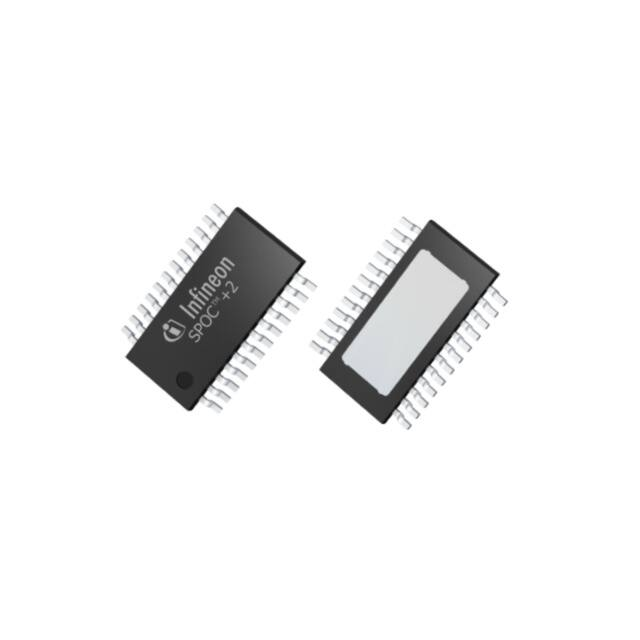


 工商网监
湘ICP备2023018690号
工商网监
湘ICP备2023018690号
