IFX25401
Low Dropout Linear Voltage Regulator
IFX25401TBV
IFX25401TEV
IFX25401TBV50
IFX25401TEV50
Data Sheet
Rev. 1.02, 2012-08-24
Standard Power
�Low Dropout Linear Voltage Regulator
IFX25401
Features
•
•
•
•
•
•
•
•
•
•
Output Voltage Versions: 5V and Adjustable
Very Low Current Consumption
400 mA Output Current Capability
Enable Input
Very Low Dropout Voltage
Output Current Limitation
Overtemperature Shutdown
Reverse Polarity Protection
Wide Temperature Range; -40 °C to 125 °C
Green Product (RoHS compliant)
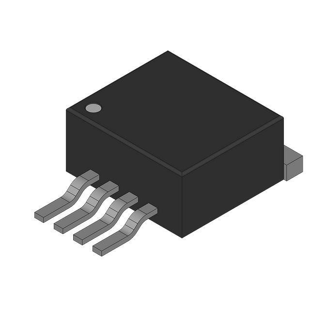
PG-TO263-5
Applications
•
•
•
•
•
Manufacturing and Automation
Medical Equipment
Building Management
Industrial White Goods
Security Systems
IFX25401 is not qualified and manufactured according to the
requirements of Infineon Technologies with regards to automotive and/or
transportation applications. For automotive applications please refer to
the Infineon TLx (TLE, TLS, TLF.....) voltage regulator products.
PG-TO252-5
Description
The IFX25401 is a monolithic integrated low dropout voltage regulator for load currents up to 400 mA. An input
voltage up to 40 V is regulated to an adjustable voltage with a precision of ±2%. The device is designed for harsh
environments. Therefore it is protected against overload, short circuit and overtemperature conditions by the
implemented output current limitation and the overtemperature shutdown circuit. The adustable output can be
configured to regulate between 2.5 V and 20 V.
Due to its very low quiescent current the IFX25401 is dedicated for use in applications permanently connected to
a battery. In addition the device can be switched off via the Enable input which reduces the current consumption
to less than 10 μA.
Type
Package
Marking
IFX25401TBV
PG-TO263-5
25401V
IFX25401TEV
PG-TO252-5
25401V
IFX25401TBV50
PG-TO263-5
25401V50
IFX25401TEV50
PG-TO252-5
2540150
Data Sheet
2
Rev. 1.02, 2012-08-24
�IFX25401
Block Diagram
1
Block Diagram
Saturation
Control and
Protection
Circuit
Temperature
Sensor
Ι
1
5
Control
Amplifier
Q
Buffer
Bandgap
Reference
*)
**)
2
4
3
EN
VA
GND
*) For fixed Voltage Regulator only
**) For adjustable Voltage Regulator only
Figure 1
Data Sheet
AEB02044
Block Diagram
3
Rev. 1.02, 2012-08-24
�IFX25401
Pin Configuration
2
Pin Configuration
2.1
Pin Assignment PG-TO263-5, PG-TO252-5
GND
GND
1
5
I
1 2 3 4 5
Q
EN n.c.
VA
I GND Q
EN n.c.
VA
AEP02560
PinConfig_PG-TO-263-5-1.vsd
Figure 2
Pin Configuration (top view)
2.2
Pin Definitions and Functions PG-TO263-5, PG-TO252-5
Pin No.
Symbol Function
1
I
Input
block to ground directly at the IC with a ceramic capacitor
2
EN
Enable
high level input signal enables the IC;
low level input signal disables the IC;
integrated pull-down resistor
3
GND
Ground
internally connected to heat slug
4
N.C.
Not Connected for IFX25401TBV50, IFX25401TEV50
can be open or connected to GND
Voltage Adjust for IFX25401TBV, IFX25401TEV
connect external voltage divider to configure the output voltage
VA
5
Q
Output
Connect a capacitor between Q and GND close to the IC pins and respect the values
specified for apacitance and ESR in “Functional Range” on Page 6
Heat Slug
–
Heat Slug
internally connected to GND;
connect to PCB/System GND and heatsink area
Data Sheet
4
Rev. 1.02, 2012-08-24
�IFX25401
General Product Characteristics
3
General Product Characteristics
3.1
Absolute Maximum Ratings
Absolute Maximum Ratings1)
Tj = -40 °C to 150 °C; all voltages with respect to ground, (unless otherwise specified)
Pos.
Parameter
Symbol
Limit Values
Unit
Test Condition
Min.
Max.
VI
-42
45
V
–
VEN
-42
45
V
–
Voltage
VVA
-0.3
10
V
–
Voltage
VQ
-1
40
V
–
Tj
Tstg
-40
150
°C
–
-50
150
°C
–
VESD,HBM
-2
2
kV
Human Body Model
(HBM)2)
VESD,CDM
-500
500
V
Charge Device
Model (CDM)3)
-750
750
V
Charge Device
Model (CDM) at
corner pins3)
Input I
3.1.1
Voltage
Enable EN
3.1.2
Voltage
Voltage Adjust Input VA
3.1.3
Output Q
3.1.4
Temperature
3.1.5
Junction temperature
3.1.6
Storage temperature
ESD Susceptibility
3.1.7
ESD Absorption
3.1.8
3.1.9
1) not subject to production test, specified by design
2) ESD susceptibility Human Body Model “HBM” according to JESD22-A114
3) ESD susceptibility Charged Device Model “CDM” according to ESDA STM5.3.1
Note: Stresses above the ones listed here may cause permanent damage to the device. Exposure to absolute
maximum rating conditions for extended periods may affect device reliability.
Note: Integrated protection functions are designed to prevent IC destruction under fault conditions described in the
data sheet. Fault conditions are considered as “outside” normal operating range. Protection functions are
not designed for continuous repetitive operation.
Data Sheet
5
Rev. 1.02, 2012-08-24
�IFX25401
General Product Characteristics
3.2
Pos.
3.2.10
Functional Range
Parameter
Input voltage
Symbol
VI
Limit Values
Unit
Remarks
IFX25401TBV, IFX25401TEV;
IFX25401TBV50, IFX25401TEV50
VQ > 4 V
Min.
Max.
VQ +
40
V
40
V
0.5
3.2.11
3.2.12
Input voltage
3.2.13
Output Capacitor’s
Requirements for Stability
3.2.14
Junction temperature
VI
4.5
IFX25401TBV, IFX25401TEV;
VQ < 4 V
CQ
22
ESR(CQ) –
Tj
-40
–
µF
1)
3
Ω
2)
125
°C
–
1) the minimum output capacitance requirement is applicable for a worst case capacitance tolerance of 30%
2) relevant ESR value at f = 10 kHz
Note: Within the functional or operating range, the IC operates as described in the circuit description. The electrical
characteristics are specified within the conditions given in the Electrical Characteristics table.
3.3
Thermal Resistance
Note: This thermal data was generated in accordance with JEDEC JESD51 standards. For more information, go
to www.jedec.org.
Pos.
Parameter
Symbol
Limit Values
Min.
Typ.
Max.
Unit
Conditions
IFX25401TBV, IFX25401TBV50 (PG-TO263-5)
3.3.1
Junction to Case1)
RthJC
–
4
–
K/W
measured to heat
slug
3.3.2
Junction to Ambient1)
RthJA
–
22
–
K/W
2)
3.3.3
–
74
–
K/W
footprint only3)
3.3.4
–
42
–
K/W
300 mm² heatsink
area3)
3.3.5
–
34
–
K/W
600 mm² heatsink
area3)
IFX25401TEV, IFX25401TEV50 (PG-TO252-5)
3.3.6
Junction to Case1)
RthJC
–
4
–
K/W
measured to heat
slug
3.3.7
Junction to Ambient1)
RthJA
–
27
–
K/W
2)
3.3.8
–
115
–
K/W
footprint only3)
3.3.9
–
52
–
K/W
300 mm² heatsink
area3)
3.3.10
–
40
–
K/W
600 mm² heatsink
area3)
1) Not subject to production test, specified by design.
2) Specified RthJA value is according to Jedec JESD51-2,-5,-7 at natural convection on FR4 2s2p board; The Product
(Chip+Package) was simulated on a 76.2 x 114.3 x 1.5 mm³ board with 2 inner copper layers (2 x 70µm Cu, 2 x 35µm Cu).
Where applicable a thermal via array under the exposed pad contacted the first inner copper layer.
Data Sheet
6
Rev. 1.02, 2012-08-24
�IFX25401
General Product Characteristics
3) Specified RthJA value is according to Jedec JESD 51-3 at natural convection on FR4 1s0p board; The Product
(Chip+Package) was simulated on a 76.2 × 114.3 × 1.5 mm3 board with 1 copper layer (1 x 70µm Cu).
Data Sheet
7
Rev. 1.02, 2012-08-24
�IFX25401
Electrical Characteristics
4
Electrical Characteristics
4.1
Electrical Characteristics Voltage Regulator
Electrical Characteristics
VI =13.5 V; Tj = -40 °C to 125 °C; all voltages with respect to ground (unless otherwise specified)
Pos.
Parameter
Symbol
Limit Values
Min.
Typ.
Max.
Unit
Measuring Condition
Output Q
4.1.1
Output Voltage Accuracy1)
ΔV Q
-2
–
2
%
IFX25401TBV,
IFX25401TEV
R2 < 50 kΩ;
VQ + 1 V ≤ VI ≤ 40V;
VI > 4.5 V;
5 mA ≤ IQ ≤ 400 mA
4.1.2
Output Voltage
VQ
4.9
5.0
5.1
V
IFX25401TBV50
IFX25401TEV50
6 V ≤ VI ≤ 28 V;
5 mA ≤ IQ ≤ 400 mA
4.1.3
Output Voltage Adjustable Range3) VQ,range
2.5
–
20
V
IFX25401TBV,
IFX25401TEV;
Refer to Page 13
4.1.4
Dropout Voltage
Vdr
–
250
500
mV
IQ = 250 mA
VI > 4.5 V;
Vdr = VI – VQ2)
4.1.5
Load Regulation
ΔVQ, lo
–
5
35
mV
IQ = 5 mA to 400 mA
VI = 4.5 V
4.1.6
Line Regulation
ΔVQ, li
–
15
25
mV
Vl = 12 V to 32 V
IQ = 5 mA
4.1.7
Output Current Limitation
IQ
400
600
1100
mA
2)
PSRR
dV Q
----------dT
–
54
–
dB
fr = 100 Hz; Vr = 0.5 Vpp
–
0.5
–
mV/K
–
4.1.8
4.1.9
Power Supply Ripple Rejection
3)
Temperature Output Voltage Drift
Data Sheet
3)
8
Rev. 1.02, 2012-08-24
�IFX25401
Electrical Characteristics
Electrical Characteristics
VI =13.5 V; Tj = -40 °C to 125 °C; all voltages with respect to ground (unless otherwise specified)
Pos.
Parameter
Symbol
Limit Values
Min.
Typ.
Max.
–
10
Unit
Measuring Condition
μA
VEN = 0 V
Current Consumption
Current Consumption,
Regulator Disabled
Iq
–
4.1.11
Quiescent Current
Iq = II – IQ
Iq
–
100
220
μA
IQ = 1 mA; VEN = 5 V
4.1.12
Current Consumption
Iq = II – IQ
Iq
–
5
10
mA
IQ = 250 mA; VEN = 5 V
4.1.13
Current Consumption
Iq = II – IQ
Iq
–
15
25
mA
IQ = 400 mA; VEN = 5 V
4.1.10
Tj ≤ 100 °C
1) influence of resistor divider on accuracy neglected
2) Measured when the output voltage VQ has dropped 100 mV from the nominal value obtained at VI = 13.5 V.
3) not subject to production test, specified by design
Data Sheet
9
Rev. 1.02, 2012-08-24
�IFX25401
Electrical Characteristics
4.2
Typical Performance Characteristics Voltage Regulator
Current Consumption Iq versus
Output Current IQ
Current Consumption Iq versus
Low Output Current IQ
16
02_IQ_IQLOW.VSD
1,4
01_IQ_IQ.VSD
14
1,2
V I = 13.5 V
T j = 25 °C
12
V I = 13.5 V
T j = 25 °C
1
I q [mA]
I q [mA]
10
8
6
0,8
0,6
0,4
4
2
0,2
0
0
0
100
200
300
0
400
20
Output Voltage VQ versus
Junction Temperature TJ
03_VQ_TJ.VSD
0,4
0,3
T j = 25 °C
400
0,2
350
0,1
300
0
-0,1
200
150
-0,3
100
-0,4
50
-0,5
80
120
T j = -40 °C
250
-0,2
40
T j = 150 °C
450
V DR [mV]
ΔV Q [%]
100
04_VDR_IQ.VSD
500
I Q = 5 mA
V I = 13.5 V
0
150
0
T j [°C]
Data Sheet
80
Dropout Voltage Vdr versus
Output Current IQ
0,5
0
60
I Q [mA]
I Q [mA]
-40
40
100
200
300
400
I Q [mA]
10
Rev. 1.02, 2012-08-24
�IFX25401
Electrical Characteristics
Dropout Voltage Vdr versus
Junction Temperature
Maximum Output Current IQ versus
Input Voltage VI
05_VDR_TJ.VSD
500
450
800
400
I Q = 400 mA
350
300
I Q,max [mA]
V DR [mV]
06_IQMAX_VI.VSD
900
250
200
I Q = 100 mA
150
700
T j = 25 °C
600
T j = -40 °C
T j = 150 °C
500
400
300
100
200
V Q = V Q,nom - 100 mV
I Q = 10 mA
50
100
0
-40
0
40
80
120
0
160
0
T j [°C]
10
20
30
40
V I [V]
Region Of Stability: Output Capacitor’s ESR
ESR(CQ) versus Output Current IQ
ESR(C Q ) [Ω ]
10
07_ESR_IQ.VSD
Unstable
Region
1
C Q = 22 µF
V I = 13.5 V
Stable
Region
0,1
0,01
0
100
200
300
400
I Q [mA]
Data Sheet
11
Rev. 1.02, 2012-08-24
�IFX25401
Electrical Characteristics
4.3
Electrical Characteristics Enable Function
The Enable Function allows disabling/enabling the regulator via the input pin EN. The regulator is turned on in
case the pin EN is connected to a voltage higher than VEN,H. This can be e.g. the battery voltage, whereby no
additional pull-up resistor is needed. The regulator can be turned off by connecting the pin EN to a voltage less
than VEN,L, e.g. GND.
Electrical Characteristics Enable
VI =13.5 V; Tj = -40 °C to 125 °C; all voltages with respect to ground, positive current flowing into pin
(unless otherwise specified)
Pos.
4.3.14
Parameter
Symbol
VEN,H
VEN,L
IEN,H
High Level Input Voltage
4.3.15
Low Level Input Voltage
4.3.16
High Level Input Current
4.4
Limit Values
Unit
Measuring Condition
V
VQ ≥ 4.9 V
VQ ≤ 0.1 V
VEN = 5 V
Min.
Typ.
Max.
3.5
–
–
–
–
0.5
V
5
10
20
µA
Typical Performance Characteristics Enable Function
Enabled Input Current IEN versus
Input Voltage VI , (Device OFF)
Enabled Input Current IEN versus
Enabled Input Voltage VEN (Device ON)
600
10_IEN_VEN.VSD
80
09_IEN_VI.VSD
V EN = 0.5 V
70
500
T j = 150 °C
60
400
I EN [µA]
I EN [nA]
50
300
V EN = 0.3 V
40
T j = 150 °C
T j = 25 °C
30
200
T j = -40 °C
20
100
10
V EN = 0.1 V
0
0
0
10
20
30
40
0
V I [V]
Data Sheet
10
20
30
40
V EN [V]
12
Rev. 1.02, 2012-08-24
�IFX25401
Application Information
5
Application Information
Note: The following information is given as a hint for the implementation of the device only and shall not be
regarded as a description or warranty of a certain functionality, condition or quality of the device.
I 1
Input
CI
2
4
3
GND
*) Optional
Figure 3
CQ
IFX25401
EN
e.g. KL 15
Output
5 Q
R 1*)
*)
VA
Voltage
Adjust
R 2*)
for adjustable Voltage Regulator
Application Diagram
A typical application circuit of the IFX25401 is shown in Figure 3. It shows a generic configuration of the voltage
regulator with a recommended minimum number of components. The small input capacitor is not required but
recommended for high frequency noise filtering. For a normal operation the fixed output voltage regulator only
requires an output capacitor for stability. The adjustable output regulator requires an additional resistor network to
configure the output voltage. Depending on the application conditons, additional components such as an input
buffer capacitor or a reverse polarity protection diode can be considered as well.
Input Filter Capacitor
A small ceramic capacitor (e.g. 100nF in Figure 3) at the device’s input helps filtering high frequency noise. To
reach the best filter effect, this capacitor should be placed as close as possible to the device’s input pin. The input
filter capacitor does not have an influence on the stability of the device’s regulation loop.
Output Capacitor CQ
The output capacitor is the only external component that is required because it is part of the regulation loop. To
maintain stability of this regulation loop, the IFX25401 requires an output capacitor respecting the values given in
“Functional Range” on Page 6.
Adjusting the Output Voltage of Variable Output Regulators IFX25401TBV, IFX25401TEV
The output voltage of the IFX25401TBV and the IFX25401TEV can be adjusted between 2.5 V and 20 V by an
external resistor divider connected to the voltage adjust pin VA.
The VA pin is connected to the internal error amplifier comparing the voltage at this pin with the internal reference
voltage (i.e. 2.5 V).
Data Sheet
13
Rev. 1.02, 2012-08-24
�IFX25401
Application Information
5 Q
Internal
Reference
2.5 V Typical
Current
and
Saturation
Control
Vref
CQ
R1
22 µF
4 VA
R2
AEB02804
Figure 4
External Components at Output for Variable Voltage Regulator
The output voltage can be easily calculated, neglecting the current flowing into the VA pin:
R1 + R2
V Q = ------------------- × V ref
R2
where
R 2 < 50 kΩ
to neglect the current flowing into the VA pin,
with:
•
•
•
Vref: internal reference voltage, typically 2.5V
R1: resistor between regulator output Q and voltage adjust pin VA
R2: resistor between voltage adjust pin VA and GND
For a 2.5 V output voltage the output pin Q has to be directly connected to the adjust pin VA.
Take into consideration, that the accuracy of the resistors R1 and R2 adds an additional error to the output voltage
tolerance.
Data Sheet
14
Rev. 1.02, 2012-08-24
�IFX25401
Package Outlines
6
Package Outlines
4.4
10 ±0.2
1.27 ±0.1
A
8.5 1)
B
0.05
2.4
0.1
2.7 ±0.3
4.7 ±0.5
7.55 1)
9.25 ±0.2
(15)
1±0.3
0...0.3
0...0.15
5 x 0.8 ±0.1
0.5 ±0.1
4 x 1.7
0.25
M
A B
8˚ MAX.
1) Typical
Metal surface min. X = 7.25, Y = 6.9
All metal surfaces tin plated, except area of cut.
Figure 5
Data Sheet
0.1 B
GPT09113
PG-TO263-5
15
Rev. 1.02, 2012-08-24
�IFX25401
Package Outlines
6.5 +0.15
-0.05
A
1)
2.3 +0.05
-0.10
0.9 +0.20
-0.01
0...0.15
5 x 0.6 ±0.1
1.14
4.56
0.5 +0.08
-0.04
0.51 MIN.
0.15 MAX.
per side
B
(5)
0.8 ±0.15
(4.24) 1 ±0.1
9.98 ±0.5
6.22 -0.2
5.7 MAX.
0.5 +0.08
-0.04
0.1 B
0.25 M A B
1) Includes mold flashes on each side.
All metal surfaces tin plated, except area of cut.
Figure 6
PG-TO252-5
Green Product (RoHS compliant)
To meet the world-wide customer requirements for environmentally friendly products and to be compliant with
government regulations the device is available as a green product. Green products are RoHS-Compliant (i.e
Pb-free finish on leads and suitable for Pb-free soldering according to IPC/JEDEC J-STD-020).
For further information on packages, please visit our website:
http://www.infineon.com/packages.
Data Sheet
16
Dimensions in mm
Rev. 1.02, 2012-08-24
�IFX25401
Revision History
7
Revision History
Revision
Date
Changes
1.02
2012-08-24
Coverpage changed, Additional information about the ENABLE pin added,
Disclaimer Updated
1.01
2009-10-19
Coverpage changed
Overview page: Inserted reference statement to TLE/TLF series.
1.0
2009-04-28
Initial Release
Data Sheet
17
Rev. 1.02, 2012-08-24
�Edition 2012-08-24
Published by
Infineon Technologies AG
81726 Munich, Germany
© 2012 Infineon Technologies AG
All Rights Reserved.
Legal Disclaimer
The information given in this document shall in no event be regarded as a guarantee of conditions or
characteristics. With respect to any examples or hints given herein, any typical values stated herein and/or any
information regarding the application of the device, Infineon Technologies hereby disclaims any and all warranties
and liabilities of any kind, including without limitation, warranties of non-infringement of intellectual property rights
of any third party.
Information
For further information on technology, delivery terms and conditions and prices, please contact the nearest
Infineon Technologies Office (www.infineon.com).
Warnings
Due to technical requirements, components may contain dangerous substances. For information on the types in
question, please contact the nearest Infineon Technologies Office.
The Infineon Technologies component described in this Data Sheet may be used in life-support devices or
systems and/or automotive, aviation and aerospace applications or systems only with the express written approval
of Infineon Technologies, if a failure of such components can reasonably be expected to cause the failure of that
life-support automotive, aviation and aerospace device or system or to affect the safety or effectiveness of that
device or system. Life support devices or systems are intended to be implanted in the human body or to support
and/or maintain and sustain and/or protect human life. If they fail, it is reasonable to assume that the health of the
user or other persons may be endangered.
�


 工商网监
湘ICP备2023018690号
工商网监
湘ICP备2023018690号
