31 May, 2011
IRS21867S
HIGH AND LOW SIDE DRIVER
Product Summary
Features
•
•
•
•
•
•
•
•
•
•
•
•
Floating channel designed for bootstrap operation
Fully operational to +600V
Tolerant to negative transient voltage, dV/dt
immune
Low VCC operation
Gate drive supply range from 5V to 20V
Undervoltage lockout for both channels
3.3V and 5V input logic compatible
Matched propagation delay for both channels
Logic and power ground +/- 5V offset
Lower di/dt gate driver for better noise immunity
Output source/sink current capability 4.0A (Typ.)
Leadfree, RoHS compliant
Topology
Single-Phase
VOFFSET
≤ 600V
VOUT
10V – 20V
Io+ & I o- (typical)
4.0A & 4.0A
ton & toff (typical)
170ns & 170ns
Package Options
Applications
• Battery powered equipment
• Hand-tools
• Fork-lifts
• Golf-carts
• RC Hobby Equipment
• E-bike
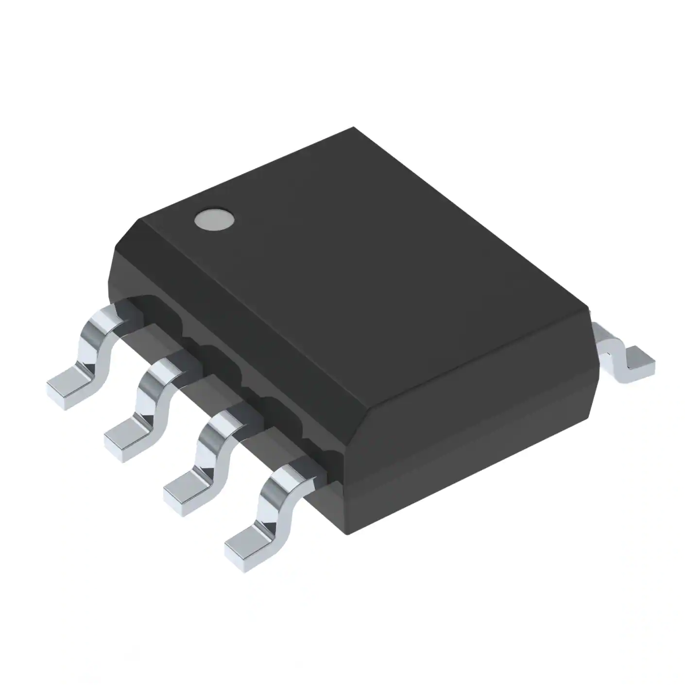
SOIC-8
Typical Connection Diagram
IRS21867S
Refer to Lead Assignment for correct pin
Configuration. This diagrams show electrical
Connections only. Please refer to our Application
Notes and Design Tips for proper circuit board layout
www.irf.com
© 2008 International Rectifier
�IRS21867S
Table of Contents
Page
Typical Connection Diagram
1
Description/Feature Comparison
3
Qualification Information
3
Absolute Maximum Ratings
4
Recommended Operating Conditions
4
Dynamic Electrical Characteristics
5
Static Electrical Characteristics
5
Functional Block Diagram
6
Input/Output Pin Equivalent Circuit Diagram
7
Lead Definitions
8
Lead Assignments
8
Application Information and Additional Details
9
Package Details
17
Tape and Reel Details
18
Part Marking Information
19
Ordering Information
20
www.irf.com
© 2010 International Rectifier
2
�IRS21867S
Description
The IRS21867 is a high voltage, high speed power MOSFET and IGBT driver with independent high and low
side referenced output channels. Proprietary HVIC and latch immune CMOS technologies enable ruggedized
monolithic construction. Low VCC operation allows use in battery powered applications. The logic input is
compatible with standard CMOS or LSTTL output, down to 3.3 V logic. The output drivers feature a high
pulse current buffer stage designed for minimum driver cross-conduction. The floating channel can be used
to drive an N-channel power MOSFET or IGBT in the high-side configuration which operates up to 600V.
†
Qualification Information
††
Industrial
Comments: This family of ICs has passed JEDEC’s
Industrial qualification. IR’s Consumer qualification level is
granted by extension of the higher Industrial level.
Qualification Level
Moisture Sensitivity Level
SOIC8N
†††
MSL2 260°C
(per IPC/JEDEC J-STD-020)
Class A
(per JEDEC standard JESD22-A115)
Class 2
(per EIA/JEDEC standard EIA/JESD22-A114)
Class I, Level A
(per JESD78)
Yes
Machine Model
ESD
Human Body Model
IC Latch-Up Test
RoHS Compliant
†
††
Qualification standards can be found at International Rectifier’s web site http://www.irf.com/
Higher qualification ratings may be available should the user have such requirements. Please contact
your International Rectifier sales representative for further information.
††† Higher MSL ratings may be available for the specific package types listed here. Please contact your
International Rectifier sales representative for further information.
www.irf.com
© 2010 International Rectifier
3
�IRS21867S
Absolute Maximum Ratings
Absolute Maximum Ratings indicate sustained limits beyond which damage to the device may occur. All
voltage parameters are absolute voltages referenced to COM. The thermal resistance and power dissipation
ratings are measured under board mounted and still air conditions.
Symbol
VB
Definition
Min
Max
High side floating absolute voltage
-0.3
625 (Note 1)
VB – 25
VS - 0.3
-0.3
-0.3
COM - 0.3
—
—
—
—
-50
—
VB + 0.3
VB + 0.3
25 (Note 1)
VCC + 0.3
VCC + 0.3
50
0.625
200
150
150
300
VS
High side floating supply offset voltage
VHO
High side floating output voltage
VCC
Low side and logic fixed supply voltage
VLO
Low side output voltage
VIN
Logic input voltage (HIN & LIN)
dVS/dt
Allowable offset supply voltage transient
PD
Package power dissipation @ TA ≤ 25°C
RthJA
Thermal resistance, junction to ambient
TJ
Junction temperature
TS
Storage temperature
TL
Lead temperature (soldering, 10 seconds)
Note 1: All supplies are fully tested at 25V.
Units
V
V/ns
W
°C/W
°C
Recommended Operating Conditions
For proper operation the device should be used within the recommended conditions. All voltage parameters
are absolute voltages referenced to COM. The VS offset rating is tested with all supplies biased at (VCCCOM) = 15V.
Symbol
Definition
Min
Max
Units
VB
High side floating supply absolute voltage
VS + 10
VS + 20
VS
High side floating supply offset voltage
Note 2
600
VHO
High side floating output voltage
VS
VB
V
VCC
Low side and logic fixed supply voltage
10
20
VLO
Low side output voltage
0
VCC
VIN
Logic input voltage (HIN & LIN)
COM
VCC
TA
Ambient temperature
-40
125
°C
† Note 2: Logic operational for VS of -5V to +600V. Logic state held for VS of -5V to –VBS. (Please refer to
the Design Tip DT97-3 for more details).
www.irf.com
© 2010 International Rectifier
4
�IRS21867S
Dynamic Electrical Characteristics
VCC = VBS = 15V, CL = 1000 pF, TA = 25°C unless otherwise specified.
Symbol
ton
toff
MT
tr
tf
Min Typ Max Units Test Conditions
Definition
Turn-on propagation delay
Turn-off propagation delay
Delay matching | ton – toff |
Turn-on rise time
Turn-off fall time
—
—
—
—
—
170
170
—
22
18
250
250
35
38
30
ns
VS = 0V
VS = 0V or 600V
VS = 0V
Static Electrical Characteristics
VCC = VBS = 15V,, and TA = 25°C unless otherwise specified. The VIN, and IIN parameters are referenced to
COM and are applicable to the respective input leads: HIN, and LIN. The VO, and IO parameters are
referenced to VS/COM and are applicable to the respective output leads: HO and LO.
Symbol
VIH
VIL
VOH
VOL
ILK
IQBS
IQCC
IIN+
IINVCCUV+
VBSUV+
VCCUVVBSUVVCCUVH
VBSUVH
Definition
Logic “1” input voltage for HO & LO
Logic “0” input voltage for HO & LO
High level output voltage, VCC or VBS - VO
Low level output voltage, VO
Offset supply leakage current
Quiescent VBS supply current
Quiescent VCC supply current
Logic “1” input bias current
Logic “0” input bias current
VCC and VBS supply undervoltage positive
going threshold
VCC and VBS supply undervoltage negative
going threshold
Min
Typ Max Units Test Conditions
2.5
—
—
—
—
20
50
—
—
—
—
—
0.8
—
1.4
— 0.15
—
50
60 150
120 240
250 —
—
5.0
5.34
6
0.5
IO+
Output high short circuit pulsed current
4.0
IO-
Output low short circuit pulsed current
4.0
VIN = 0V or 5V
µA
HIN = LIN = 5V
HIN = LIN = 0V
V
A
www.irf.com
IO = 0mA
IO = 20mA
VB = VS = 600 V
6.66
4.90 5.50 6.10
VCC and VBS supply undervoltage Hysteresis
VCC = 10V to 20V
V
VO = 0V,
PW ≤ 10µs
VO = 15V,
PW ≤ 10µs
© 2010 International Rectifier
5
�IRS21867S
Functional Block Diagrams
IRS21867
www.irf.com
© 2010 International Rectifier
6
�IRS21867S
Input/Output Pin Equivalent Circuit Diagrams
VB
ESD
Diode
25V
HO
ESD
Diode
VS
600V
VCC
ESD
Diode
LO
25V
ESD
Diode
COM
COM/V
SS
COM
www.irf.com
© 2010 International Rectifier
7
�IRS21867S
Lead Definitions: IRS21867S
Pin#
1
2
3
4
5
6
7
8
Symbol
VCC
HIN
LIN
COM
LO
VS
HO
VB
Description
Low-side and logic fixed supply
Logic input for high-side gate driver output (HO), in phase with HO
Logic input for low-side gate driver output (LO), in phase with LO
Low-side return
Low-side gate drive output
High-side floating supply return
High-side gate drive output
High-side floating supply
Lead Assignments
8 lead SOIC
IRS21867S
www.irf.com
© 2010 International Rectifier
8
�IRS21867S
Application Information and Additional Details
Informations regarding the following topics are included as subsections within this section of the datasheet.
•
•
•
•
•
•
•
•
IGBT/MOSFET Gate Drive
Switching and Timing Relationships
Matched Propagation Delays
Input Logic Compatibility
Undervoltage Lockout Protection
Negative VS Transient SOA
PCB Layout Tips
Additional Documentation
IGBT/MOSFET Gate Drive
The IRS21867 HVIC is designed to drive MOSFET or IGBT power devices. Figures 1 and 2 illustrate several
parameters associated with the gate drive functionality of the HVIC. The output current of the HVIC, used to drive
the gate of the power switch, is defined as IO. The voltage that drives the gate of the external power switch is
defined as VHO for the high-side power switch and VLO for the low-side power switch; this parameter is sometimes
generically called VOUT and in this case does not differentiate between the high-side or low-side output voltage.
VB
(or VCC)
VB
(or VCC)
IO+
HO
(or LO)
HO
(or LO)
+
IO-
VHO (or VLO)
VS
(or COM)
-
VS
(or COM)
Figure 1: HVIC sourcing current
Figure 2: HVIC sinking current
www.irf.com
© 2010 International Rectifier
9
�IRS21867S
Switching and Timing Relationships
The relationships between the input and output signals of the IRS21867 are illustrated below in Figures 3, 4. From
these figures, we can see the definitions of several timing parameters (i.e., PW IN, PW OUT, tON, tOFF, tR, and tF)
associated with this device.
LINx
(or HINx)
50%
50%
PWIN
tON
LOx
(or HOx)
tOFF
tR
tF
PWOUT
90%
90%
10%
10%
Figure 3: Switching time waveforms
Figure 4: Input/output timing diagram
Matched Propagation Delays
The IRS21867 is designed with propagation delay matching circuitry. With this feature, the IC’s response at the
output to a signal at the input requires approximately the same time duration (i.e., tON, tOFF) for both the low-side
channels and the high-side channels; the maximum difference is specified by the delay matching parameter (MT).
The propagation turn-on delay (tON) is matched to the propagation turn-on delay (tOFF).
www.irf.com
© 2010 International Rectifier
10
�IRS21867S
Figure 5: Delay Matching Waveform Definition
Input Logic Compatibility
The inputs of this IC are compatible with standard CMOS and TTL outputs. The IRS21867 has been designed to be
compatible with 3.3 V and 5 V logic-level signals. Figure 8 illustrates an input signal to the IRS22867, its input
threshold values, and the logic state of the IC as a result of the input signal.
Input Signal
(IRS23364D)
V IH
Input Logic
Level
VIL
High
Low
Low
Figure 6: HIN & LIN input thresholds
www.irf.com
© 2010 International Rectifier
11
�IRS21867S
Undervoltage Lockout Protection
This IC provides undervoltage lockout protection on both the VCC (logic and low-side circuitry) power supply and the
VBS (high-side circuitry) power supply. Figure 7 is used to illustrate this concept; VCC (or VBS) is plotted over time and
as the waveform crosses the UVLO threshold (VCCUV+/- or VBSUV+/-) the undervoltage protection is enabled or disabled.
Upon power-up, should the VCC voltage fail to reach the VCCUV+ threshold, the IC will not turn-on. Additionally, if the
VCC voltage decreases below the VCCUV- threshold during operation, the undervoltage lockout circuitry will recognize a
fault condition and shutdown the high- and low-side gate drive outputs.
Upon power-up, should the VBS voltage fail to reach the VBSUV threshold, the IC will not turn-on. Additionally, if the
VBS voltage decreases below the VBSUV threshold during operation, the undervoltage lockout circuitry will recognize a
fault condition, and shutdown the high-side gate drive outputs of the IC.
The UVLO protection ensures that the IC drives the external power devices only when the gate supply voltage is
sufficient to fully enhance the power devices. Without this feature, the gates of the external power switch could be
driven with a low voltage, resulting in the power switch conducting current while the channel impedance is high; this
could result in very high conduction losses within the power device and could lead to power device failure.
Figure 7: UVLO protection
www.irf.com
© 2010 International Rectifier
12
�IRS21867S
Tolerant to Negative VS Transients
A common problem in today’s high-power switching converters is the transient response of the switch node’s voltage
as the power switches transition on and off quickly while carrying a large current. A typical 3-phase inverter circuit is
shown in Figure 8; here we define the power switches and diodes of the inverter.
If the high-side switch (e.g., the IGBT Q1 in Figures 9 and 10) switches off, while the U phase current is flowing to an
inductive load, a current commutation occurs from high-side switch (Q1) to the diode (D2) in parallel with the low-side
switch of the same inverter leg. At the same instance, the voltage node VS1, swings from the positive DC bus voltage
to the negative DC bus voltage.
Figure 8: Three phase inverter
DC+ BUS
Q1
ON
IU
VS1
Q2
OFF
D2
DC- BUS
Figure 9: Q1 conducting
Figure 10: D2 conducting
Also when the V phase current flows from the inductive load back to the inverter (see Figures 11 and 12), and Q4
IGBT switches on, the current commutation occurs from D3 to Q4. At the same instance, the voltage node, VS2,
swings from the positive DC bus voltage to the negative DC bus voltage.
www.irf.com
© 2010 International Rectifier
13
�IRS21867S
Figure 11: D3 conducting
Figure 12: Q4 conducting
However, in a real inverter circuit, the VS voltage swing does not stop at the level of the negative DC bus, rather it
swings below the level of the negative DC bus. This undershoot voltage is called “negative VS transient”.
The circuit shown in Figure 13 depicts one leg of the three phase inverter; Figures 14 and 15 show a simplified
illustration of the commutation of the current between Q1 and D2. The parasitic inductances in the power circuit from
the die bonding to the PCB tracks are lumped together in LC and LE for each IGBT. When the high-side switch is on,
VS1 is below the DC+ voltage by the voltage drops associated with the power switch and the parasitic elements of the
circuit. When the high-side power switch turns off, the load current momentarily flows in the low-side freewheeling
diode due to the inductive load connected to VS1 (the load is not shown in these figures). This current flows from the
DC- bus (which is connected to the COM pin of the HVIC) to the load and a negative voltage between VS1 and the
DC- Bus is induced (i.e., the COM pin of the HVIC is at a higher potential than the VS pin).
Figure 13: Parasitic Elements
Figure 14: VS positive
Figure 15: VS negative
In a typical motor drive system, dV/dt is typically designed to be in the range of 3-5 V/ns. The negative VS transient
voltage can exceed this range during some events such as short circuit and over-current shutdown, when di/dt is
greater than in normal operation.
International Rectifier’s HVICs have been designed for the robustness required in many of today’s demanding
applications. An indication of the IRS21867’s robustness can be seen in Figure 16, where there is represented the
IRS2607 Safe Operating Area at VBS=15V based on repetitive negative VS spikes. A negative VS transient voltage
falling in the grey area (outside SOA) may lead to IC permanent damage; viceversa unwanted functional anomalies
or permanent damage to the IC do not appear if negative Vs transients fall inside SOA.
www.irf.com
© 2010 International Rectifier
14
�IRS21867S
Figure 16: Negative VS transient SOA for IRS2607 @ VBS=15V
Even though the IRS21867 has been shown able to handle these large negative VS transient conditions, it is highly
recommended that the circuit designer always limit the negative VS transients as much as possible by careful PCB
layout and component use.
PCB Layout Tips
Distance between high and low voltage components: It’s strongly recommended to place the components tied to the
floating voltage pins (VB and VS) near the respective high voltage portions of the device. Please see the Case
Outline information in this datasheet for the details.
Ground Plane: In order to minimize noise coupling, the ground plane should not be placed under or near the
high voltage floating side.
Gate Drive Loops: Current loops behave like antennas and are able to receive and transmit EM noise (see
Figure 17). In order to reduce the EM coupling and improve the power switch turn on/off performance, the
gate drive loops must be reduced as much as possible. Moreover, current can be injected inside the gate
drive loop via the IGBT collector-to-gate parasitic capacitance. The parasitic auto-inductance of the gate
loop contributes to developing a voltage across the gate-emitter, thus increasing the possibility of a self
turn-on effect.
www.irf.com
© 2010 International Rectifier
15
�IRS21867S
Figure 17: Antenna Loops
Supply Capacitor: It is recommended to place a bypass capacitor (CIN) between the VCC and COM pins. A
ceramic 1 µF ceramic capacitor is suitable for most applications. This component should be placed as close
as possible to the pins in order to reduce parasitic elements.
Routing and Placement: Power stage PCB parasitic elements can contribute to large negative voltage
transients at the switch node; it is recommended to limit the phase voltage negative transients. In order to
avoid such conditions, it is recommended to 1) minimize the high-side emitter to low-side collector distance,
and 2) minimize the low-side emitter to negative bus rail stray inductance. However, where negative VS
spikes remain excessive, further steps may be taken to reduce the spike. This includes placing a resistor (5
Ω or less) between the VS pin and the switch node (see Figure 18), and in some cases using a clamping
diode between COM and VS (see Figure 19). See DT04-4 at www.irf.com for more detailed information.
Figure 18: VS resistor
Figure 19: VS clamping diode
Additional Documentation
Several technical documents related to the use of HVICs are available at www.irf.com; use the Site Search
function and the document number to quickly locate them. Below is a short list of some of these documents.
DT97-3: Managing Transients in Control IC Driven Power Stages
DT04-4: Using Monolithic High Voltage Gate Drivers
AN-978: HV Floating MOS-Gate Driver ICs
www.irf.com
© 2010 International Rectifier
16
�IRS21867S
Package Details: SOIC8N
www.irf.com
© 2010 International Rectifier
17
�IRS21867S
Tape and Reel Details: SOIC8N
LOADED TAPE FEED DIRECTION
A
B
H
D
F
C
NOTE : CONTROLLING
DIM ENSION IN M M
E
G
CARRIER TAPE DIMENSION FOR
Metric
Code
Min
Max
A
7.90
8.10
B
3.90
4.10
C
11.70
12.30
D
5.45
5.55
E
6.30
6.50
F
5.10
5.30
G
1.50
n/a
H
1.50
1.60
8SOICN
Imperial
Min
Max
0.311
0.318
0.153
0.161
0.46
0.484
0.214
0.218
0.248
0.255
0.200
0.208
0.059
n/a
0.059
0.062
F
D
C
B
A
E
G
H
REEL DIMENSIONS FOR 8SOICN
Metric
Code
Min
Max
A
329.60
330.25
B
20.95
21.45
C
12.80
13.20
D
1.95
2.45
E
98.00
102.00
F
n/a
18.40
G
14.50
17.10
H
12.40
14.40
www.irf.com
Imperial
Min
Max
12.976
13.001
0.824
0.844
0.503
0.519
0.767
0.096
3.858
4.015
n/a
0.724
0.570
0.673
0.488
0.566
© 2010 International Rectifier
18
�IRS21867S
Part Marking Information
www.irf.com
© 2010 International Rectifier
19
�IRS21867S
Ordering Information
P/n
IRS21867SPbF
IRS21867STRPbF
Package
SOIC8
SOIC8
Packing
Tube
Tape & Reel
www.irf.com
Pcs
95
2500
© 2010 International Rectifier
20
�IRS21867S
The information provided in this document is believed to be accurate and reliable. However, International Rectifier assumes no
responsibility for the consequences of the use of this information. International Rectifier assumes no responsibility for any
infringement of patents or of other rights of third parties which may result from the use of this information. No license is granted by
implication or otherwise under any patent or patent rights of International Rectifier. The specifications mentioned in this document are
subject to change without notice. This document supersedes and replaces all information previously supplied.
For technical support, please contact IR’s Technical Assistance Center
http://www.irf.com/technical-info/
WORLD HEADQUARTERS:
233 Kansas St., El Segundo, California 90245
Tel: (310) 252-7105
Revision History
Date
5/20/2010
6/10/2010
03/30/2011
05/27/2011
05/31/2011
Comment
Initial Draft
Changed ABS MAX to 25V,
Updated Iin+ to 250uA(Typ) to reflect 20kohm pull-down,
Removed Min spec (2A) from Io+/Io-,
Updated Block Diagram based on IRS2188 D/S
Add recommended operation condition note
Add ESD and Latch up specs
Add application info and ordering info
www.irf.com
© 2010 International Rectifier
21
�


 工商网监
湘ICP备2023018690号
工商网监
湘ICP备2023018690号
