TLE 8718 SA
Smart 18-Channel Lowside Switch with Micro Second Bus
Data Sheet
Rev. 1.1, 2012-07-31
Automotive Power
�TLE 8718 SA
Table of Contents
Table of Contents
1
1.1
Overview . . . . . . . . . . . . . . . . . . . . . . . . . . . . . . . . . . . . . . . . . . . . . . . . . . . . . . . . . . . . . . . . . . . . . . . 4
Device Description . . . . . . . . . . . . . . . . . . . . . . . . . . . . . . . . . . . . . . . . . . . . . . . . . . . . . . . . . . . . . . . . 5
2
Block Diagram . . . . . . . . . . . . . . . . . . . . . . . . . . . . . . . . . . . . . . . . . . . . . . . . . . . . . . . . . . . . . . . . . . . 7
3
3.1
3.2
3.3
Pin Configuration . . . . . . . . . . . . . . . . . . . . . . . . . . . . . . . . . . . . . . . . . . . . . . . . . . . . . . . . . . . . . . . . 8
Pin Assignment . . . . . . . . . . . . . . . . . . . . . . . . . . . . . . . . . . . . . . . . . . . . . . . . . . . . . . . . . . . . . . . . . . . 8
Pin Definitions and Functions . . . . . . . . . . . . . . . . . . . . . . . . . . . . . . . . . . . . . . . . . . . . . . . . . . . . . . . . 9
Abbreviations . . . . . . . . . . . . . . . . . . . . . . . . . . . . . . . . . . . . . . . . . . . . . . . . . . . . . . . . . . . . . . . . . . . 10
4
4.1
4.2
4.3
4.4
4.5
General Product Characteristics . . . . . . . . . . . . . . . . . . . . . . . . . . . . . . . . . . . . . . . . . . . . . . . . . . .
Test coverage (TC) in series production . . . . . . . . . . . . . . . . . . . . . . . . . . . . . . . . . . . . . . . . . . . . . . .
Absolute Maximum Ratings . . . . . . . . . . . . . . . . . . . . . . . . . . . . . . . . . . . . . . . . . . . . . . . . . . . . . . . .
Thermal Resistance . . . . . . . . . . . . . . . . . . . . . . . . . . . . . . . . . . . . . . . . . . . . . . . . . . . . . . . . . . . . . .
ESD . . . . . . . . . . . . . . . . . . . . . . . . . . . . . . . . . . . . . . . . . . . . . . . . . . . . . . . . . . . . . . . . . . . . . . . . . .
Operating Range . . . . . . . . . . . . . . . . . . . . . . . . . . . . . . . . . . . . . . . . . . . . . . . . . . . . . . . . . . . . . . . .
11
11
11
13
14
14
5
5.1
5.2
5.3
5.4
5.5
5.6
5.7
5.8
5.9
5.10
Power Stages . . . . . . . . . . . . . . . . . . . . . . . . . . . . . . . . . . . . . . . . . . . . . . . . . . . . . . . . . . . . . . . . . .
Functional Description . . . . . . . . . . . . . . . . . . . . . . . . . . . . . . . . . . . . . . . . . . . . . . . . . . . . . . . . . . . .
Power Stages OUT1 and OUT3 . . . . . . . . . . . . . . . . . . . . . . . . . . . . . . . . . . . . . . . . . . . . . . . . . . . . .
Power Stages OUT2 and OUT4 . . . . . . . . . . . . . . . . . . . . . . . . . . . . . . . . . . . . . . . . . . . . . . . . . . . . .
Power Stages OUT5...OUT8 . . . . . . . . . . . . . . . . . . . . . . . . . . . . . . . . . . . . . . . . . . . . . . . . . . . . . . .
Power Stages OUT9 and OUT10 . . . . . . . . . . . . . . . . . . . . . . . . . . . . . . . . . . . . . . . . . . . . . . . . . . . .
Power Stages OUT11...OUT14 . . . . . . . . . . . . . . . . . . . . . . . . . . . . . . . . . . . . . . . . . . . . . . . . . . . . .
Power Stages OUT15 and OUT16 . . . . . . . . . . . . . . . . . . . . . . . . . . . . . . . . . . . . . . . . . . . . . . . . . . .
Power Stages OUT17 and OUT18 . . . . . . . . . . . . . . . . . . . . . . . . . . . . . . . . . . . . . . . . . . . . . . . . . . .
Timing Diagram MSC to OUTn . . . . . . . . . . . . . . . . . . . . . . . . . . . . . . . . . . . . . . . . . . . . . . . . . . . . . .
Parallel connection of PS . . . . . . . . . . . . . . . . . . . . . . . . . . . . . . . . . . . . . . . . . . . . . . . . . . . . . . . . . .
15
15
15
17
19
21
23
26
28
30
30
6
6.1
6.2
6.3
6.4
Device Self Protection . . . . . . . . . . . . . . . . . . . . . . . . . . . . . . . . . . . . . . . . . . . . . . . . . . . . . . . . . . .
Short Circuit Protection . . . . . . . . . . . . . . . . . . . . . . . . . . . . . . . . . . . . . . . . . . . . . . . . . . . . . . . . . . . .
Over Temperature Shut Down . . . . . . . . . . . . . . . . . . . . . . . . . . . . . . . . . . . . . . . . . . . . . . . . . . . . . .
Battery Voltage Monitoring . . . . . . . . . . . . . . . . . . . . . . . . . . . . . . . . . . . . . . . . . . . . . . . . . . . . . . . . .
Electrical Characteristics . . . . . . . . . . . . . . . . . . . . . . . . . . . . . . . . . . . . . . . . . . . . . . . . . . . . . . . . . .
32
32
32
32
33
7
Supervisory (DIS5_10, DELAYIN, DELAYOUT) . . . . . . . . . . . . . . . . . . . . . . . . . . . . . . . . . . . . . . . 34
8
8.1
8.2
8.3
8.4
8.5
8.6
Diagnosis . . . . . . . . . . . . . . . . . . . . . . . . . . . . . . . . . . . . . . . . . . . . . . . . . . . . . . . . . . . . . . . . . . . . . .
Diagnostic Functions . . . . . . . . . . . . . . . . . . . . . . . . . . . . . . . . . . . . . . . . . . . . . . . . . . . . . . . . . . . . .
Encoding of Diagnostic Information . . . . . . . . . . . . . . . . . . . . . . . . . . . . . . . . . . . . . . . . . . . . . . . . . .
State Diagram of the Device Diagnosis . . . . . . . . . . . . . . . . . . . . . . . . . . . . . . . . . . . . . . . . . . . . . . .
Reset of the Diagnostic Information . . . . . . . . . . . . . . . . . . . . . . . . . . . . . . . . . . . . . . . . . . . . . . . . . .
Electrical Characteristics . . . . . . . . . . . . . . . . . . . . . . . . . . . . . . . . . . . . . . . . . . . . . . . . . . . . . . . . . .
Timing . . . . . . . . . . . . . . . . . . . . . . . . . . . . . . . . . . . . . . . . . . . . . . . . . . . . . . . . . . . . . . . . . . . . . . . . .
36
36
39
40
41
41
42
9
9.1
9.2
9.3
9.4
9.5
9.6
9.7
9.8
Supply, VDD Monitoring, Reset and ABE . . . . . . . . . . . . . . . . . . . . . . . . . . . . . . . . . . . . . . . . . . . .
General functions of VDD Monitoring . . . . . . . . . . . . . . . . . . . . . . . . . . . . . . . . . . . . . . . . . . . . . . . . . .
VDD Undervoltage . . . . . . . . . . . . . . . . . . . . . . . . . . . . . . . . . . . . . . . . . . . . . . . . . . . . . . . . . . . . . . . .
VDD Overvoltage . . . . . . . . . . . . . . . . . . . . . . . . . . . . . . . . . . . . . . . . . . . . . . . . . . . . . . . . . . . . . . . . .
Thresholds . . . . . . . . . . . . . . . . . . . . . . . . . . . . . . . . . . . . . . . . . . . . . . . . . . . . . . . . . . . . . . . . . . . . .
ABE Pin . . . . . . . . . . . . . . . . . . . . . . . . . . . . . . . . . . . . . . . . . . . . . . . . . . . . . . . . . . . . . . . . . . . . . . .
Testing of VDD Monitoring . . . . . . . . . . . . . . . . . . . . . . . . . . . . . . . . . . . . . . . . . . . . . . . . . . . . . . . . . .
Testing procedure of VDD Monitoring in the application . . . . . . . . . . . . . . . . . . . . . . . . . . . . . . . . . .
Electrical Characteristics . . . . . . . . . . . . . . . . . . . . . . . . . . . . . . . . . . . . . . . . . . . . . . . . . . . . . . . . . .
43
43
44
44
45
46
46
46
47
Data Sheet
2
Rev. 1.1, 2012-07-31
�TLE 8718 SA
Table of Contents
10
Device Logic Behavior . . . . . . . . . . . . . . . . . . . . . . . . . . . . . . . . . . . . . . . . . . . . . . . . . . . . . . . . . . . 50
11
11.1
11.1.1
11.1.2
11.1.3
11.1.4
11.2
11.3
11.4
11.5
Micro Second Channel MSC . . . . . . . . . . . . . . . . . . . . . . . . . . . . . . . . . . . . . . . . . . . . . . . . . . . . . .
Downstream Communication . . . . . . . . . . . . . . . . . . . . . . . . . . . . . . . . . . . . . . . . . . . . . . . . . . . . . . .
Voltage Level Diagrams of low voltage differential pins . . . . . . . . . . . . . . . . . . . . . . . . . . . . . . . . .
Downstream Supervisory Functions . . . . . . . . . . . . . . . . . . . . . . . . . . . . . . . . . . . . . . . . . . . . . . . .
Command Frame . . . . . . . . . . . . . . . . . . . . . . . . . . . . . . . . . . . . . . . . . . . . . . . . . . . . . . . . . . . . . . .
Data Frame . . . . . . . . . . . . . . . . . . . . . . . . . . . . . . . . . . . . . . . . . . . . . . . . . . . . . . . . . . . . . . . . . . .
Upstream Communication . . . . . . . . . . . . . . . . . . . . . . . . . . . . . . . . . . . . . . . . . . . . . . . . . . . . . . . . .
Timing Characteristics . . . . . . . . . . . . . . . . . . . . . . . . . . . . . . . . . . . . . . . . . . . . . . . . . . . . . . . . . . . .
Internal Clock Signal . . . . . . . . . . . . . . . . . . . . . . . . . . . . . . . . . . . . . . . . . . . . . . . . . . . . . . . . . . . . . .
Electrical Characteristics . . . . . . . . . . . . . . . . . . . . . . . . . . . . . . . . . . . . . . . . . . . . . . . . . . . . . . . . . .
52
53
54
54
54
55
57
58
58
59
12
Control of the device . . . . . . . . . . . . . . . . . . . . . . . . . . . . . . . . . . . . . . . . . . . . . . . . . . . . . . . . . . . .
12.1
Commands . . . . . . . . . . . . . . . . . . . . . . . . . . . . . . . . . . . . . . . . . . . . . . . . . . . . . . . . . . . . . . . . . . . . .
12.1.1
WR_OUT1516 . . . . . . . . . . . . . . . . . . . . . . . . . . . . . . . . . . . . . . . . . . . . . . . . . . . . . . . . . . . . . . . . .
12.1.2
WR_RST . . . . . . . . . . . . . . . . . . . . . . . . . . . . . . . . . . . . . . . . . . . . . . . . . . . . . . . . . . . . . . . . . . . . .
12.1.3
WR_START . . . . . . . . . . . . . . . . . . . . . . . . . . . . . . . . . . . . . . . . . . . . . . . . . . . . . . . . . . . . . . . . . . .
12.1.4
RD_CONFIG . . . . . . . . . . . . . . . . . . . . . . . . . . . . . . . . . . . . . . . . . . . . . . . . . . . . . . . . . . . . . . . . . .
12.1.5
RD_DATA . . . . . . . . . . . . . . . . . . . . . . . . . . . . . . . . . . . . . . . . . . . . . . . . . . . . . . . . . . . . . . . . . . . .
12.2
Registers . . . . . . . . . . . . . . . . . . . . . . . . . . . . . . . . . . . . . . . . . . . . . . . . . . . . . . . . . . . . . . . . . . . . . . .
12.2.1
CONREG1 . . . . . . . . . . . . . . . . . . . . . . . . . . . . . . . . . . . . . . . . . . . . . . . . . . . . . . . . . . . . . . . . . . . .
12.2.2
CONREG2 . . . . . . . . . . . . . . . . . . . . . . . . . . . . . . . . . . . . . . . . . . . . . . . . . . . . . . . . . . . . . . . . . . . .
12.2.3
CONREG3 . . . . . . . . . . . . . . . . . . . . . . . . . . . . . . . . . . . . . . . . . . . . . . . . . . . . . . . . . . . . . . . . . . . .
12.2.4
CONREG4 . . . . . . . . . . . . . . . . . . . . . . . . . . . . . . . . . . . . . . . . . . . . . . . . . . . . . . . . . . . . . . . . . . . .
12.2.5
OUT1516 . . . . . . . . . . . . . . . . . . . . . . . . . . . . . . . . . . . . . . . . . . . . . . . . . . . . . . . . . . . . . . . . . . . . .
12.2.6
OUTREG_EVEN . . . . . . . . . . . . . . . . . . . . . . . . . . . . . . . . . . . . . . . . . . . . . . . . . . . . . . . . . . . . . . .
12.2.7
OUTREG_ODD . . . . . . . . . . . . . . . . . . . . . . . . . . . . . . . . . . . . . . . . . . . . . . . . . . . . . . . . . . . . . . . .
12.2.8
DIAREG1 . . . . . . . . . . . . . . . . . . . . . . . . . . . . . . . . . . . . . . . . . . . . . . . . . . . . . . . . . . . . . . . . . . . . .
12.2.9
DIAREG2 . . . . . . . . . . . . . . . . . . . . . . . . . . . . . . . . . . . . . . . . . . . . . . . . . . . . . . . . . . . . . . . . . . . . .
12.2.10
DIAREG3 . . . . . . . . . . . . . . . . . . . . . . . . . . . . . . . . . . . . . . . . . . . . . . . . . . . . . . . . . . . . . . . . . . . . .
12.2.11
DIAREG4 . . . . . . . . . . . . . . . . . . . . . . . . . . . . . . . . . . . . . . . . . . . . . . . . . . . . . . . . . . . . . . . . . . . . .
12.2.12
DIAREG5 . . . . . . . . . . . . . . . . . . . . . . . . . . . . . . . . . . . . . . . . . . . . . . . . . . . . . . . . . . . . . . . . . . . . .
12.2.13
DIAREG6 . . . . . . . . . . . . . . . . . . . . . . . . . . . . . . . . . . . . . . . . . . . . . . . . . . . . . . . . . . . . . . . . . . . . .
12.2.14
DIAREG7 . . . . . . . . . . . . . . . . . . . . . . . . . . . . . . . . . . . . . . . . . . . . . . . . . . . . . . . . . . . . . . . . . . . . .
12.2.15
IDENTREG . . . . . . . . . . . . . . . . . . . . . . . . . . . . . . . . . . . . . . . . . . . . . . . . . . . . . . . . . . . . . . . . . . .
12.2.16
TESTREG . . . . . . . . . . . . . . . . . . . . . . . . . . . . . . . . . . . . . . . . . . . . . . . . . . . . . . . . . . . . . . . . . . . .
12.2.17
SEL_THRES . . . . . . . . . . . . . . . . . . . . . . . . . . . . . . . . . . . . . . . . . . . . . . . . . . . . . . . . . . . . . . . . . .
12.2.18
FUSE_SC . . . . . . . . . . . . . . . . . . . . . . . . . . . . . . . . . . . . . . . . . . . . . . . . . . . . . . . . . . . . . . . . . . . .
62
62
63
64
64
66
66
67
67
67
68
68
69
70
70
71
71
72
72
73
74
75
76
77
77
78
13
Application Information . . . . . . . . . . . . . . . . . . . . . . . . . . . . . . . . . . . . . . . . . . . . . . . . . . . . . . . . . . 79
14
Package Outlines . . . . . . . . . . . . . . . . . . . . . . . . . . . . . . . . . . . . . . . . . . . . . . . . . . . . . . . . . . . . . . . 80
15
Revision History . . . . . . . . . . . . . . . . . . . . . . . . . . . . . . . . . . . . . . . . . . . . . . . . . . . . . . . . . . . . . . . . 81
Data Sheet
3
Rev. 1.1, 2012-07-31
�Smart 18-Channel Lowside Switch with Micro Second Bus
speedFLEX
1
TLE8718SA
Overview
Features
•
•
•
•
•
•
•
•
•
•
•
•
•
Operating Conditions -40...150°C
Over Temperature Warning
ESD Capability 2/4KV HBM on-/off board Pins
Short Circuit Protected for VBAT = 36V
Active Zener Clamping at typically 55V
Open Load, Short to Ground, Short Circuit Diagnosis (2 bit/OUT)
Output control, diagnostics and initialisation via high speed
serial communication: Micro Second Channel [MSC]
all Pins protected against ≤36V
Over-Voltage and Under-Voltage Monitoring
Two Output Channels operating during low supply voltage possible
Programmable Short circuit behavior: switch off or current limitation
Green Product (RoHS compliant)
AEC Qualified
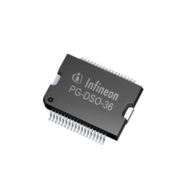
PG-DSO-36
Application
•
Automotive Engine Management Applications
•
Driver IC for inductive and ohmic actuators, such as Injectors, Solenoids, Relays, Lambda Heater.
Table 1
Output Stage Overview and Product Summary
Output
Maximum current
RON_max at Tj = 150°C without clamping
OUT1, OUT3
8A
200mΩ
OUT2, OUT4
3A
350mΩ
OUT5...OUT8
2.2A
720mΩ
OUT9...OUT10
2.2A
470mΩ
OUT11...OUT14
2.2A
720mΩ
OUT15, OUT16
0.6A
2400mΩ
OUT17, OUT18
0.6A
2400mΩ
Operating Voltage
VDD_RES
VDD_POR
VDD
VDS (AZ)
2.5V (defined behavior of the device)
Active Zener Voltage
3...3.5V (OUT15,16 delayed switch-off)
4.5...5.5V (operating range)
50...60V
Type
Package
Marking
TLE8718SA
PG-DSO-36
TLE8718SA
Data Sheet
4
Rev. 1.1, 2012-07-31
�TLE 8718 SA
Overview
1.1
Device Description
All stages are controlled by MSC interface. The MSC interface can be single ended or low voltage differential type.
Serial transmission of the error code (diagnostic) via MSC interface (upstream channel).
All power stages (PS) are protected against short circuit to battery voltage (SCB). All PS (OUT1...18) are equipped
with switch off mode and current control mode in case of SCB (configurable).
Diagnosis of open load (OL), short-circuit to ground (SCG), short-circuit to battery voltage (SCB) and over
temperature (DOT) individually for each PS.
The fault conditions SCB, SCG, OL and DOT are not stored until an integrated filtering time has expired. If, at one
output, several errors occur in a sequence, always the last detected error is stored (after filtering time). All fault
conditions are encoded in two bits per stage and stored in the corresponding MSC interface registers. Additionally
there is one common diagnostic bit for fault occurrence (FAILURE_FLAG) at any output and one common
diagnostic bit (COTW) for diagnosis over temperature (DOT). The diagnostic registers can be read via MSC
interface. During the start-bit of a read out cycle the corresponding diagnostic register is cleared, nevertheless the
status of the diagnostic register before the start-bit is send. Pull-down Diagnostic currents and Open Load OL can
be switched off by configuration for OUT11...18; (CONREG3 and OUT1516).
Each stage (OUT1...14, 17, 18) is controlled with a separate bit of the data frame (downstream channel). The
control bit is non inverting, i.e. if a control bit is ‘1’ the corresponding stage is off. Stages are disabled – i.e. switched
off and switching on disabled if VDD is too low (VDD undervoltage or power on reset) or VDD too high (VDD
overvoltage). The same applies when the MSC monitoring detects an error, micro controller reset is active (i.e.
external signal on pin RST = low or external signal on Pin ABE is logical low level).
All outputs are designed with internal zener diodes for applications with inductive loads.
OUT1 and OUT3 are designed for normal operation with 4A and extended current of 8A for maximum of 200
seconds each vehicle driving cycle.
OUT5...OUT10 are disabled by active low level on pins DIS5_10 (with short delay).
OUT9 and OUT10 are designed for actuators with higher clamping energy.
OUT15 and OUT16 can be forced OFF with the higher thresholds of DELAYIN (VDELAYIN_RES15_16_L and
VDELAYIN_RES15_16_H) (see Figure 8). OUT15 and OUT16 can be configured to delayed reset behavior, in this case,
the switching-off algorithm is delayed by internal filtering time (exception: power on reset (POR), RES15_16 and
valid command frame to switch off stages is not delayed).
Parallel connection of stages (OUT1...14, 17, 18) is possible as the control bits that switch on and off these stages
are all transmitted in the same data frame. OUT15 and OUT16 are only allowed to be connected to each other
and not to other stages (see Chapter 5.10).
DELAYOUT is pulled active low to switch off external components by the lower thresholds of DELAYIN (VDELAYIN_L
and VDELAYIN_H), ABE or VDD monitoring.
Data Sheet
5
Rev. 1.1, 2012-07-31
�TLE 8718 SA
Overview
tDIAG_OL
&
MUX
n=1…10
tDIAG_SCB
OFF/ON
RD_DATA
WR_RST
OL
n=1…4, 15…18
&
OUTn_SCB
SCB
S Flip
R Flop
≥1
tOUTn_OVSD
tOUTn_OVSON
SVBATT
RES15_16
STATUS_SVBATT
OUTn
tDELAYIN_GLITCH_x
Higher thresholds
of DELAYIN
DELAYIN_FIL
RES15_16_STATUS
≥1
R
≥1
S
Reset
„0"
V OUTn_B IAS
OUTn_DIA1/2
OUTn_DIA1/2
MUX
n=5...14
EXT_SCB
n=11...18
OUTn_DIAC
Reset
OUTn
Control
Flipflop
"Off"
&
&
"On, no delay "
OUTn_SCB OUTn_CONTROL
OUTn_DIAC OUTn_DELAY
"On, restart timeout "
≥1
&
&
"Keep State , restart
timeout“
tDELRES
Discard
≥1
&
Restart
n=15, 16
DIS5_10
tDIS5_10
DIS5_10_STATUS
n=5...10
TOUTn _OTSD
MSC downstream
D
OUTPUT_STBY
≥1
R
OUTn
Control
Flipflop
OUTREG
n=1...14, 17, 18
≥1
POR
tPOR
tRST
RST
MSC_MON
(timeout)
tMSC_MON
ABE_IMPACT
≥1
STAUS_UV
STATUS_OV
&
MUX
See „Block Diagramm V DD Monitoring“
ABE_STATUS
tFIL_OFF_DEL
READ_DIAREG6
VDD 28V. In that case, no function is available to be tested at VBAT = 40V).
4.2
Absolute Maximum Ratings
The integrated circuit will not be damaged if maximum ratings are reached. Every maximum rating is allowed to
be reached at the same time, as long as no other maximum rating is exceeded. But see Item Note:
Unless otherwise indicated all voltages are referred to PGND (all PGND and GNDABE are externally connected
to each other) Positive current flows into the pin.
Table 3
Maximum Ratings
Tj = -40°C to +150°C, all voltages with respect to PGND, positive current flowing into pin, unless otherwise
specified
Pos. Parameter
Symbol
Values
min.
max.
Unit TC Conditions
Supply and Power Pins
4.2.1 Supply Voltage Range
pin VDD, static
VDD_MR
-0.3
36
V
C
–
4.2.2 Battery Voltage
stages output pins via load
VBAT_MR
-1
40
V
C
–
4.2.3 Total current over the PGND
IPGND_MR
dVGND_MR
-38
38
A
C
–
-0.3
0.3
V
C
–
4.2.5 Output Stages
static voltage OUTn (n=1...18)
VOUTn_MR
-0.3
50
V
C
OUTn OFF
4.2.6 Short Circuit to VBAT
(single event)
VBAT_SC
-0.3
36
V
C
OUTn (n=1...18),
Figure 4
VSIP_MR, VSIN_MR,
-0.3
VSI_MR, VFCLP_MR,
VFCLN_MR, VFCL_MR,
VSSY_MR, VDIS5_10_MR,
VRST_MR
VABE_MR
-0.3
VDELAYOUT_MR,
-0.3
VSDO_MR
36
V
C
–
36
V
C
–
36
V
C
–
4.2.4 Ground Voltage Offset
maximum permissible offset
between GNDABE and the PGND
Interface and Logic
4.2.7 Logic Input Pins
SIP, SIN, SI,
FCLP, FCLN, FCL,
SSY, DIS5_10, RST
4.2.8 Bidirectional Pin ABE
4.2.9 Output Pins
DELAYOUT, SDO
Data Sheet
11
Rev. 1.1, 2012-07-31
�TLE 8718 SA
General Product Characteristics
Table 3
Maximum Ratings
Tj = -40°C to +150°C, all voltages with respect to PGND, positive current flowing into pin, unless otherwise
specified
Pos. Parameter
Symbol
Values
min.
4.2.10 Input Pins
DELAYIN, SVBATT
4.2.11 Current into Pin
SIP, SIN, SI,
FCLP, FCLN, FCL,
SSY, DIS5_10, RST,
DELAYIN, SVBATT, SDO
4.2.12 Current into Pin DELAYOUT, ABE
Unit TC Conditions
max.
VDELAYIN_MR,
-0.3
VSVBATT_MR
ISIP_MR, ISIN_MR, ISI_MR, -10
IFCLP_MR, IFCLN_MR,
IFCL_MR, ISSY_MR,
IDIS5_10_MR, IRST_MR,
IDELAYIN_MR,
ISVBATT_MR, ISDO_MR
IDELAYOUT_MR, IABE_MR -10
40
V
C
–
10
mA
C
1)
15
mA
C
1)
Tj
TSTG
-40
150
°C
C
–
-55
150
°C
C
–
Temperatures
4.2.13 Junction Temperature
4.2.14 Storage Temperature
1) Other maximum ratings (like Item 4.2.7 to Item 4.2.10 or Item 4.2.13) are not allowed to be exceeded.
Note: Stresses above the ones listed here may cause permanent damage to the device. Exposure to absolute
maximum rating conditions for extended periods may affect device reliability.
Note: Integrated protection functions are designed to prevent IC destruction under fault conditions described in the
data sheet. Fault conditions are considered as “outside” normal operating range. Protection functions are
not designed for continuous or repetitive operation.
5µH
80mΩ
0...5µH
10mΩ
LBAT
RHarness
LHarness
20mΩ
RECU
OUTn
RBAT
VBAT
PGND
Short_Circuit_test_setup.vsd
Figure 4
Data Sheet
Short Circuit test set-up
12
Rev. 1.1, 2012-07-31
�TLE 8718 SA
General Product Characteristics
4.3
Thermal Resistance
Note: This thermal data was generated in accordance with JEDEC JESD51 standards. For more information, go
to www.jedec.org.
Table 4
Thermal Resistance
Tj = -40°C to +150°C, all voltages with respect to PGND, positive current flowing into pin, unless otherwise
specified
Pos.
4.3.1
Parameter
Symbol
Junction to Case
Values
RthJC
RthJA
Unit TC Conditions
min.
typ.
max.
–
–
2
K/W C
1)
Junction to Ambient
–
25
–
K/W C see Figure 5 1)
1) Power dissipation Pv=3W distributed statically and homogeneously over all power stages. Resistive Load.
4.3.2
Dimensions : 76.2 x 114.3 x 1.6 mm³; Material: FR4
Thermal Vias: diameter = 0.3 mm; plating 25 µm; 56 pcs.
Metalization accodring : JEDEC 2s2p (JESD 51-7) + (JESD 51-5)
1.6 mm
70µm modeled (traces)
35µm, 90% metalization
35µm, 90% metalization
70µm, 5% metalization
Thermal_Setup .vsd
Figure 5
Data Sheet
Thermal simulation - PCB setup
13
Rev. 1.1, 2012-07-31
�TLE 8718 SA
General Product Characteristics
4.4
ESD
Of the various ESD models, the integrated circuit meets at least the “human body model” according to the
requirements of the EIA/JESD22-A114-F. During manufacturing process, ESD pulses according to "charged
device model" (EIA/JESD22-C101-D) may be exposed to each pin. ESD Specification Details in the following
Table.
Table 5
ESD Susceptibility
Tj = -40°C to +150°C, all voltages with respect to PGND, positive current flowing into pin, unless otherwise
specified
Pos.
Parameter
Symbol
Values
Unit TC Conditions
min.
typ.
max.
Standard Requirements for all Pins
4.4.1
Electro Static Discharge Voltage
“Human-Body-Model – HBM”
VESD1
-2
–
2
kV
C
All Pins
4.4.2
Electro Static Discharge Voltage
“Charged-Device-Model – CDM”
VESD2
-500
–
500
V
C
All Pins
Pins with Extended Requirements
4.4.3
Electro Static Discharge Voltage
“Human-Body-Model – HBM”
VESD3
-6
–
6
kV
C
OUT1…14
vs. PGND
4.4.4
Electro Static Discharge Voltage
“Human-Body-Model – HBM”
VESD4
-4
–
4
kV
C
OUT15…18
vs. PGND
4.5
Operating Range
Table 6
Operating Range
Tj = -40°C to +150°C, all voltages with respect to PGND, positive current flowing into pin, unless otherwise
specified
Pos.
Parameter
Symbol
Values
Unit TC
Conditions
V
C
–
13.5
V
C
–
0
A
C
1)
min.
max.
4.5
5.5
Supply, Battery Voltage
4.5.1
Supply Voltage Range
4.5.2
Battery Voltage
4.5.3
Nominal Total PGND Current
VDD
VBAT(typ)
IPGND(typ)
-12
1) Total PGND current influences e.g. the RON-measurement of the Power Stages or voltage thresholds of the input buffers
because of common PGND bond wires. As basis for definition of the RON or the voltage thresholds, the defined PGND
current is used.
Data Sheet
14
Rev. 1.1, 2012-07-31
�TLE 8718 SA
Power Stages
5
Power Stages
5.1
Functional Description
The following general description is valid for the channel groups OUT1,3, OUT2,4, OUT5...8, OUT9,10,
OUT11...14, OUT17,18. The specific function of the channel group OUT15,16 is described in Chapter 5.7.
The reset input of the OUTn-control flip-flop is active high and dominant, delivering a logic low level at the output
of the OUTn-control flip-flop.Only in failure-free condition, output can be switched on by MSC downstream.
Disabling inputs DIS5_10 and DELAYIN have different input characteristics and delay (tDELAYIN >> tDIS5_10). For
details concerning DIS5_10, DELAYIN and DELAYOUT see Chapter 7 and Figure 1.
5.2
Power Stages OUT1 and OUT3
Table 7
Electrical Characteristics Power Stages OUT1 and OUT3
n = 1 and 3, all channels ON or OFF, nominal load conditions, 4.5V < VDD < 5.5V, 4.5V < VBAT < 40V, all voltages
with respect to PGND, positive current flowing into pin. Tj = -40°C to +150°C, unless otherwise specified
Pos.
Parameter
Symbol
Values
Unit TC Conditions
min.
typ. max.
IOUTn
IOUTn_ex
tOUTn_ec
–
–
4
A
C
–
–
8
A
C
max 800h
–
–
60
h
C
VBAT≤14V,
RL≥0.88Ω
IOUTn_max
8
–
12.5
A
A
Ron-40_n
Ron+25_n
Ron+150_n
Ron_n
–
–
120
mΩ
C
–
–
148
mΩ
C
–
–
200
mΩ
A
–
–
210
mΩ
C
Ron-40_n
Ron+25_n
Ron+150_n
Ron_n
–
–
156
mΩ
C
–
–
193
mΩ
C
–
–
260
mΩ
A
–
–
273
mΩ
C
5.2.13 Switch on delay
tdon_n
–
–
15
µs
C
5.2.14 Switch off delay
tdoff_n
–
–
15
µs
C
5.2.15 Difference of switch on and off delay
tdif_n=tdon_n-tdoff_n
tdif_n
-8
–
8
µs
C
5.2.16 Switch on slew rates
son_n
0.5
1
2.5
V/µs C
Load Current
5.2.1
Continuous Load Current
5.2.2
Extended Load Current
5.2.3
Extended current time,
Accumulated operating time
5.2.4
Maximum current, (short circuit limited
current / switch off threshold)
ON-Resistance without clamping 1)
5.2.5
On Resistance Tj=-40°C
5.2.6
On Resistance Tj=25°C
5.2.7
On Resistance Tj=150°C
5.2.8
On Resistance Tj≤150°C
ON-Resistance with clamping
5.2.9
IOUTn=4A
IOUTn=4A
IOUTn=4A
IOUTn


 工商网监
湘ICP备2023018690号
工商网监
湘ICP备2023018690号
