SPX1117
800mA Low Dropout Voltage Regulator
September 2018
Rev. 2.1.1
GENERAL DESCRIPTION
APPLICATIONS
The SPX1117 is a low power positive-voltage
regulator designed to satisfy moderate power
requirements with a cost effective, small
footprint solution.
• Desktop PC Servers
This device is an excellent choice for use in
battery-powered applications and portable
computers. The SPX1117 features very low
quiescent current and a low dropout voltage of
1.1V at a full load. As output current
decreases, quiescent current flows into the
load, increasing efficiency. SPX1117 is
available in adjustable or fixed 1.5V, 1.8V,
2.5V, 3.3V and 5V output voltages.
• Power Supplies
• Graphic/Video Cards
• Industrial Equipments
FEATURES
• Guaranteed 800mA Output Current
• Guaranteed 1A Peak Current
• Three Terminal Adjustable or Fixed
1.5V, 1.8V, 2.5V, 3.3V and 5V
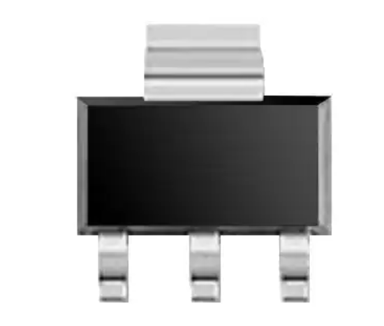
The SPX1117 is offered in a 3-pin SOT-223
surface mount packages.
• Low Quiescent Current
• Low Dropout Voltage of 1.1V at 800mA
An output capacitor of 10µF provides
unconditional stability while a smaller 2.2µF
capacitor is sufficient for most applications.
• 0.1% Line and 0.2% Load Regulation
• Stable with 2.2µF Ceramic Capacitor
• Overcurrent and Thermal Protection
• Lead Free, RoHS Compliant SOT223
Package
FUNCTIONAL DIAGRAM
Fig. 1: SPX1117 Application Diagram
1/11
Rev. 2.1.1
�SPX1117
800mA Low Dropout Voltage Regulator
ABSOLUTE MAXIMUM RATINGS
These are stress ratings only and functional operation of
the device at these ratings or any other above those
indicated in the operation sections of the specifications
below is not implied. Exposure to absolute maximum
rating conditions for extended periods of time may affect
reliability.
Power Dissipation ................................ Internally Limited
Lead Temperature (Soldering, 5 sec) ..................... 260°C
Storage Temperature .............................. -65°C to 150°C
Operating Junction Temperature Range ... -40°C to +125°C
Input Supply Voltage .............................................. 20V
Input to Output Voltage ........................................18.8V
ESD Rating (HBM - Human Body Model) .................... 2kV
ELECTRICAL SPECIFICATIONS
Specifications with standard type are for an Operating Ambient Temperature of TA = 25°C only; limits applying over the full
Operating Junction Temperature range are denoted by a “•”. Minimum and Maximum limits are guaranteed through test,
design, or statistical correlation. Typical values represent the most likely parametric norm at TJ = 25°C, and are provided for
reference purposes only. Unless otherwise indicated, CIN = COUT =10µF, TA= 25°C.
Parameter
Min.
Typ.
Max.
1.485
1.500
1.515
Units
Conditions
1.5V Version
Output Voltage
1.530
1.470
V
IOUT=5mA, VIN=3.0V, TJ=25°C
•
5mA≤ IOUT ≤800mA, 2.9V≤ VIN ≤10V
1.8V Version
Output Voltage
1.782
1.800
1.818
1.836
1.764
V
IOUT=5mA, VIN=3.3V, TJ=25°C
•
5mA≤ IOUT ≤800mA, 3.2V≤ VIN ≤10V
2.5V Version
Output Voltage
2.475
2.500
2.525
2.550
2.450
V
IOUT=5mA, VIN=4.0V, TJ=25°C
•
5mA≤ IOUT ≤800mA, 3.9V≤ VIN ≤10V
3.3V Version
Output Voltage
3.267
3.300
3.333
3.366
3.234
V
IOUT=5mA, VIN=4.8V, TJ=25°C
•
5.0V Version
Output Voltage
4.950
5.000
5.050
5.100
4.900
V
IOUT=5mA, VIN=6.5V, TJ=25°C
•
5mA≤ IOUT ≤800mA, 6.4V≤ VIN ≤12V
All Voltage Options
Reference Voltage
1.238
1.250
Output Voltage Temperature
Stability
1.262
1.270
1.225
0.3
V
3
7
mV
Load Regulation (note 1)
6
12
mV
1.00
1.20
1.05
1.25
1.10
1.30
Quiescent Current
5
10
Adjust Pin Current
50
120
1.5
2.0
A
0.01
0.1
%/W
Current Limit
1.0
Thermal Regulation
Ripple Rejection
60
5mA≤IOUT≤800mA, 1.4V≤(VIN–VOUT)≤10V
%
Line Regulation (note 1)
Dropout Voltage (note 2)
IOUT=5mA, (VIN – VOUT)=2V, TJ=25°C
•
75
•
5mA≤ IOUT ≤800mA, VOUT = Fixed/Adj.
•
IOUT=100mA
•
IOUT=500mA
•
IOUT=800mA
mA
•
4.25V≤ VIN ≤6.5V
µA
•
V
dB
2/11
VINMIN≤ VIN ≤12V, VOUT = Fixed/Adj.,
IOUT=5mA
(VIN – VOUT)=5V
25°C, 30ms pulse
fRIPPLE=120Hz, (VIN – VOUT)=2V,
VRIPPLE=1VPP
Rev. 2.1.1
�SPX1117
800mA Low Dropout Voltage Regulator
Parameter
Min.
Typ.
RMS Output Noise
Max.
Units
Conditions
0.03
%
125°C, 1000Hrs
0.003
%
% of VOUT, 10Hz≤f≤10kHz
Long Term Stability
Note 1:
For fixed voltage option VINMIN=VOUT+1.5V
For adjustable voltage option VIN-VOUT=1.4V
Note 2: Dropout voltage is the input voltage minus output voltage that produces a 1% decrease in output voltage with
respect to the nominal output voltage at VIN=VOUT+1.5V
PIN ASSIGNMENT
Fig. 2: SPX1117 Pin Assignment (Top View, TAB connected to VOUT)
ORDERING INFORMATION(1)
Part Number
Operating
Temperature Range
Lead-Free
Package
Packing Method
Output Voltage
Adjustable
SPX1117M3-L/TR
1.5V
SPX1117M3-L-1-5/TR
1.8V
SPX1117M3-L-1-8/TR
-40°C≤TJ≤+125°C
Yes(2)
SOT223-3
Tape & Reel
SPX1117M3-L-2-5/TR
2.5V
SPX1117M3-L-3-3/TR
3.3V
SPX1117M3-L-5-0/TR
5.0V
NOTE:
1.
Refer to www.exar.com/SPX1117 for most up-to-date Ordering Information.
2.
Visit www.exar.com for additional information on Environmental Rating.
3/11
Rev. 2.1.1
�SPX1117
800mA Low Dropout Voltage Regulator
TYPICAL PERFORMANCE CHARACTERISTICS
All data taken at TA = 25°C, unless otherwise specified - Schematic and BOM from Application Information section of this
datasheet.
Fig. 3: Load Regulation
SPX1117M3-L-3-3, VIN=4.8V
Fig. 4: Line Regulation
SPX1117M3-L-3-3, IOUT=10mA
Fig. 5: Dropout Voltage vs Output Current
SPX1117M3-L-3-3, VIN=4.8V, COUT=2.2µF
Fig. 6: Current Limit
IOUT pulsed from 10mA to Current limit
SPX1117M3-L-3-3, VIN=4.8V, CIN=COUT=2.2µF
Fig. 7: Current Limit
Output Voltage Deviation
SPX1117M3-L-3-3, IOUT=10mA to 1A Step
Fig. 8: VOUT vs Temperature
VIN=2.5V, IOUT=10mA
4/11
Rev. 2.1.1
�SPX1117
800mA Low Dropout Voltage Regulator
Fig. 9: VIN=3.0V, IOUT=10mA
Fig. 10: VIN=3.3V, IOUT=10mA
Fig. 11: VIN=4.0V, IOUT=10mA
Fig. 12: VIN=4.85V, IOUT=10mA
Fig. 13: Line Regulation vs Temperature
VOUT=1.8V (Adj), VIN=3.3V
Fig. 14: Output Voltage vs Temperature
Different IOUT, VOUT=1.8V (Adj), VIN=3.3V
Fig. 15: Line Regulation over Temperature
ILOAD=800mA, VOUT=1.8V(adj)
5/11
Rev. 2.1.1
�SPX1117
800mA Low Dropout Voltage Regulator
APPLICATION INFORMATION
OUTPUT CAPACITOR
To ensure the stability of the SPX1117, an
output capacitor of at least 2.2µF (tantalum or
ceramic) or 10µF (aluminum) is required. The
value may change based on the application
requirements
of
the
output
load
or
temperature range. The value of ESR can vary
based on the type of capacitor used in the
applications to guarantee stability. The
recommended value for ESR is 0.5Ω or less. A
larger value of output capacitance (up to
100µF) can improve the load transient
response.
Fig. 18
SOLDERING METHODS
The SPX1117 SOT-223 package is designed to
be compatible with infrared reflow or vaporphase reflow soldering techniques. During
soldering, the non-active or mildly active
fluxes may be used. The SPX1117 die is
attached to the heatsink lead which exits
opposite the input, output, and ground pins.
Hand soldering and wave soldering should be
avoided since these methods can cause
damage to the device with excessive thermal
gradients on the package. The SOT-223
recommended soldering method are as
follows: vapor phase reflow and infrared
reflow with the component preheated to within
65°C of the soldering temperature range.
Fig. 16: Load Step Response 0mA to 800mA
VIN=3.3V, VOUT=1.8V, CIN=10µF, COUT=2.2µF, Ceramic
Signal 1=VOUT, Signal 4=ILOAD
THERMAL CHARACTERISTICS
The thermal resistance of SPX1117 (SOT-223
package) is 15°C/W from junction to tab and
31°C/W from tab to ambient for a total of 46
°C/W from junction to ambient (Table 1). The
SPX1117 features the internal thermal limiting
to protect the device during overload
conditions. Special care needs to be taken
during continuous load conditions such that
the maximum junction temperature does not
exceed 125 °C. Thermal protection is activated
at >155°C and deactivated at


 工商网监
湘ICP备2023018690号
工商网监
湘ICP备2023018690号
