www.fairchildsemi.com
RC5532/RC5532A
High Performance Dual Low Noise Operational Amplifier
Features
• • • • • • • • Small signal bandwidth – 10 MHz Output drive capability – 600Ω, 10 VRMS Input noise voltage – 5 nV/ Hz DC voltage gain – 50,000 AC voltage gain – 2200 at 10 KHz Power bandwidth – 140 KHz Slew rate – 8 V/µS Large supply voltage range – ±3V to ±20V
Description
The RC5532 is a high performance, dual low noise operational amplifier. Compared to standard dual operational amplifiers, such as the RC747, it shows better noise performance, improved output drive capability, and considerably higher small-signal and power bandwidths. This makes the device especially suitable for application in high quality and professional audio equipment, instrumentation, control circuits, and telephone channel amplifiers. The op amp is internally compensated for gains equal to one. If very low noise is of prime importance, it is recommended that the RC5532A version be used which has guaranteed noise specifications.
Block Diagram
Output A –Input A +VS Output B
A
+Input A –VS
B
–Input B +Input B
65-5532-01
REV. 1.1.3 6/14/01
�RC5532/RC5532A
PRODUCT SPECIFICATION
Pin Assignments
8 PIN PDIP
Output (A) –Input (A) +Input (A) –VS 1 2 3 4 8 7 6 5 +VS Output (B) –Input (B) +Input (B)
Absolute Maximum Ratings
(beyond which the device may be damaged)1 Parameter Supply Voltage Input Voltage Differential Input Voltage PDTA < 50°C Junction Temperature Storage Temperature Operating Temperature Lead Soldering Temperature (10 sec) RC5532/A PDIP PDIP -65 0 Min. Typ. Max. ±22 ±VS 0.5 468 125 150 70 300 Units V V V mW °C °C °C °C
Notes: 1. Functional operation under any of these conditions is NOT implied. 2. For supply voltages less than ±15V, the absolute maximum input voltage is equal to the supply voltage. 3. Short circuit to ground on one amplifier only.
Operating Conditions
Parameter θJA Thermal resistance PDIP PDIP For TA > 50°C Derate at Min. Typ. 160 6.25 Max. Units °C/W mW/°C
2
REV. 1.1.3 6/14/01
�PRODUCT SPECIFICATION
RC5532/RC5532A
DC Electrical Characteristics
(VS = ±15V and TA = +25˚C unless otherwise noted) RC5532/5532A Parameters Input Offset Voltage Over Temperature Input Offset Current Over Temperature Input Bias Current Over Temperature Supply Current Over Temperature Input Voltage Range Common Mode Rejection Ratio Power Supply Rejection Ratio Large Signal Voltage Gain RL ≥ 2 KΩ, VOUT = ±10V Over Temperature RL ≥ 600Ω, VOUT = ±10V Over Temperature Output Voltage Swing RL ≥ 600Ω RL = 600Ω, VS = ±18V RL ≥ 2kΩ Input Resistance (Diff. Mode) Short Circuit Current 300 38 KΩ mA ±12 70 80 25 15 15 10 ±12 ±15 ±13 ±16 V ±13 100 100 100 50 50 6.0 200 10 Test Conditions Min. Typ. 0.5 Max. 4.0 5.0 150 200 800 1000 16 22 Units mV mV nA nA nA nA mA mA V dB dB V/mV
Notes: 1. Diodes protect the inputs against over-voltage. Therefore, unless current-limiting resistors are used, large currents will flow if the differential input voltage exceeds 0.6V. Maximum input current should be limited to ±10mA. 2. Over Temperature: RC = 0°C ≤ TA ≤70°C
Electrical Characteristics
(VS = ±15V and TA = +25°C ) RC/RM5532A Parameters Input Noise Voltage Density Input Noise Current Density Channel Separation Test Conditions FO = 30 Hz FO = 1 kHz FO = 30 Hz FO = 1 kHz F = 1 kHz, RS = 5 kΩ Min. Typ. 8.0 5.0 2.7 0.7 110 dB Max. 12 6.0 pA/√Hz Units nV/√Hz
REV. 1.1.3 6/14/01
3
�RC5532/RC5532A
PRODUCT SPECIFICATION
AC Electrical Characteristics
(VS = ±15V and TA = +25°C ) Parameters Output Resistance Overshoot Gain Gain Bandwidth Product Slew Rate Power Bandwidth VOUT = ±10V VOUT = ±14V, RL = 600Ω, VS = ±18V Test Conditions AV = 30 dB Closed Loop, F = 10 kHz, RL = 600Ω Unity Gain, VIN = 100 mVp-p CL = 100 pF, RL = 600Ω F = 10 KHz CL = 100 pF, RL = 600Ω Min. Typ. 0.3 10 2.2 10 8.0 140 100 Max. Units Ω % V/mV MHz V/µS KHz KHz
Test Circuits
3 RS 25Ω VIN RE 2 5532A RF 1 VOUT 600Ω VIN 100 pF 100 pF
65-5532-04
+VS
2 1K 5532A 3 600Ω –VS
65-5532-05
1
VOUT
Figure 1. Closed Loop Frequency Response
Figure 2. Follower, Transient Response
4
REV. 1.1.3 6/14/01
�PRODUCT SPECIFICATION
RC5532/RC5532A
Typical Performance Characteristics
120
VS = 15V TA = +25 C R S = 10 Ω A V = 40 dB
60
RF = 10 K Ω RE = 100 Ω
80 AVOL (dB)
40 AVCL (dB)
40
20
RF = 9 K Ω R E = 1 k Ω
65-5532-06
40 10
100
1K
10K F (Hz)
100K
1M
10M
-20 1K
10K
100K
1M F (Hz)
10M
100M
1G
Figure 3. Open Loop Gain vs. Frequency
Figure 4. Closed Loop Gain vs. Frequency
40
VS = 15V
80
VS = 15V
30 VOUT p-P (V)
60 I SC (mA)
20
40
65-5532-08
0 100
1K
10K
100K F (Hz)
1M
10M
100M
0 -55
-25
0
+25 T A ( C)
+50
+75
+150
Figure 5. Output Voltage Swing vs. Frequency
Figure 6. Short Circuit Current vs. Temperature
12
I oUT = 0
1.4
VS = 15V
1.2 I SY (mA) I B ( µ A) 8
0.8
4
65-5532-10 65-5532-11
0.4
0 0 ±10 +VS/-VS (V) Figure 7. Supply Current vs. Supply Voltage ±20
±30
0 -55
-25
0
+25 T A ( C)
+50
+75
+150
Figure 8. Input Bias Current vs. Temperature
REV. 1.1.3 6/14/01
65-5532-09
10
20
65-5532-07
0-
0
RF = 1 K Ω R E =
8
5
�RC5532/RC5532A
PRODUCT SPECIFICATION
Typical Performance Characteristics (continued)
15 10 VOUT P-P (V) 5 0 -5
65-5532-12
15
T A = +25 C T A = +25 C R L = 600 Ω
10 5 VCM (V) 0 -5 -10 -15 0 ±5 ±10 +VS/-VS (V) Figure 10. Common Mode Input Range vs. Supply Voltage ±15
65-5532-13
-10 -15 0 ±5 ±10 +VS/-VS (V) ±15
±20
±20
Figure 9. Output Voltage Swing vs. Supply Voltage
10 8 6 4 2 0 -2 -4 -6 -8 -10
140
VS = 15V TA = +25 C
120 VOUT (mV) 100 80 60 40
65-5532-14
Output
VOUT (V)
Input
20 0 0 50 100
0
0.5 1.0 1.5 2.0 2.5 3.0 3.5 4.0 4.5 Time (µS)
150
200
Time (nS) Figure 12. Transient Response Output Voltage vs. Time
Figure 11. Follower Large Signal Pulse Response
100
VS = 15V TA = +25 C R S = 10 Ω A V = 40 dB
en (nV/ Hz)
10
1
65-5532-16
0.1 10
100
1K
10K F (Hz)
100K
1M
Figure 13. Input Noise Density vs. Frequency
6
REV. 1.1.3 6/14/01
65-5532-15
VS = 15V TA = +25 C RL = 600 Ω AV = + 1 CL = 100 pF
�PRODUCT SPECIFICATION
RC5532/RC5532A
Mechanical Dimensions (continued)
8-Lead Plastic DIP Package
Inches Min. A A1 A2 B B1 C D D1 E E1 e eB L N — .015 .115 .014 .045 .008 .348 .005 .300 .240 Max. .210 — .195 .022 .070 .015 .430 — .325 .280 Millimeters Min. — .38 2.93 .36 1.14 .20 8.84 .13 7.62 6.10 Max. 5.33 — 4.95 .56 1.78 .38 10.92 — 8.26 7.11 Notes: Notes 1. Dimensioning and tolerancing per ANSI Y14.5M-1982. 2. "D" and "E1" do not include mold flashing. Mold flash or protrusions shall not exceed .010 inch (0.25mm). 3. Terminal numbers are for reference only. 4. "C" dimension does not include solder finish thickness. 5. Symbol "N" is the maximum number of terminals. 4 2
Symbol
2
.100 BSC — .430 .115 .160 8°
2.54 BSC — 10.92 2.92 4.06 8° 5
D 4 1
E1
D1
5
8
E e A A1 L B1 B eB A2 C
REV. 1.1.3 6/14/01
7
�RC5532/RC5532A
PRODUCT SPECIFICATION
Ordering Information
Product Number RC5532N/RC5532AN Temperature Range 0°C to +70°C Screening Commercial Package 8 Pin Plastic DIP
DISCLAIMER FAIRCHILD SEMICONDUCTOR RESERVES THE RIGHT TO MAKE CHANGES WITHOUT FURTHER NOTICE TO ANY PRODUCTS HEREIN TO IMPROVE RELIABILITY, FUNCTION OR DESIGN. FAIRCHILD DOES NOT ASSUME ANY LIABILITY ARISING OUT OF THE APPLICATION OR USE OF ANY PRODUCT OR CIRCUIT DESCRIBED HEREIN; NEITHER DOES IT CONVEY ANY LICENSE UNDER ITS PATENT RIGHTS, NOR THE RIGHTS OF OTHERS. LIFE SUPPORT POLICY FAIRCHILD’S PRODUCTS ARE NOT AUTHORIZED FOR USE AS CRITICAL COMPONENTS IN LIFE SUPPORT DEVICES OR SYSTEMS WITHOUT THE EXPRESS WRITTEN APPROVAL OF THE PRESIDENT OF FAIRCHILD SEMICONDUCTOR CORPORATION. As used herein: 1. Life support devices or systems are devices or systems which, (a) are intended for surgical implant into the body, or (b) support or sustain life, and (c) whose failure to perform when properly used in accordance with instructions for use provided in the labeling, can be reasonably expected to result in a significant injury of the user. www.fairchildsemi.com
6/14/01 0.0m 003 Stock#DS30004841 © 2001 Fairchild Semiconductor Corporation
2. A critical component in any component of a life support device or system whose failure to perform can be reasonably expected to cause the failure of the life support device or system, or to affect its safety or effectiveness.
�
很抱歉,暂时无法提供与“RC5532N”相匹配的价格&库存,您可以联系我们找货
免费人工找货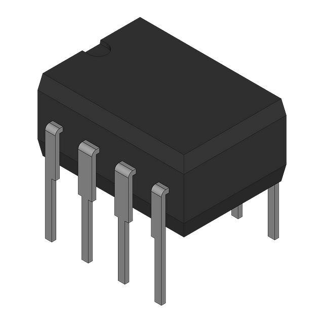


 工商网监
湘ICP备2023018690号
工商网监
湘ICP备2023018690号
