UMFT260EV1A Datasheet
Version 1.0
D oc ument Reference N o.: FT _001277
C learance N o.: FT DI# 4 9 9
Future Technology
Devices International
UMFT260EV1A Datasheet
HID-class USB to
UART/I2C Module
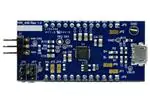
UMFT260EV1A is an FT260 DIP development module.
1 Introduction
1.1
The UMFT260EV1A is a development module for
FTDI’s FT260, HID-class USB to UART/I2C Bridge
IC. The UMFT260EV1A is ideal for development
purposes to quickly prove functionality of adding
USB to a target design.
The UMFT260EV1A is built with a FT260; many of the
features of the FT260 can be utilized with this module.
For further details of FT260 features, please refer to
the FT260 datasheet, DS_FT260, is available at
http://www.ftdichip.com/FT260.
The UMFT260EV1A is a module which is designed
to plug into a standard 0.8” wide 24 pin DIP
socket. The USB connection to a host system is
via a Micro USB-B connector.
In addition to the features listed in the FT260
datasheet, the UMFT260EV1A has the following
features:
All components used, including the FT260 are Pbfree (RoHS compliant).
PCB assembly module is designed to fit a standard
20.32mm (0.8”) wide 24 pin DIP socket. Pins are
on a 2.54mm (0.1”) pitch.
An on-board Micro USB-B type connector allows
modules to be connected to a host system via a
standard USB A to Micro B cable.
On-board I2C 2kbits EEPROM (address:0x50) to
contain FT260 configuration settings and vendor
specific parameters (I2C pull-high circuit is
implemented as default)
Jumpers for selecting the FT260 HID interfaces
configuration
Solder jumpers for configuring the FT260Q to be
in USB Bus powered or Self powered modes.
Features
N either the whole nor any part of the information c ontained in, or the product described in this manual, may be adapted or
reproduced in any material or elec tronic form without the prior written c onsent of the c opyright holder. T his product and its
doc umentation are s upplied on an as- is basis and no warranty as to their s uitability for any partic ular purpos e is either made or
implied. Future T ec hnology Devic es I nternational L td will not accept any claim for damages hows oever arising as a res ult of u se or
failure of this produc t. Y our statutory rights are not affecte d. T his produc t or any variant of it is not intended for us e in any
medical appliance, device or s ystem in whic h the failure of the produc t might reasonably be expected to res ult in pers onal in jury.
T his doc ument provides preliminary information that may b e s ubject to c hange without notice. N o freedom to use patents or other
intellec tual property rights is implied by the publication of this doc ument. Future Tec hnology D evices I nternational L td, U ni t 1 , 2
Seaward P lac e, C enturion Business P ark, G lasgow G 4 1 1HH U nited Kingdom. Sc otland Registered C ompany N umber: SC 136640
Copyright © Future Technology Devices International Limited
1
�UMFT260EV1A Datasheet
Version 1.0
D oc ument Reference N o.: FT _001277
C learance N o.: FT DI# 4 9 9
Table of Contents
1 Introduction ................................................................. 1
1.1
Features ................................................................................ 1
2 Driver Support .............................................................. 3
3 Ordering Information .................................................... 4
4 UMFT260EV1A Signals................................................... 5
4.1
UMFT260EV1A Pin Out............................................................ 5
4.2
JP1/JP5/JP6 Signal Descriptions ............................................ 6
4.3
Jumper Descriptions .............................................................. 8
5 Module Configurations .................................................. 9
5.1
Power Configuration .............................................................. 9
A.
Bus Powered Configuration .......................................................................9
B.
Self Powered configuration .......................................................................9
5.2
I/O Voltage Level Configuration ............................................10
A.
Internal Regulator(3.3V) Configuration ..................................................... 10
B.
External Power Source Configuration ........................................................ 10
5.3
I2C Bus Pull-up Configuration ................................................11
5.4
On-board I2C EEPROM Configuration ......................................11
5.5
Programming the FT260 On-Chip eFUSE.................................11
5.6
Power consumption...............................................................12
6 Module Dimensions ..................................................... 13
7 UMFT260EV1A Module Circuit Schematic...................... 14
8 Contact Information.................................................... 15
Appendix A – References ................................................. 14
Document References ...................................................................14
Acronyms and Abbreviations .........................................................14
Appendix B – List of Figures and Tables............................ 15
List of Figures ...............................................................................15
List of Tables ................................................................................15
Appendix C – Revision History.......................................... 16
Copyright © Future Technology Devices International Limited
2
�UMFT260EV1A Datasheet
Version 1.0
D oc ument Reference N o.: FT _001277
C learance N o.: FT DI# 4 9 9
2 Driver Support
Standard Human Interface Device (HID) Driver support for the FT260 USB Device is available from
the following OS:
Windows 10 32,64-bit
Windows 8.1 32,64-bit
Windows 8 32,64-bit
Windows 7 32,64-bit
Windows Vista and Vista 64-bit
Windows XP and XP 64-bit
Windows Server 2008, 2003, 2000
Windows Embedded Operating Systems
Mac OS X
Linux
Copyright © Future Technology Devices International Limited
3
�UMFT260EV1A Datasheet
Version 1.0
D oc ument Reference N o.: FT _001277
C learance N o.: FT DI# 4 9 9
3 Ordering Information
Module Code
UMFT260EV1A
Utilised IC Code
FT260Q
Description
FT260Q Development module.
Copyright © Future Technology Devices International Limited
4
�UMFT260EV1A Datasheet
Version 1.0
D oc ument Reference N o.: FT _001277
C learance N o.: FT DI# 4 9 9
4 UMFT260EV1A Signals
4.1
UMFT260EV1A Pin Out
Figure 4.1 Module Pin Out
Figure 4.1 illustrates the signals available on the DIP pins. The information relating to the on-board
jumpers will be described later in this chapter.
Copyright © Future Technology Devices International Limited
5
�UMFT260EV1A Datasheet
Version 1.0
D oc ument Reference N o.: FT _001277
4.2
C learance N o.: FT DI# 4 9 9
JP1/JP5/JP6 Signal Descriptions
Connector
Name
Type
J1-1
GND
Ground
Ground 0 volts.
J1-2
FSOURCE
Power
FT260 FSOURCE Pin (input).
J1-3
GND
Ground
Ground 0 volts.
Pin
Description
Table 4.1 JP1 Pin Out Description
Connector
Name
Type
JP5-1
VBUS
Power
JP5-2
VCCIN
Power
JP5-3
GND
Ground
JP5-4
RESETN
Signal
FT260 RESETN Pin.
JP5-5
BCD_DET
Signal
FT260 DIO12 Pin.
JP5-6
TXACTIVE
Signal
FT260 DIO0 Pin.
JP5-7
GND
Ground
Ground 0 volts.
JP5-8
RTSN
Signal
FT260 DIO1 Pin.
JP5-9
CTSN
Signal
FT260 DIO2 Pin.
JP5-10
RXD
Signal
FT260 DIO3 Pin.
JP5-11
TXD
Signal
FT260 DIO4 Pin.
JP5-12
GND
Ground
Ground 0 volts.
Pin
Description
USB VBUS Power pin (output). The USB VBUS is connected
to the FT260 VCCIN Pin through JP2 as default
FT260 VCCIN Pin (input). The FT260 VCCIN is connected to
the USB VBUS Pin through JP2 as default
Ground 0 volts.
Table 4.2 JP5 Pin Out Description
Copyright © Future Technology Devices International Limited
6
�UMFT260EV1A Datasheet
Version 1.0
D oc ument Reference N o.: FT _001277
Connector
Pin
JP6-1
Name
Type
VOUT3V3
Power
C learance N o.: FT DI# 4 9 9
Description
FT260 VOUT3V3 Pin (output). The FT260 VOUT3V3 pin is
connected to the FT260 VCCIO pin through JP1 as default
FT260 VCCIO Pin (input). The FT260 VCCIO pin is
JP6-2
VCCIO
Power
connected to the FT260 VOUT3V3 Pin through JP1 as
default
JP6-3
DSRN
Signal
FT260 DIO13 Pin.
JP6-4
RI
Signal
FT260 DIO11 Pin.
JP6-5
DCD
Signal
FT260 DIO10 Pin.
JP6-6
DTRN
Signal
FT260 DIO9 Pin.
JP6-7
GND
Ground
Ground 0 volts.
JP6-8
IO3
Signal
FT260 DIO8 Pin.
JP6-9
IO2
Signal
FT260 DIO7 Pin.
JP6-10
IO1
Signal
JP6-11
IO0
Signal
JP6-12
GND
Ground
FT260 DIO6 Pin. The on-board I2C bus pull-up circuit is
connected as default(JP4 shorted)
FT260 DIO5 Pin. The on-board I2C bus pull-up circuit is
connected as default(JP3 shorted )
Ground 0 volts.
Table 4.3 JP6 Pin Out Description
Copyright © Future Technology Devices International Limited
7
�UMFT260EV1A Datasheet
Version 1.0
D oc ument Reference N o.: FT _001277
4.3
C learance N o.: FT DI# 4 9 9
Jumper Descriptions
UMFT260EV1A provides two kinds of jumper: Solder jumper and Shunt jumper.
Jumper
Setting
Status
Description
Short
Default
VCCIO is connected to VOUT3V3. All I/O of the FT260 are
working at 3.3V.
Open
Non-Default
Short
Default
Open
Non-Default
Self-Powered mode. This setting removes the connection
between VBUS and VCCIN. The VCCIN (JP5-2) should be
connected to the external 5V source.
Short
Default
The on-board I2C bus pull-up circuit is connected to IO0
(JP6-11)
Open
Non-Default
The on-board I2C bus pull-up circuit is removed from IO0
(JP6-11)
Short
Default
The on-board I2C bus pull-up circuit is connected to IO1
(JP6-10)
Open
Non-Default
The on-board I2C bus pull-up circuit is removed from IO1
(JP6-10)
Short
Default
JP1
JP2
JP3
JP4
JP8
Open
VCCIO is disconnected from VOUT3V3. The VCCIO should
be connected to external power source, e.g. 1.8/2.5V/3.3V.
Bus-Powered mode. This setting creates a connection
between VBUS and VCCIN.
The on-board I2C EEPROM is enabled
Non-Default
The on-board I2C EEPROM is disabled
Table 4.4 Solder Jumper Description
Pin No.
Name
Type
Description
JP7-1
VCCIO
Power
Set DCNF0 High.
JP7-2
DCNF0
Signal
FT260 chip configuration selection bit 0. Refer to the FT260
datasheet
JP7-3
GND
Pin No.
Name
Type
JP9-1
VCCIO
Power
Set DCNF1 High.
JP9-2
DCNF1
Signal
FT260 chip configuration selection bit 1. Refer to the FT260
datasheet
JP9-3
GND
Ground
Set DCNF0 Low (Default).
Table 4.5 JP7 Pin Description
Description
Ground
Set DCNF1 Low (Default).
Table 4.6 JP9 Pin Description
Copyright © Future Technology Devices International Limited
8
�UMFT260EV1A Datasheet
Version 1.0
D oc ument Reference N o.: FT _001277
C learance N o.: FT DI# 4 9 9
5 Module Configurations
5.1
Power Configuration
A. Bus Powered Configuration
Figure 5.1 Bus Powered Configuration: JP2 shorted
Figure 5.1 illustrates the UMFT260EV1A module in a typical USB bus powered configuration. This is done
by soldering the jumpers at JP1 and JP2. The UMFT260EV1A is shipped in this configuration as default.
B. Self Powered configuration
Figure 5.2 Self Powered Configuration: JP1 shorted and JP2 opened
Figure 5.2 illustrates the UMFT260EV1A module in a typical USB self powered configuration. In this case,
the solder at jumpers JP2 is removed and the external VCC (5V) is connected to module JP5 Pin2 (VCCIN).
Warning: There should never be more than one power output supplying power to the same net at any
one time. Shorting JP2 will cause a direct connection between two different power supplies, when a selfpowered set-up is applied and the USB bus is connected resulting in the potential for damage to the
module and other connected circuitry.
Copyright © Future Technology Devices International Limited
9
�UMFT260EV1A Datasheet
Version 1.0
D oc ument Reference N o.: FT _001277
5.2
C learance N o.: FT DI# 4 9 9
I/O Voltage Level Configuration
A. Internal Regulator(3.3V) Configuration
Figure 5.3 I/O voltage level with internal regulator: JP1 shorted
Figure 5.3 shows a configuration of USB bus powered and using the internal regulator for I/O voltage
levels. The solder jumper JP1 allows the FT260 to use the internal 3.3V regulator. The FT260 VCCIO pin
is connected to the FT260 VOUT3V3 pin through JP1.
B. External Power Source Configuration
Figure 5.4 I/O voltage level with external power source: JP1 opened
Figure 5.4 shows a configuration of using an external power source for the FT260 IO supply voltage. After
removing the solder at JP1 on the UMFT260EV1A module, the FT260 can apply the external power source
to the FT260 VCCIO pin through JP6 Pin 1. FT260 VCCIO pin can accept 3.3V/2.5V/1.8V voltage levels for
all the FT260 I/O pins.
Copyright © Future Technology Devices International Limited
10
�UMFT260EV1A Datasheet
Version 1.0
D oc ument Reference N o.: FT _001277
5.3
C learance N o.: FT DI# 4 9 9
I2C Bus Pull-up Configuration
Figure 5.5 Enable I2C interface pull high: JP3 shorted and JP4 shorted
Figure 5.5 illustrates the location of JP3 and JP4 (marked in red) for I2C bus pull-up configuration. Since
the default function of IO0 and IO1 is the I2C bus, the UMFT260EV1A connects the pull-up circuit to the
I2C bus as default. If the IO0 and IO1 are configured as GPIO features, the user needs to remove the
pull-up circuit by unsoldering JP3 and JP4.
5.4
On-board I2C EEPROM Configuration
Figure 5.6 Enable on-board I2C EEPROM: JP8 shorted
Figure 5.6 illustrates the location of JP8 (marked in red) for I2C EEPROM configuration. The FT260 allows
chip configuration settings and vendor specific parameters to be stored in an external EEPROM. The
UMFT260EV1A populates the 2kbits EEPROM with address 0x50. If an on-board EEPROM is not required,
de-solder JP8 to disable the EEPROM.
The EEPROM is programmed before shipping. Refer to the FT260 datasheet for default values.
5.5
Programming the FT260 On-Chip eFUSE
Figure 5.7 Apply external voltage 3.8V to J1 Pin 2
Copyright © Future Technology Devices International Limited
11
�UMFT260EV1A Datasheet
Version 1.0
D oc ument Reference N o.: FT _001277
C learance N o.: FT DI# 4 9 9
The FT260 On-Chip eFUSE can be programmed through the USB HID interface. For the UMFT260EV1A
module, UMFTPD3A is required to program the FT260 eFUSE. UMFTPD3A will supply the 3.8V
programming voltage to the FT260 FSOURCE pin through UMFT260EV1A module J1 Pin 2.
The datasheet of UMFTPD3A module is available at this link.
http://www.ftdichip.com/Support/Documents/DataSheets/Modules/DS_UMFTPD3A.pdf
5.6
Power consumption
Parameter
Description
Mini.
Typical
Max.
Units
Conditions
IVBUS1
VBUS Operating
Current
-
24.2
-
mA
VBUS Powered,
Function Mode
IVBUS2
VBUS Operating
Current
-
4.4
-
mA
VBUS Powered,
IDLE Mode
IVBUS3
VBUS Operating
Current
-
400
-
μA
VBUS Powered,
Suspend Mode
Table 5.1 Power Consumption
Copyright © Future Technology Devices International Limited
12
�UMFT260EV1A Datasheet
Version 1.0
D oc ument Reference N o.: FT _001277
C learance N o.: FT DI# 4 9 9
6 Module Dimensions
Figure 6.1 UMFT260EV1A Module Dimensions
All dimensions are given in millimetres.
The UMFT260EV1A module exclusively uses lead free components, and is fully compliant with European
Union directive 2002/95/EC.
Copyright © Future Technology Devices International Limited
13
�UMFT260EV1A Datasheet
Version 1.0
D oc ument Reference N o.: FT _001277
C learance N o.: FT DI# 4 9 9
7 UMFT260EV1A Module Circuit Schematic
Figure 7.1 Module Circuit Schematic
Copyright © Future Technology Devices International Limited
14
�UMFT260EV1A Datasheet
Version 1.0
D oc ument Reference N o.: FT _001277
C learance N o.: FT DI# 4 9 9
8 Contact Information
Head Office – Glasgow, UK
Branch Office – Tigard, Oregon, USA
Unit 1, 2 Seaward Place, Centurion Business Park
Glasgow G41 1HH
United Kingdom
Tel: +44 (0) 141 429 2777
Fax: +44 (0) 141 429 2758
7130 SW Fir Loop
Tigard, OR 97223
USA
Tel: +1 (503) 547 0988
Fax: +1 (503) 547 0987
E-mail (Sales)
E-mail (Support)
E-mail (General Enquiries)
E-Mail (Sales)
E-Mail (Support)
E-Mail (General Enquiries)
sales1@ftdichip.com
support1@ftdichip.com
admin1@ftdichip.com
Branch Office – Taipei, Taiwan
2F, No. 516, Sec. 1, NeiHu Road
Taipei 114
Taiwan , R.O.C.
Tel: +886 (0) 2 8797 1330
Fax: +886 (0) 2 8751 9737
E-mail (Sales)
E-mail (Support)
E-mail (General Enquiries)
tw.sales1@ftdichip.com
tw.support1@ftdichip.com
tw.admin1@ftdichip.com
us.sales@ftdichip.com
us.support@ftdichip.com
us.admin@ftdichip.com
Branch Office – Shanghai, China
Room 1103, No. 666 West Huaihai Road,
Shanghai, 200052
C hina
Tel: +86 (0)21 6235 1596
Fax: +86 (0)21 6235 1595
E-mail (Sales)
E-mail (Support)
E-mail (General Enquiries)
cn.sales@ftdichip.com
cn.support@ftdichip.com
cn.admin@ftdichip.com
Web Site
http://ftdichip.com
Distributor and Sales Representatives
Please visit the Sales Network page of the FTDI Web site for the contact details of our distributor(s) and sales
representative(s) in your country.
System and equipment manufac turers and des igners are res pons ible to ens ure that their sys tems , and any Future T ec hnology Dev ices
I nternational Ltd (FTDI ) devic es incorporated in their s ystems , meet all applicable safety, regulatory and sys tem-level performanc e
requirements . All application- related information in this doc ument (including applic ation desc riptions , s uggested FTDI devic es and other
materials ) is provided for reference only. While FTDI has taken c are to ass ure it is acc urate, this information is s ubjec t to c us tomer
c onfirmation, and FTDI disclaims all liability for sys tem designs and for any applic ations assis tanc e p rovided by FTDI . Us e of FTDI
devic es in life s upport and/or safety applications is entirely at the us er’s risk, and the us er agrees to defend, indemnify a nd hold
harmless FTDI from any and all damages , claims , s uits or expens e resulting from s uch use. T his doc ument is s ubject to change without
notice. N o freedom to use patents or other intellec tual property rights is implied by the publication of this doc ument. N either the whole
nor any part of the information c ontained in, or the product desc ribed in this document, may be adapted or reproduced in any material
or elec tronic form without the prior written c onsent of the c opyright holder. Future Tec hnology D evices I nternational L td, U n it 1 , 2
Seaward P lac e, C enturion Business P ark, G lasgow G 4 1 1HH, U nited King dom. Sc otland Registered Company N umber: SC136640
Copyright © Future Technology Devices International Limited
15
�UMFT260EV1A
D oc ument Reference N o.: FT _001277
Datasheet
Version 1.0
C learance N o.: FT DI# 4 9 9
Appendix A – References
Document References
Application Notes
AN_394 User Guide for FT260
AN_395 User Guide for LibFT260
AN_124 User Guide for FTDI FT_Prog Utility
AN_184 FTDI Device Input Output Pin States
AN_175 Battery Charger Detection Over USB with FT-X Devices
Technical Notes
TN_100 USB Vendor ID/Product ID Guidelines
TN_111 What is UART
Datasheets
DS_FT260
UMFTPD3A Program Module Datasheet
FT_PROG Utility
http://www.ftdichip.com/Support/Utilities.htm#FT_Prog
Related Document or Specification
http://i2c2p.twibright.com/spec/i2c.pdf
https://msdn.microsoft.com/en-us/library/windows/hardware/dn642101(v=vs.85).aspx
https://msdn.microsoft.com/en-US/library/jj131705(v=vs.85).aspx
Acronyms and Abbreviations
Terms
Description
eFUSE
Electrical poly fuse
GPIO
General purpose I/O
HID
Human interface device
I2C
Inter integrated Circuit
UART
USB
Universal Asynchronous Receiver/Transmitter
Universal Serial Bus
Copyright © Future Technology Devices International Limited
14
�UMFT260EV1A
D oc ument Reference N o.: FT _001277
Datasheet
Version 1.0
C learance N o.: FT DI# 4 9 9
Appendix B – List of Figures and Tables
List of Figures
Figure 4.1 Module Pin Out ...................................................................................................................... 5
Figure 5.1 Bus Powered Configuration: JP2 shorted................................................................................. 9
Figure 5.2 Self Powered Configuration: JP1 shorted and JP2 opened ....................................................... 9
Figure 5.3 I/O voltage level with internal regulator: JP1 shorted ........................................................... 10
Figure 5.4 I/O voltage level with external powe r source: JP1 opened .................................................... 10
Figure 5.5 Enable I2C interface pull high: JP3 shorted and JP4 shorted .................................................. 11
Figure 5.6 Enable on-board I2C EEPROM: JP8 shorted ........................................................................... 11
Figure 5.7 Apply external voltage 3.8V to J1 Pin 2 ................................................................................ 11
Figure 6.1 UMFT260EV1A Module Dimensions ....................................................................................... 13
Figure 7.1 Module Circuit Schematic ..................................................................................................... 14
List of Tables
Table 4.1 JP1 Pin Out Description ........................................................................................................... 6
Table 4.2 JP5 Pin Out Description ........................................................................................................... 6
Table 4.3 JP6 Pin Out Description ........................................................................................................... 7
Table 4.4 Solder Jumper Description....................................................................................................... 8
Table 4.5 JP7 Pin Description .................................................................................................................. 8
Table 4.6 JP9 Pin Description .................................................................................................................. 8
Table 5.1 Power Consumption .............................................................................................................. 12
Copyright © Future Technology Devices International Limited
15
�UMFT260EV1A
D oc ument Reference N o.: FT _001277
Datasheet
Version 1.0
C learance N o.: FT DI# 4 9 9
Appendix C – Revision History
Document Title:
UMFT260EV1A Datasheet
Document Reference No.:
FT_001277
Clearance No.:
FTDI# 499
Product Page:
http://www.ftdichip.com
Document Feedback:
Send Feedback
Revision
Changes
Date
Version 1.0
Initial Release
2016-04-27
Copyright © Future Technology Devices International Limited
16
�


 工商网监
湘ICP备2023018690号
工商网监
湘ICP备2023018690号
