IDT6116SA
IDT6116LA
CMOS Static RAM
16K (2K x 8-Bit)
Features
◆
◆
◆
◆
◆
◆
◆
◆
◆
Description
High-speed access and chip select times
– Military: 20/25/35/45/55/70/90/120/150ns (max.)
– Industrial: 20/25/35/45ns (max.)
– Commercial: 15/20/25/35/45ns (max.)
Low-power consumption
Battery backup operation
– 2V data retention voltage (LA version only)
Produced with advanced CMOS high-performance
technology
CMOS process virtually eliminates alpha particle soft-error
rates
Input and output directly TTL-compatible
Static operation: no clocks or refresh required
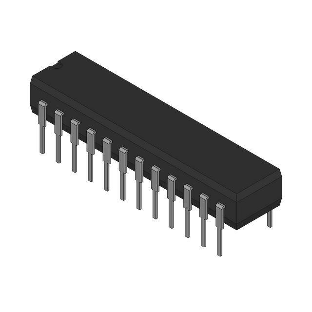
Available in ceramic and plastic 24-pin DIP, 24-pin Thin Dip,
24-pin SOIC and 24-pin SOJ
Military product compliant to MIL-STD-833, Class B
The IDT6116SA/LA is a 16,384-bit high-speed static RAM
organized as 2K x 8. It is fabricated using IDT's high-performance,
high-reliability CMOS technology.
Access times as fast as 15ns are available. The circuit also offers a
reduced power standby mode. When CS goes HIGH, the circuit will
automatically go to, and remain in, a standby power mode, as long
as CS remains HIGH. This capability provides significant system level
power and cooling savings. The low-power (LA) version also offers a
battery backup data retention capability where the circuit typically
consumes only 1µW to 4µW operating off a 2V battery.
All inputs and outputs of the IDT6116SA/LA are TTL-compatible. Fully
static asynchronous circuitry is used, requiring no clocks or refreshing
for operation.
The IDT6116SA/LA is packaged in 24-pin 600 and 300 mil plastic or
ceramic DIP, 24-lead gull-wing SOIC, and 24-lead J-bend SOJ providing
high board-level packing densities.
Military grade product is manufactured in compliance to the latest
version of MIL-STD-883, Class B, making it ideally suited to military
temperature applications demanding the highest level of performance and
reliability.
Functional Block Diagram
A0
V CC
128 X 128
MEMORY
ARRAY
ADDRESS
DECODER
GND
A 10
I/O 0
I/O CONTROL
INPUT
DATA
CIRCUIT
I/O 7
,
CS
OE
WE
CONTROL
CIRCUIT
3089 drw 01
NOVEMBER 2006
1
©2006 Integrated Device Technology, Inc.
DSC-3089/06
�IDT6116SA/LA
CMOS Static RAM 2K (16K x 8-Bit)
Military, Commercial, and Industrial Temperature Ranges
Pin Configurations
Capacitance (TA = +25°C, f = 1.0 MHZ)
Symbol
A7
A6
A5
A4
A3
A2
A1
A0
I/O 0
I/O 1
I/O 2
GND
1
2
3
4
5
6
7
8
9
10
11
12
P24-2
P24-1
D24-2
D24-1
SO24-2
SO24-4
24
23
22
21
20
19
18
17
16
15
14
13
VCC
A8
A9
WE
OE
A10
CS
I/O 7
I/O 6
I/O 5
I/O 4
I/O3
Parameter(1)
Conditions
Max.
Unit
CIN
Input Capacitance
V IN = 0V
8
pF
CI/O
I/O Capacitance
VOUT = 0V
8
pF
3089 tbl 03
NOTE:
1. This parameter is determined by device characterization, but is not production
tested.
,
Absolute Maximum Ratings(1)
3089 drw 02
Symbol
DIP/SOIC/SOJ
Top View
(2)
Pin Description
Rating
Com'l.
Mil.
Unit
-0.5 to +7.0
-0.5 to +7.0
V
VTERM
Terminal Voltage
with Respect
to GND
TA
Operating
Temperature
0 to +70
-55 to +125
o
C
TBIAS
Temperature
Under Bias
-55 to +125
-65 to +135
o
C
TSTG
Storage Temperature
-55 to +125
-65 to +150
o
C
Name
Description
A0 - A10
Address Inputs
I/O0 - I/O7
Data Input/Output
PT
Power Dissipation
1.0
1.0
W
CS
Chip Select
IOUT
DC Output Current
50
50
mA
WE
Write Enable
OE
Output Enable
VCC
Power
GND
Ground
3089 tbl 04
NOTES:
1. Stresses greater than those listed under ABSOLUTE MAXIMUM RATINGS
may cause permanent damage to the device. This is a stress rating only and
functional operation of the device at these or any other conditions above those
indicated in the operational sections of this specification is not implied. Exposure
to absolute maximum rating conditions for extended periods may affect
reliability.
2. VTERM must not exceed VCC +0.5V.
3089 tbl 01
Truth Table(1)
CS
OE
WE
I/O
Standby
H
X
X
High-Z
Read
L
L
H
DATAOUT
Read
L
H
H
High-Z
Write
L
X
L
DATA IN
Mode
NOTE:
1. H = VIH, L = VIL, X = Don't Care.
3089 tbl 02
2
�IDT6116SA/LA
CMOS Static RAM 2K (16K x 8-Bit)
Military, Commercial, and Industrial Temperature Ranges
Recommended Operating
Temperature and Supply Voltage
Symbol
Ambient
Temperature
GND
Vcc
Military
-55OC to +125OC
0V
5.0V ± 10%
Industrial
-40OC to +85OC
0V
5.0V ± 10%
0OC to +70OC
0V
5.0V ± 10%
Grade
Commercial
Recommended DC
Operating Conditions
Parameter
VCC
Supply Voltage
GND
Ground
VIH
Input High Voltage
VIL
Min.
Typ.
4.5
5.0
0
2.2
(1)
Input Low Voltage
-0.5
Max.
Unit
(2)
5.5
V
0
0
V
3.5
VCC +0.5
V
____
0.8
V
3089 tbl 05
NOTES:
1. VIL (min.) = –3.0V for pulse width less than 20ns, once per cycle.
2. VIN must not exceed VCC +0.5V.
3089 tbl 06
DC Electrical Characteristics
(VCC = 5.0V ± 10%)
IDT6116SA
Symbol
|ILI|
|ILO|
VOL
VOH
Parameter
Input Leakage Current
Output Leakage Current
Output Low Voltage
Output High Voltage
Test Conditions
Min.
Max.
Min.
Max.
Unit
10
5
____
5
2
µA
10
5
____
____
5
2
µA
____
____
0.4
____
0.4
V
2.4
____
2.4
____
V
VCC = Max.,
VIN = GND to VCC
MIL.
COM'L.
____
VCC = Max., CS = VIH,
VOUT = GND to V CC
MIL.
COM'L.
____
____
IOL = 8mA, VCC = Min.
IOH = -4mA, VCC = Min.
IDT6116LA
____
3089 tbl 07
DC Electrical Characteristics(1)
(VCC = 5.0V ± 10%, VLC = 0.2V, VHC = VCC - 0.2V)
6116SA15
Symbol
ICC1
ICC2
ISB
ISB1
6116SA20
6116LA20
6116SA25
6116LA25
6116SA35
6116LA35
Power
Com'l
Only
Com'l
& Ind
Mil
Com'l
& Ind
Mil
Com'l.
& Ind.
Mil
Unit
Operating Power Supply Current
CS < VIL, Outputs Open
V CC = Max., f = 0
SA
105
105
130
100
90
100
90
mA
LA
95
95
120
95
85
95
85
Dynamic Operating Current
CS < VIL, Outputs Open
V CC = Max., f = fMAX(2)
SA
150
130
150
120
135
100
115
LA
140
120
140
110
125
95
105
Standby Power Supply Current
(TTL Level)
CS > VIH, Outputs Open
V CC = Max., f = fMAX(2)
SA
40
40
50
40
45
25
35
LA
35
35
45
35
40
25
30
Full Standby Power Supply Current
(CMOS Level)
CS > VHC, VCC = Max.,
V IN < V LC or VIN > VHC, f = 0
SA
2
2
10
2
10
2
10
LA
0.1
0.1
0.9
0.1
0.9
0.1
0.9
Parameter
NOTES:
1. All values are maximum guaranteed values.
2. fMAX = 1/tRC, only address inputs are cycling at fMAX, f = 0 means address inputs are not changing.
6.42
3
mA
mA
mA
3089 tbl 08
�IDT6116SA/LA
CMOS Static RAM 2K (16K x 8-Bit)
Military, Commercial, and Industrial Temperature Ranges
DC Electrical Characteristics(1) (continued)
(VCC = 5.0V ± 10%, VLC = 0.2V, VHC = VCC - 0.2V)
6116SA45
6116LA45
6116SA55
6116LA55
6116SA70
6116LA70
6116SA90
6116LA90
6116SA120
6116LA120
6116SA150
6116LA150
Symbol
Parameter
Power
Com'l
& Ind
Mil
Mil Only
Mil Only
Mil Only
Mil Only
Mil Only
Unit
ICC1
Operating Power Supply
Current, CS < VIL,
Outputs Open
VCC = Max., f = 0
SA
100
90
90
90
90
90
90
mA
LA
95
85
85
85
85
85
85
Dynamic Operating
Current, CS < VIL,
Outputs Open
VCC = Max., f = fMAX(2)
SA
100
100
100
100
100
100
90
LA
90
95
90
90
85
85
85
Standby Power Supply
Current (TTL Level)
CS > VIH, Outputs Open
VCC = Max., f = fMAX(2)
SA
25
25
25
25
25
25
25
LA
20
20
20
20
25
15
15
SA
2
10
10
10
10
10
10
LA
0.1
0.9
0.9
0.9
0.9
0.9
0.9
ICC2
ISB
ISB1
Full Standby Power
Supply Current (CMOS
Level), CS > V HC,
VCC = Max., V IN < V LC
or VIN > VHC, f = 0
mA
mA
mA
3089 tbl 09
NOTES:
1. All values are maximum guaranteed values.
2. fMAX = 1/tRC, only address inputs are toggling at fMAX, f = 0 means address inputs are not changing.
Data Retention Characteristics Over All Temperature Ranges
(LA Version Only) (VLC = 0.2V, VHC = VCC – 0.2V)
Typ. (1)
VCC @
Symbol
Parameter
V DR
VCC for Data Retention
ICCDR
Data Retention Current
tCDR(3)
Chip Deselect to Data
Retention Time
tR(3)
Operation Recovery Time
IILII
Input Leakage Current
Max.
VCC @
Test Condition
Min.
2.0V
3.0V
2.0V
3.0V
Unit
____
2.0
____
____
____
____
V
____
0.5
0.5
1.5
1.5
200
20
300
30
µA
____
0
____
____
____
ns
tRC(2)
____
____
____
____
ns
____
____
____
2
2
µA
MIL.
COM'L.
CS > VHC
VIN > VHC or < VLC
NOTES:
1. TA = + 25°C
2. tRC = Read Cycle Time.
3. This parameter is guaranteed by device characterization, but is not production tested.
4
____
3089 tbl 10
�IDT6116SA/LA
CMOS Static RAM 2K (16K x 8-Bit)
Military, Commercial, and Industrial Temperature Ranges
Low VCC Data Retention Waveform
DATA RETENTION MODE
VCC
VDR ≥ 2V
4.5V
4.5V
tCDR
tR
VDR
CS
,
VIH
VIH
3089 drw 03
AC Test Conditions
Input Pulse Levels
GND to 3.0V
Input Rise/Fall Times
5ns
Input Timing Reference Levels
1.5V
Output Reference Levels
1.5V
AC Test Load
See Figures 1 and 2
3089 tbl 11
5V
5V
480Ω
480Ω
DATAOUT
DATAOUT
255Ω
255Ω
30pF*
5pF*
,
3089 drw 05
3089 drw 04
Figure 1. AC Test Load
Figure 2. AC Test Load
(for tOLZ, tCLZ, tOHZ , tWHZ, tCHZ & tOW)
*Including scope and jig.
6.42
5
,
�IDT6116SA/LA
CMOS Static RAM 2K (16K x 8-Bit)
Military, Commercial, and Industrial Temperature Ranges
AC Electrical Characteristics (VCC = 5V ± 10%, All Temperature Ranges)
6116SA15(1)
Symbol
Parameter
6116SA20
6116LA20
6116SA25
6116LA25
6116SA35
6116LA35
Min.
Max.
Min.
Max.
Min.
Max.
Min.
Max.
Unit
Read Cycle
tRC
Read Cycle Time
15
____
20
____
25
____
35
____
ns
tAA
Address Access Time
____
15
____
19
____
25
____
35
ns
tACS
Chip Select Access Time
____
15
____
20
____
25
____
35
ns
tCLZ(3)
Chip Select to Output in Low-Z
5
____
5
____
5
____
5
____
ns
____
10
____
10
____
13
____
20
ns
tOE
Output Enable to Output Valid
tOLZ(3)
Output Enable to Output in Low-Z
0
____
0
____
5
____
5
____
ns
tCHZ(3)
Chip Dese lect to Output in High-Z
____
10
____
11
____
12
____
15
ns
tOHZ(3)
Output Disable to Output in High-Z
____
8
____
8
____
10
____
13
ns
5
____
5
____
5
____
ns
ns
tOH
Output Hold from Address Change
5
____
tPU(3)
Chip Select to Power Up Time
0
____
0
____
0
____
0
____
tPD(3)
Chip Desele ct to Power Down Time
____
15
____
20
____
25
____
35
ns
3089 tbl 12
AC Electrical Characteristics (VCC = 5V ± 10%, All Temperature Ranges) (continued)
6116SA45
6116LA45
Symbol
Parameter
6116SA55(2)
6116LA55(2)
6116SA70(2)
6116LA70(2)
6116SA90(2)
6116LA90(2)
6116SA120(2)
6116LA120(2)
6116SA150(2)
6116LA150(2)
Min.
Max.
Min.
Max.
Min.
Max.
Min.
Max.
Min.
Max.
Min.
Max.
Unit
Read Cycle Time
45
____
55
____
70
____
90
____
120
____
150
____
ns
tAA
Address Access Time
____
45
____
55
____
70
____
90
____
120
____
150
ns
tACS
Chip Select Access Time
____
45
____
50
____
65
____
90
____
120
____
150
ns
tCLZ(3)
Chip Select to Output in Low-Z
5
____
5
____
5
____
5
____
5
____
5
____
ns
____
25
____
40
____
50
____
60
____
80
____
100
ns
Read Cycle
tRC
tOE
Output Enable to Output Valid
tOLZ(3)
Output Enable to Output in Low-Z
5
____
5
____
5
____
5
____
5
____
5
____
ns
tCHZ(3)
Chip Dese lect to Output in High-Z
____
20
____
30
____
35
____
40
____
40
____
40
ns
tOHZ(3)
Output Disable to Output in High-Z
____
15
____
30
____
35
____
40
____
40
____
40
ns
tOH
Output Hold from Address Change
5
____
5
____
5
____
5
____
5
____
5
____
NOTES:
1. 0°C to +70°C temperature range only.
2. –55°C to +125°C temperature range only.
3. This parameter guaranteed with the AC Load (Figure 2) by device characterization, but is not production tested.
6
ns
3089 tbl 13
�IDT6116SA/LA
CMOS Static RAM 2K (16K x 8-Bit)
Military, Commercial, and Industrial Temperature Ranges
Timing Waveform of Read Cycle No. 1(1,3)
tRC
ADDRESS
tAA
tOH
OE
tOE
CS
tOLZ (5)
tACS
tCLZ
tCHZ
ICC
(5)
(5)
DATA
VALID
DATAOUT
VCC
Supply
Currents
tOHZ (5)
tPU
ISB
,
tPD
3089 drw 06
Timing Waveform of Read Cycle No. 2(1,2,4)
tRC
ADDRESS
tAA
tOH
tOH
DATAOUT
,
DATA VALID
PREVIOUS DATA VALID
3089 drw 07
Timing Waveform of Read Cycle No. 3(1,3,4)
CS
tCLZ (5)
tACS
tCHZ
DATAOUT
(5)
,
DATA VALID
3089 drw 08
NOTES:
1. WE is HIGH for Read cycle.
2. Device is continously selected, CS is LOW.
3. Address valid prior to or coincident with CS transition LOW.
4. OE is LOW.
5. Transition is measured ±500mV from steady state.
6.42
7
�IDT6116SA/LA
CMOS Static RAM 2K (16K x 8-Bit)
Military, Commercial, and Industrial Temperature Ranges
AC Electrical Characteristics (VCC = 5V ± 10%, All Temperature Ranges)
6116SA15(1)
Symbol
Parameter
6116SA20
6116LA20
6116SA25
6116LA25
6116SA35
6116LA35
Min.
Max.
Min.
Max.
Min.
Max.
Min.
Max.
Unit
15
____
20
____
25
____
35
____
ns
15
____
17
____
25
____
ns
Write Cycle
tWC
Write Cycle Time
tCW
Chip Select to End-of-Write
13
____
tAW
Address Valid to End-of-Write
14
____
15
____
17
____
25
____
ns
tAS
Address Set-up Time
0
____
0
____
0
____
0
____
ns
tWP
Write Pulse Width
12
____
12
____
15
____
20
____
ns
tWR
Write Recovery Time
0
____
0
____
0
____
0
____
ns
7
____
8
____
16
____
20
ns
(3)
tWHZ
Write to Output in High-Z
____
tDW
Data to Write Time Overlap
12
____
12
____
13
____
15
____
ns
tDH(4)
Data Hold from Write Time
0
____
0
____
0
____
0
____
ns
tOW(3,4)
Output Active from End-of-Write
0
____
0
____
0
____
0
____
ns
3089 tbl 14
AC Electrical Characteristics (VCC = 5V ± 10%, All Temperature Ranges) (continued)
6116SA45
6116LA45
Symbol
Parameter
6116SA55(2)
6116LA55(2)
6116SA70(2)
6116LA70(2)
6116SA90(2)
6116LA90(2)
6116SA120(2)
6116LA120(2)
6116SA150(2)
6116LA150(2)
Min.
Max.
Min.
Max.
Min.
Max.
Min.
Max.
Min.
Max.
Min.
Max.
Unit
45
____
55
____
70
____
90
____
120
____
150
____
ns
30
____
40
____
40
____
55
____
70
____
90
____
ns
30
____
45
____
65
____
80
____
105
____
120
____
ns
5
____
15
____
15
____
20
____
20
____
ns
Write Cycle
tWC
tCW
tAW
Write Cycle Time
Chip Select to End-of-Write
Address Valid to End-of-Write
tAS
Address Set-up Time
0
____
tWP
Write Pulse Width
25
____
40
____
40
____
55
____
70
____
90
____
ns
tWR
Write Recovery Time
0
____
5
____
5
____
5
____
5
____
10
____
ns
tWHZ(3)
Write to Output in High-Z
____
25
____
30
____
35
____
40
____
40
____
40
ns
25
____
30
____
30
____
35
____
40
____
ns
ns
tDW
Data to Write Time Overlap
20
____
tDH(4)
Data Hold from Write Time
0
____
5
____
5
____
5
____
5
____
10
____
tOW(3,4)
Output Active from End-of-Write
0
____
0
____
0
____
0
____
0
____
0
____
ns
3089 tbl 15
NOTES:
1. 0°C to +70°C temperature range only.
2. –55°C to +125°C temperature range only.
3. This parameter guaranteed with AC Load (Figure 2) by device characterization, but is not production tested.
4. The specification for tDH must be met by the device supplying write data to the RAM under all operation conditions. Although tDH and tOW values will vary over voltage
and temperature, the actual tDH will always be smaller than the actual tOW.
8
�IDT6116SA/LA
CMOS Static RAM 2K (16K x 8-Bit)
Military, Commercial, and Industrial Temperature Ranges
Timing Waveform of Write Cycle No. 1 (WE Controlled Timing)(1,2,5,7)
tWC
ADDRESS
tAW
CS
tAS
tWP (7)
tWR
(3)
tCHZ
(6)
WE
(6)
tWHZ
DATAOUT
PREVIOUS DATA VALID
tOW
(4)
tDW
DATAIN
(6)
DATA (4)
VALID
tDH
DATA VALID
3089 drw 09
,
Timing Waveform of Write Cycle No. 2 (CS Controlled Timing)(1,2,3,5,7)
tWC
ADDRESS
tAW
CS
tWR (3)
tAS
tCW
WE
tDW
DATAIN
tDH
DATA VALID
3089 drw 10
NOTES:
1. WE or CS must be HIGH during all address transitions.
2. A write occurs during the overlap of a LOW CS and a LOW WE.
3. tWR is measured from the earlier of CS or WE going HIGH to the end of the write cycle.
4. During this period, the I/O pins are in the output state and the input signals must not be applied.
5. If the CS LOW transition occurs simultaneously with or after the WE LOW transition, the outputs remain in the high-impedance state.
6. Transition is measured ±500mV from steady state.
7. OE is continuously HIGH. If OE is LOW during a WE controlled write cycle, the write pulse width must be the larger of tWP or (tWHZ + tDW) to allow the I/O drivers
to turn off and data to be placed on the bus for the required tDW. If OE is HIGH during a WE controlled write cycle, this requirement does not apply and the write pulse
is the specified tWP. For a CS controlled write cycle, OE may be LOW with no degradation to tCW.
6.42
9
,
�IDT6116SA/LA
CMOS Static RAM 2K (16K x 8-Bit)
Military, Commercial, and Industrial Temperature Ranges
Ordering Information — Military
IDT
6116
XX
XXX
X
X
Device Type
Power
Speed
Package
Process/
Temperature
Range
B
Military (-55°C to +125°C)
Compliant to MIL-STD-883, Class B
TD
D
300 mil CERDIP (D24-1)
600 mil CERDIP (D24-2)
20*
25*
35*
45
55
70
90
120
150**
SA
LA
,
Speed in nanoseconds
Standard Power
Low Power
*Available in 300 mil packaging only.
**Available in 600 mil packaging only.
3089 drw 11
Ordering Information — Commercial & Industrial
IDT
6116
XX
XXX
X
Device Type
Power
Speed
Package
X
X
Process/
Temperature
Range
Blank Commercial (0°C to +70°C)
Industrial (-40°C to +85°C)
I
G
Restricted hazardous substance device
TP
P
SO
Y
300 mil Plastic DIP (P24-1)
600 mil Plastic DIP (P24-2)
300 mil Small Outline IC, Gull-Wing Bend (SO24-2)
300 mil SOJ, J-Bend (SO24-4)
15*
20
25
35
45
Speed in nanoseconds
SA
LA
Standard Power
Low Power
*Available in commercial temperature range and standard power only.
3089 drw 12
10
,
�IDT6116SA/LA
CMOS Static RAM 2K (16K x 8-Bit)
Military, Commercial, and Industrial Temperature Ranges
Datasheet Document History
1/7/00
Pg. 1, 3, 4, 10
Pg. 9, 10
Pg. 11
08/09/00
02/01/01
12/30/03
03/31/05
11/15/06
Pg. 3,10
Pg. 10
Pg. 3
Pg.4
Updated to new format
Added Industrial Temperature range offerings
Separated ordering information into military, commercial, and industrial temperature range offerings
Added Datasheet Document History
Not recommended for new designs
Removed "Not recommended for new designs"
Corrected Industrial temp from -45C to -40C.
Added "Restricted hazardous substance device" to ordering information.
Changed power limits for commercial and industrial on speed grades 25ns and 35ns.
Changed powe limits for commercial and industrial on speed grade 45ns. Refer to
PCN SR-0602-02.
CORPORATE HEADQUARTERS
6024 Silver Creek Valley Road
San Jose, CA 95138
for SALES:
800-345-7015 or
408-284-8200
fax: 408-284-2775
www.idt.com
The IDT logo is a registered trademark of Integrated Device Technology, Inc.
6.42
11
for Tech Support:
ipchelp@idt.com
800-345-7015
�


 工商网监
湘ICP备2023018690号
工商网监
湘ICP备2023018690号
