IXYK120N120C3
IXYX120N120C3
1200V XPTTM IGBTs
GenX3TM
VCES =
IC110 =
VCE(sat)
tfi(typ) =
High-Speed IGBTs
for 20-50 kHz Switching
1200V
120A
3.20V
96ns
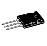
TO-264 (IXYK)
Symbol
Test Conditions
Maximum Ratings
VCES
VCGR
TJ = 25°C to 175°C
TJ = 25°C to 175°C, RGE = 1M
VGES
VGEM
1200
1200
V
V
Continuous
Transient
±20
±30
V
V
IC25
ILRMS
IC110
ICM
TC= 25°C (Chip Capability)
Terminal Current Limit
TC= 110°C
TC = 25°C, 1ms
240
160
120
700
A
A
A
A
IA
EAS
TC = 25°C
TC = 25°C
60
2
A
J
SSOA
(RBSOA)
VGE = 15V, TVJ = 150°C, RG = 1
Clamped Inductive Load
ICM = 240
VCE VCES
A
PC
TC = 25°C
1500
W
-55 ... +175
175
-55 ... +175
°C
°C
°C
300
260
°C
°C
1.13/10
Nm/lb.in
20..120 /4.5..27
N/lb
10
6
g
g
TJ
TJM
Tstg
TL
TSOLD
Maximum Lead Temperature for Soldering
1.6 mm (0.062in.) from Case for 10s
Md
Mounting Torque (TO-264)
FC
Mounting Force
Weight
TO-264
PLUS247
(PLUS247)
G
C
E
PLUS247 (IXYX)
G
BVCES
IC
= 250A, VGE = 0V
1200
VGE(th)
IC
= 500A, VCE = VGE
3.0
ICES
VCE = VCES, VGE = 0V
V
5.0
25 A
1.5 mA
TJ = 150C
IGES
VCE = 0V, VGE = 20V
VCE(sat)
IC
= IC110, VGE = 15V, Note 1
TJ = 150C
© 2013 IXYS CORPORATION, All Rights Reserved
V
100
2.55
3.40
3.20
nA
V
V
C
E
Tab
E
= Emitter
Tab = Collector
Features
Optimized for Low Switching Losses
Square RBSOA
International Standard Packages
Positive Thermal Coefficient of
Vce(sat)
Avalanche Rated
High Current Handling Capability
Advantages
Characteristic Values
Min.
Typ.
Max.
G
G = Gate
C = Collector
Symbol
Test Conditions
(TJ = 25C, Unless Otherwise Specified)
Tab
High Power Density
Low Gate Drive Requirement
Applications
High Frequency Power Inverters
UPS
Motor Drives
SMPS
PFC Circuits
Battery Chargers
Welding Machines
Lamp Ballasts
DS100451B(9/13)
�IXYK120N120C3
IXYX120N120C3
Symbol Test Conditions
(TJ = 25°C Unless Otherwise Specified)
Characteristic Values
Min.
Typ.
Max.
gfs
40
IC = 60A, VCE = 10V, Note 1
Cies
Coes
Cres
VCE = 25V, VGE = 0V, f = 1MHz
Qg(on)
Qge
Qgc
IC = IC110, VGE = 15V, VCE = 0.5 • VCES
td(on)
tri
Eon
td(off)
tfi
Eoff
td(on)
tri
Eon
td(off)
tfi
Eoff
Inductive load, TJ = 25°C
IC = 100A, VGE = 15V
VCE = 0.5 • VCES, RG = 1
Note 2
Inductive load, TJ = 150°C
IC = 100A, VGE = 15V
VCE = 0.5 • VCES, RG = 1
Note 2
RthJC
RthCS
TO-264 Outline
68
S
9850
580
218
pF
pF
pF
412
nC
73
nC
180
nC
35
77
6.75
176
96
5.10
ns
ns
mJ
ns
ns
mJ
33
72
10.30
226
120
7.20
ns
ns
mJ
ns
ns
mJ
0.15
0.10 °C/W
°C/W
Terminals:
1 = Gate
2,4 = Collector
3 = Emitter
PLUS247TM Outline
Notes:
1. Pulse test, t 300μs, duty cycle, d 2%.
2. Switching times & energy losses may increase for higher VCE(clamp), TJ or RG.
Terminals:
1 - Gate
2 - Collector
3 - Emitter
Dim.
A
A1
A2
b
b1
b2
C
D
E
e
L
L1
Q
R
Millimeter
Min. Max.
4.83
5.21
2.29
2.54
1.91
2.16
1.14
1.40
1.91
2.13
2.92
3.12
0.61
0.80
20.80 21.34
15.75 16.13
5.45 BSC
19.81 20.32
3.81
4.32
5.59
6.20
4.32
4.83
Inches
Min. Max.
.190 .205
.090 .100
.075 .085
.045 .055
.075 .084
.115 .123
.024 .031
.819 .840
.620 .635
.215 BSC
.780 .800
.150 .170
.220 0.244
.170 .190
IXYS Reserves the Right to Change Limits, Test Conditions, and Dimensions.
IXYS MOSFETs and IGBTs are covered
4,835,592
by one or more of the following U.S. patents: 4,860,072
4,881,106
4,931,844
5,017,508
5,034,796
5,049,961
5,063,307
5,187,117
5,237,481
5,381,025
5,486,715
6,162,665
6,259,123 B1
6,306,728 B1
6,404,065 B1
6,534,343
6,583,505
6,683,344
6,727,585
7,005,734 B2
6,710,405 B2 6,759,692
7,063,975 B2
6,710,463
6,771,478 B2 7,071,537
7,157,338B2
�IXYK120N120C3
IXYX120N120C3
Fig. 2. Extended Output Characteristics @ TJ = 25ºC
Fig. 1. Output Characteristics @ TJ = 25ºC
240
VGE = 15V
13V
12V
11V
10V
10V
250
9V
160
120
I C - Amperes
I C - Amperes
200
VGE = 15V
12V
11V
300
8V
80
9V
200
150
8V
100
7V
7V
40
50
6V
6V
0
0
0
0.5
1
1.5
2
2.5
3
3.5
4
4.5
5
0
2
4
6
8
240
2.2
VGE = 15V
13V
12V
11V
10V
14
16
18
20
150
175
VGE = 15V
2.0
1.8
9V
VCE(sat) - Normalized
I C - Amperes
12
Fig. 4. Dependence of VCE(sat) on
Junction Temperature
Fig. 3. Output Characteristics @ TJ = 150ºC
200
10
VCE - Volts
VCE - Volts
160
8V
120
7V
80
I C = 240A
1.6
1.4
I C = 120A
1.2
1.0
0.8
40
I C = 60A
6V
0.6
5V
0
0
1
2
3
4
5
6
0.4
-50
7
-25
0
25
VCE - Volts
Fig. 5. Collector-to-Emitter Voltage vs.
Gate-to-Emitter Voltage
75
100
125
Fig. 6. Input Admittance
280
8
TJ = 25ºC
7
240
200
I C - Amperes
6
V CE - Volts
50
TJ - Degrees Centigrade
5
I C = 240A
4
120A
3
160
120
TJ = 150ºC
25ºC
80
- 40ºC
2
40
60A
1
0
6
7
8
9
10
11
12
VGE - Volts
© 2013 IXYS CORPORATION, All Rights Reserved
13
14
15
4.0
4.5
5.0
5.5
6.0
6.5
7.0
VGE - Volts
7.5
8.0
8.5
9.0
9.5
�IXYK120N120C3
IXYX120N120C3
Fig. 8. Gate Charge
Fig. 7. Transconductance
16
140
TJ = - 40ºC
120
I C = 120A
I G = 10mA
12
100
25ºC
V GE - Volts
g f s - Siemens
VCE = 600V
14
80
150ºC
60
40
10
8
6
4
20
2
0
0
0
50
100
150
200
250
300
0
50
100
150
I C - Amperes
250
300
350
400
450
Fig. 10. Reverse-Bias Safe Operating Area
Fig. 9. Capacitance
100,000
280
f = 1 MHz
240
C ies
10,000
200
I C - Amperes
Capacitance - PicoFarads
200
QG - NanoCoulombs
C oes
1,000
160
120
80
TJ = 150ºC
RG = 1Ω
dv / dt < 10V / ns
40
100
1 0
C res
5
10
15
20
Fig. 11. Maximum Transient0 Thermal Impedance
25
30
35
40
100
300
500
700
900
1100
1300
VCE - Volts
VCE - Volts
Fig. 11. Maximum Transient Thermal Impedance
aaaaa
0.2
Z(th)JC - ºC / W
0.1
0.01
0.001
0.00001
0.0001
0.001
0.01
Pulse Width - Seconds
IXYS Reserves the Right to Change Limits, Test Conditions, and Dimensions.
0.1
1
10
�IXYK120N120C3
IXYX120N120C3
Fig. 13. Inductive Switching Energy Loss vs.
Collector Current
Fig. 12. Inductive Switching Energy Loss vs.
Gate Resistance
10
18
9
---
8
I C = 100A
VCE = 600V
7
10
5
8
4
10
TJ = 150ºC
5
6
3
6
4
TJ = 25ºC
3
2
2
3
4
5
6
7
8
8
4
I C = 50A
1
12
RG = 1ΩVGE = 15V
9
4
2
2
1
10
2
50
55
60
65
70
RG - Ohms
8
----
180
6
10
160
5
8
4
6
RG = 1ΩVGE = 15V
95
0
100
td(off) - - - -
700
TJ = 150ºC, VGE = 15V
600
140
500
I C = 50A
I C = 100A
120
400
4
100
300
2
80
200
0
150
60
I C = 50A
2
1
25
200
50
75
100
125
100
1
4
5
6
7
8
9
Fig. 16. Inductive Turn-off Switching Times vs.
Collector Current
Fig. 17. Inductive Turn-off Switching Times vs.
Junction Temperature
tfi
td(off) - - - -
160
300
150
tfi
RG = 1Ω, VGE = 15V
120
240
100
220
80
200
TJ = 25ºC
40
20
55
60
65
70
75
80
85
I C - Amperes
© 2013 IXYS CORPORATION, All Rights Reserved
90
320
300
95
VCE = 600V
I C = 50A
280
130
260
120
240
110
220
I C = 100A
100
200
180
90
180
160
80
160
140
100
70
25
50
75
100
TJ - Degrees Centigrade
125
140
150
t d(off) - Nanoseconds
260
t d(off) - Nanoseconds
140
60
140
280
VCE = 600V
TJ = 150ºC
td(off) - - - -
10
RG = 1Ω, VGE = 15V
t f i - Nanoseconds
160
t f i - Nanoseconds
3
RG - Ohms
180
50
2
TJ - Degrees Centigrade
320
t d(off) - Nanoseconds
3
t f i - Nanoseconds
VCE = 600V
Eon - MilliJoules
Eoff - MilliJoules
90
800
tfi
I C = 100A
VCE = 600V
85
200
12
7
80
Fig. 15. Inductive Turn-off Switching Times vs.
Gate Resistance
14
Eon
75
I C - Amperes
Fig. 14. Inductive Switching Energy Loss vs.
Junction Temperature
Eoff
E on - MilliJoules
6
----
6
E on - MilliJoules
12
Eon
VCE = 600V
14
7
14
Eoff
16
TJ = 150ºC , VGE = 15V
8
E off - MilliJoules
Eon -
E off - MilliJoules
Eoff
�IXYK120N120C3
IXYX120N120C3
Fig. 18. Inductive Turn-on Switching Times vs.
Gate Resistance
Fig. 19. Inductive Turn-on Switching Times vs.
Collector Current
160
90
84
tri
140
td(on) - - - -
76
80
TJ = 150ºC, VGE = 15V
VCE = 600V
60
80
52
I C = 100A
60
44
40
0
1
2
3
4
5
6
7
8
9
VCE = 600V
70
TJ = 25ºC
32
28
30
31
20
20
50
10
55
60
85
90
95
30
100
100
60
34
40
32
I C = 50A
20
80
I C - Amperes
36
t d(on) - Nanoseconds
t r i - Nanoseconds
80
90
I C = 100A
30
70
60
50
TJ = 150ºC
40
TC = 75ºC
0
125
28
150
TJ - Degrees Centigrade
Triangular Wave
VCE = 600V
30
VGE = 15V
20
RG = 1Ω
D = 0.5
10
100
75
110
38
VCE = 600V
75
70
Fig. 21. Maximum Peak Load Current vs. Frequency
td(on) - - - -
RG = 1Ω, VGE = 15V
50
65
120
40
25
33
TJ = 150ºC
I C - Amperes
120
80
34
50
Fig. 20. Inductive Turn-on Switching Times vs.
Junction Temperature
tri
35
60
RG - Ohms
100
36
RG = 1Ω, VGE = 15V
40
36
I C = 50A
20
td(on) - - - -
t d(on) - Nanoseconds
100
t r i - Nanoseconds
68
t d(on) - Nanoseconds
t r i - Nanoseconds
120
37
tri
Square Wave
0
10
100
1,000
fmax - KiloHertzs
IXYS Reserves the Right to Change Limits, Test Conditions, and Dimensions.
IXYS REF: IXY_120N120C3(9P-C91) 9-09-13
�Disclaimer Notice - Information furnished is believed to be accurate and reliable. However, users should independently
evaluate the suitability of and test each product selected for their own applications. Littelfuse products are not designed for,
and may not be used in, all applications. Read complete Disclaimer Notice at www.littelfuse.com/disclaimer-electronics.
�


 工商网监
湘ICP备2023018690号
工商网监
湘ICP备2023018690号
