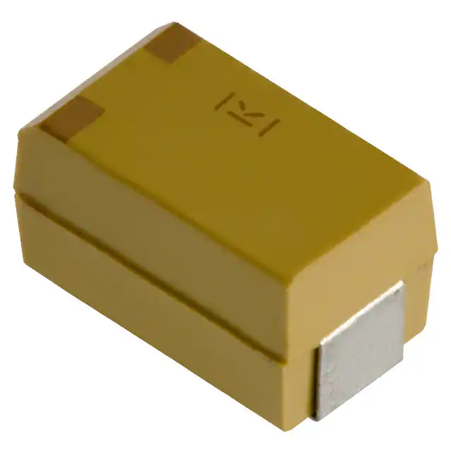
Tantalum Surface Mount Capacitors – Low ESR
T510 Multiple Anode MnO2
Overview
The low ESR, surge-robust T510 is designed for demanding
applications that require high surge current and high ripple
current capability. This series builds upon the proven
capabilities of our industrial grade tantalum chip capacitors
to offer several advantages such as low ESR, high ripple
current capability, excellent capacitance stability, and
improved resistance to high in-rush currents. These benefits
are achieved though the utilization of multiple anodes as
well as high-stress, low impedance electrical conditioning
performed prior to screening. This series is classified
as MSL (Moisture Sensitivity Level) 1 under J STD 020:
unlimited floor life time at ≤ 30°C/85% RH.
Benefits
• Meets or exceeds EIA Standard 535BAAC
• Taped and reeled per EIA 481
• High surge current capability
• Optional gold-plated terminations
• High ripple current capability
• 100% surge current test
• 100% steady-state accelerated aging
• Case sizes E and X
• ESR as low as 10 mΩ
Click image above for interactive 3D content
Open PDF in Adobe Reader for full functionality
Applications
Typical applications include decoupling and filtering in many end applications, such as DC/DC converters, portable
electronics, telecommunications, and control units requiring high ripple current capability.
Environmental Compliance
RoHS compliant (6/6) according to Directive 2002/95/EC when ordered with 100% Sn solder or gold-plated.
• Halogen-free
• Epoxy compliant with UL94 V–0
• Molded Epoxy complies for outgassing testing under ASTM E 595.
Built Into Tomorrow
© KEMET Electronics Corporation • KEMET Tower • One East Broward Boulevard
Fort Lauderdale, FL 33301 USA • 954-766-2800 • www.kemet.com
T2014_T510 • 1/7/2021
1
�Tantalum Surface Mount Capacitors – Low ESR
T510 Multiple Anode MnO2
K-SIM
For a detailed analysis of specific part numbers, please visit ksim.kemet.com to access KEMET’s K-SIM software. KEMET
K-SIM is designed to simulate behavior of components with respect to frequency, ambient temperature, and DC bias levels.
Ordering Information
T
510
X
477
M
006
A
T
E800
Capacitor
Class
Series
Case
Size
Capacitance
Code (pF)
Capacitance
Tolerance
Rated
Voltage
(VDC)
Failure Rate/
Design
Termination Finish
ESR
E
X
First two digits
represent
significant
figures. Third digit
specifies number
of zeros.
K = ±10%
M = ±20%
T=
Tantalum
Multiple
Anode
Low ESR
004 = 4
006 = 6.3
010 = 10
016 = 16
020 = 20
025 = 25
035 = 35
050 = 50
A = N/A
Z = N/A
Packaging
(C-Spec)
T = 100% Matte Tin
Last three
Blank = 7" Reel
(Sn) Plated
digits specify 7280 = 13" Reel
H = Standard Solder
ESR in mΩ.
Coated
(800 = 800
(SnPb 5% Pb minimum)
mΩ)
G = Gold Plated
(A, B, C, D, X only)
Performance Characteristics
Item
Performance Characteristics
Operating Temperature
Rated Capacitance Range
Capacitance Tolerance
Rated Voltage Range
−55°C to 125°C
10 – 1,000 µF at 120 Hz/25°C
K Tolerance (10%), M Tolerance (20%)
4 – 50 V
DF (120 Hz)
Refer to Part Number Electrical Specification Table
ESR (100 kHz)
Refer to Part Number Electrical Specification Table
Leakage Current
≤ 0.01 CV (µA) at rated voltage after 5 minutes
© KEMET Electronics Corporation • KEMET Tower • One East Broward Boulevard
Fort Lauderdale, FL 33301 USA • 954-766-2800 • www.kemet.com
T2014_T510 • 1/7/2021
2
�Tantalum Surface Mount Capacitors – Low ESR
T510 Multiple Anode MnO2
Qualification
Test
Condition
Characteristics
ΔC/C
Endurance
Storage Life
Thermal Shock
Temperature Stability
85°C at rated voltage, 2,000 hours
125°C at 2/3 rated voltage, 2,000 hours
125°C @ 0 volts, 2,000 hours
MIL–STD–202, Method 107, Condition B, mounted,
−55C° to 125° C, 1,000 cycles
Extreme temperature exposure at a
succession of continuous steps at +25°C,
−55°C, +25°C, +85°C, +125°C, +25°C
Within initial limits
DCL
Within 1.25 x initial limit
ESR
Within initial limits
ΔC/C
Within ±10% of initial value
DF
Within initial limits
DCL
Within 1.25 x initial limit
ESR
Within initial limits
ΔC/C
Within ±5% of initial value
DF
Within initial limits
DCL
Within 1.25 x initial limit
ESR
Within initial limits
+25°C
−55°C
+85°C
+125°C
ΔC/C
IL*
±10%
±10%
±20%
DF
IL
IL
1.5 x IL
1.5 x IL
DCL
IL
n/a
10 x IL
12 x IL
ΔC/C
Surge Voltage
Mechanical Shock/
Vibration
Within ±10% of initial value
DF
85°C, 1.32 x rated voltage 1,000 cycles
(125°C, 1.2 x rated voltage)
MIL–STD–202, Method 213, Condition I, 100 G peak
MIL–STD–202, Method 204, Condition D, 10 Hz to
2,000 Hz, 20 G peak
Within ±5% of initial value
DF
Within initial limits
DCL
Within initial limits
ESR
Within initial limits
ΔC/C
Within ±10% of initial value
DF
Within initial limits
DCL
Within initial limits
*IL = Initial limit
© KEMET Electronics Corporation • KEMET Tower • One East Broward Boulevard
Fort Lauderdale, FL 33301 USA • 954-766-2800 • www.kemet.com
T2014_T510 • 1/7/2021
3
�Tantalum Surface Mount Capacitors – Low ESR
T510 Multiple Anode MnO2
Electrical Characteristics
Capacitance vs. Frequency
Impedance, ESR vs. Frequency
100
100
T510X226M035ATE100_IMP
T510E476M035ATE050_IMP
T510X226M035ATE100_ESR
Capacitance (μF)
Impedance, ESR (Ohms)
T510X336M035ATE065_IMP
10
T510X336M035ATE065_ESR
T510E476M035ATE050_ESR
1
10
T510X226M035ATE100
T510X336M035ATE065
0.1
T510E476M035ATE050
0.01
100
1,000
10,000
100,000
Frequency (Hz)
1,000,000
1
10,000,000
100
1,000
10,000
100,000
1,000,000
Frequency (Hz)
10,000,000
Dimensions – Millimeters (Inches)
Metric will govern
CATHODE (-) END VIEW
SIDE VIEW
ANODE (+) END VIEW
BOTTOM VIEW
A
B
W
B
H
X
T
S
G
S
Termination cutout
at KEMET's option,
either end
Case Size
KEMET
EIA
X
7343–43
E
F
E
P
R
L
Total
Weight
Component
L
W
H
7.3 ±0.3
4.3 ±0.3
4.0 ±0.3
(0.287 ±0.012) (0.169 ±0.012) (0.157 ±0.012)
7.3 ±0.3
6.0 ±0.3
3.6 ±0.2
7360–38
(0.287 ±0.012) (0.236 ±0.012) (0.142 ±0.008)
F ±0.1 S ±0.3 B ±0.15
±(.004) ±(.012) (Ref) ±.006
2.4
(0.094)
4.1
(0.161)
1.3
(0.051)
1.3
(0.051)
0.5
(0.020)
0.5
(0.020)
X
(Ref)
P
R
T
A
G
E
(Ref) (Ref) (Ref) (Min) (Ref) (Ref)
0.10 ±0.10
1.7
1.0
0.13
3.8
3.5
3.5
(0.004 ±0.004) (0.067) (0.039) (0.005) (0.150) (0.138) (0.138)
0.10±0.10
0.13
3.8
3.5
3.5
n/a
n/a
(0.004±0.004)
(0.005) (0.150) (0.138) (0.138)
(mg)
430.15
500.73
Notes: (Ref) – Dimensions provided for reference only. For low profile cases, no dimensions are provided for B, P or R because these cases do not have a bevel or
a notch.
These weights are provided as reference. If exact weights are needed, please contact your KEMET Sales Representative
© KEMET Electronics Corporation • KEMET Tower • One East Broward Boulevard
Fort Lauderdale, FL 33301 USA • 954-766-2800 • www.kemet.com
T2014_T510 • 1/7/2021
4
�Tantalum Surface Mount Capacitors – Low ESR
T510 Multiple Anode MnO2
Table 1 – Ratings & Part Number Reference
Rated Rated
Voltage Cap
Case
Code/
Case
Size
KEMET Part
Number
DC
Leakage
VDC at 85°C
µF
KEMET/EIA
(See below for
part options)
µA at +25°C
Max/5 Min
4
4
4
4
4
4
4
6.3
6.3
6.3
6.3
6.3
10
16
16
16
16
20
20
20
20
20
20
25
25
35
35
35
35
35
35
35
35
50
50
50
50
680
1000
1000
1000
1000
1000
1000
470
680
680
680
680
330
150
150
220
220
68
68
100
100
100
100
68
100
22
22
22
33
33
47
47
47
10
10
22
22
X/7343-43
X/7343-43
X/7343-43
X/7343-43
X/7343-43
E/7360-38
E/7360-38
X/7343-43
X/7343-43
X/7343-43
E/7360-38
E/7360-38
X/7343-43
X/7343-43
X/7343-43
X/7343-43
X/7343-43
X/7343-43
X/7343-43
X/7343-43
X/7343-43
X/7343-43
X/7343-43
X/7343-43
E/7360-38
X/7343-43
X/7343-43
X/7343-43
X/7343-43
X/7343-43
X/7343-43
X/7343-43
E/7360-38
X/7343-43
X/7343-43
X/7343-43
X/7343-43
T510X687(1)004A(2)E030
T510X108(1)004A(2)E018
T510X108(1)004A(2)E023
T510X108(1)004A(2)E030
T510X108(1)004A(2)E035
T510E108(1)004A(2)E018
T510E108(1)004A(2)E010
T510X477(1)006A(2)E030
T510X687(1)006A(2)E023
T510X687(1)006A(2)E045
T510E687(1)006A(2)E023
T510E687(1)006A(2)E012
T510X337(1)010A(2)E035
T510X157(1)016A(2)E030
T510X157(1)016A(2)E040
T510X227(1)016A(2)E040
T510X227(1)016A(2)E025
T510X686(1)020A(2)E055
T510X686(1)020A(2)E045
T510X107(1)020A(2)E035
T510X107(1)020A(2)E040
T510X107(1)020A(2)E045
T510X107(1)020A(2)E055
T510X686(1)025A(2)E045
T510E107(1)025A(2)E050
T510X226(1)035A(2)E100
T510X226(1)035A(2)E080
T510X226(1)035A(2)E060
T510X336(1)035A(2)E065
T510X336(1)035A(2)E050
T510X476(1)035A(2)E055
T510X476(1)035A(2)E065
T510E476(1)035A(2)E050
T510X106(1)050A(2)E120
T510X106(1)050A(2)E090
T510X226(1)050A(2)E100
T510X226(1)050A(2)E075
27.2
40.0
40.0
40.0
40.0
40.0
40.0
29.6
42.8
42.8
42.8
42.8
33.0
24.0
24.0
35.2
35.2
14.0
14.0
20.0
20.0
20.0
20.0
17.0
25.0
7.7
7.7
7.7
11.6
11.6
16.5
16.5
16.5
5.0
5.0
11.0
11.0
VDC at 85°C
µF
KEMET/EIA
(See below for
part options)
µA at +25°C
Max/5 Min
Rated
Voltage
Rated
Cap
Case Code/
Case Size
KEMET Part Number
DC
Leakage
DF
% at +25°C
120 Hz
Max
6.0
6.0
6.0
6.0
6.0
6.0
6.0
6.0
6.0
12.0
6.0
6.0
6.0
6.0
6.0
10.0
10.0
6.0
6.0
8.0
6.0
6.0
6.0
8.0
8.0
6.0
6.0
6.0
6.0
6.0
8.0
8.0
8.0
8.0
8.0
8.0
8.0
% at +25°C
120 Hz
Max
DF
ESR
Maximum
Operating MSL
Temp
Maximum Allowable
Ripple Current (rms)
mΩ at 25°C mA at +25°C mA at +85°C mA at +125°C
100 kHz
100 kHz
100 kHz
100 kHz
Max
30
3000
2700
1200
18
3873
3486
1549
23
3426
3083
1370
30
3000
2700
1200
35
2777
2499
1111
18
3979
3581
1592
10
5339
4805
2136
30
3000
2700
1200
23
3426
3083
1370
45
2449
2204
980
23
3520
3168
1408
12
4873
4386
1949
35
2777
2499
1111
30
3000
2700
1200
40
2598
2338
1039
40
2598
2338
1039
25
3286
2957
1314
55
2216
1994
886
45
2449
2204
980
35
2777
2499
1111
40
2598
2338
1039
45
2449
2204
980
55
2216
1994
886
45
2449
2204
980
50
2387
2148
955
100
1643
1479
657
80
1837
1653
735
60
2121
1909
848
65
2038
1834
815
50
2324
2092
930
55
2216
1994
886
65
2038
1834
815
50
2387
2148
955
1500
1350
600
120
90
1732
1559
693
100
1643
1479
657
75
1897
1707
759
mΩ at 25°C mA at +25°C mA at +85°C mA at +125°C
100 kHz
100 kHz
100 kHz
100 kHz
Max
ESR
Maximum Allowable
Ripple Current (rms)
°C
125
125
125
125
125
125
125
125
125
125
125
125
125
125
125
125
125
125
125
125
125
125
125
125
125
125
125
125
125
125
125
125
125
125
125
125
125
°C
Maximum
Operating
Temp
Reflow
Temp
≤ 260°C
1
1
1
1
1
1
1
1
1
1
1
1
1
1
1
1
1
1
1
1
1
1
1
1
1
1
1
1
1
1
1
1
1
1
1
1
1
Reflow
Temp
≤ 260°C
MSL
(1) To complete KEMET part number, insert M for ±20% or K for ±10%. Designates Capacitance tolerance.
(2) To complete KEMET part number, insert T = 100% Matte Tin (Sn) Plated, G = Gold Plated, H = Standard Solder coated (SnPb 5% Pb minimum).
Designates Termination Finish.
Refer to Ordering Information for additional detail.
Higher voltage ratings and tighter tolerance product including ESR may be substituted within the same size at KEMET's option. Voltage substitution will
be marked with the higher voltage rating. Substitutions can include better than series.
© KEMET Electronics Corporation • KEMET Tower • One East Broward Boulevard
Fort Lauderdale, FL 33301 USA • 954-766-2800 • www.kemet.com
T2014_T510 • 1/7/2021
5
�Tantalum Surface Mount Capacitors – Low ESR
T510 Multiple Anode MnO2
Recommended Voltage Derating Guidelines
85°C to 125°C
120%
VR
67% of VR
100%
50% of VR
33% of VR
% Working Voltage
% Change in Working DC
Voltage with Temperature
Recommended Maximum
Application Voltage
−55°C to 85°C
80%
% Change in Working DC Voltage
with Temperature
67%
60%
40%
20%
0%
−55
Recommended Maximum
Application Voltage
(As % of Rated Voltage)
25
33%
85
Temperature (ºC)
125
Ripple Current/Ripple Voltage
Permissible AC ripple voltage and current are related to
equivalent series resistance (ESR) and the power dissipation
capabilities of the device. Permissible AC ripple voltage
which may be applied is limited by two criteria:
1. The positive peak AC voltage plus the DC bias voltage,
if any, must not exceed the DC voltage rating of the
capacitor.
2. The negative peak AC voltage in combination with
bias voltage, if any, must not exceed the allowable limits
specified for reverse voltage. See the Reverse Voltage
section for allowable limits.
The maximum power dissipation by case size can be
determined using the table at right. The maximum power
dissipation rating stated in the table must be reduced with
increasing environmental operating temperatures. Refer to
the table below for temperature compensation requirements.
Temperature Compensation Multipliers
for Maximum Ripple Current
T ≤ 25°C
1.00
T ≤ 85°C
0.90
T ≤ 125°C
0.40
T = Environmental Temperature
The maximum power dissipation rating must be reduced with increasing
environmental operating temperatures. Refer to the Temperature
Compensation Multiplier table for details.
KEMET
Case Code
EIA
Case Code
Maximum Power
Dissipation (P max)
mWatts @ 25°C
w/+20°C Rise
A
B
C
D
X
E
S
T
U
V
T510X
T510E
3216–18
3528–21
6032–28
7343–31
7343–43
7360–38
3216–12
3528–12
6032–15
7343–20
7343–43
7360–38
75
85
110
150
165
200
60
70
90
125
270
285
Using the P max of the device, the maximum allowable rms
ripple current or voltage may be determined.
I(max) = √P max/R
E(max) = Z √P max/R
I = rms ripple current (amperes)
E = rms ripple voltage (volts)
P max = maximum power dissipation (watts)
R = ESR at specified frequency (ohms)
Z = Impedance at specified frequency (ohms)
© KEMET Electronics Corporation • KEMET Tower • One East Broward Boulevard
Fort Lauderdale, FL 33301 USA • 954-766-2800 • www.kemet.com
T2014_T510 • 1/7/2021
6
�Tantalum Surface Mount Capacitors – Low ESR
T510 Multiple Anode MnO2
Reverse Voltage
Solid tantalum capacitors are polar devices and may be permanently damaged or destroyed if connected with the wrong
polarity. The positive terminal is identified on the capacitor body by a stripe plus in some cases a beveled edge. A small
degree of transient reverse voltage is permissible for short periods per the table. The capacitors should not be operated
continuously in reverse mode, even within these limits.
Temperature
Permissible Transient Reverse Voltage
25°C
85°C
125°C
15% of Rated Voltage
5% of Rated Voltage
1% of Rated Voltage
Table 2 – Land Dimensions/Courtyard
KEMET
Metric
Size
Code
Density Level A:
Maximum (Most) Land
Protrusion (mm)
Density Level B:
Median (Nominal) Land
Protrusion (mm)
Density Level C:
Minimum (Least) Land
Protrusion (mm)
Case
EIA
W
L
S
V1
V2
W
L
S
V1
V2
W
L
S
V1
V2
E
1
7360–38
4.25
2.77
3.67
10.22
7.30
4.13
2.37
3.87
9.12
6.80
4.03
1.99
4.03
8.26
6.54
X1
7343–43
2.55
2.77
3.67
10.22
5.60
2.43
2.37
3.87
9.12
5.10
2.33
1.99
4.03
8.26
4.84
Density Level A: For low-density product applications. Recommended for wave solder applications and provides a wider process window for reflow
solder processes.
Density Level B: For products with a moderate level of component density. Provides a robust solder attachment condition for reflow solder processes.
Density Level C: For high component density product applications. Before adapting the minimum land pattern variations the user should perform
qualification testing based on the conditions outlined in IPC standard 7351 (IPC–7351).
1
Height of these chips may create problems in wave soldering.
2
Land pattern geometry is too small for silkscreen outline.
V1
L
L
W
W
V2
S
Grid Placement Courtyard
© KEMET Electronics Corporation • KEMET Tower • One East Broward Boulevard
Fort Lauderdale, FL 33301 USA • 954-766-2800 • www.kemet.com
T2014_T510 • 1/7/2021
7
�Tantalum Surface Mount Capacitors – Low ESR
T510 Multiple Anode MnO2
Soldering Process
Please note that although the X/7343–43 case size can
withstand wave soldering, the tall profile (4.3 mm maximum)
dictates care in wave process development.
Hand soldering should be performed with care due to the
difficulty in process control. If performed, care should be
taken to avoid contact of the soldering iron to the molded
case. The iron should be used to heat the solder pad,
applying solder between the pad and the termination, until
reflow occurs. Once reflow occurs, the iron should be
removed immediately. “Wiping” the edges of a chip and
heating the top surface is not recommended.
During typical reflow operations, a slight darkening of the
gold-colored epoxy may be observed. This slight darkening is
normal and not harmful to the product. Marking permanency
is not affected by this change.
Profile Feature
SnPb Assembly Pb-Free Assembly
Preheat/Soak
Temperature Minimum (TSmin)
100°C
150°C
Temperature Maximum (TSmax)
150°C
200°C
Time (ts) from Tsmin to Tsmax)
60 – 120 seconds
60 – 120 seconds
Ramp-up Rate (TL to TP)
3°C/second maximum
3°C/second maximum
Liquidous Temperature (TL)
183°C
217°C
Time Above Liquidous (tL)
60 – 150 seconds
220°C*
235°C**
60 – 150 seconds
250°C*
260°C**
20 seconds maximum
30 seconds maximum
6°C/second maximum
6°C/second maximum
6 minutes maximum
8 minutes maximum
Peak Temperature (TP)
Time within 5°C of Maximum
Peak Temperature (tP)
Ramp-down Rate (TP to TL)
Time 25°C to Peak
Temperature
Note: All temperatures refer to the center of the package, measured on the
package body surface that is facing up during assembly reflow.
* For Case Size height > 2.5 mm
** For Case Size height ≤ 2.5 mm
TP
TL
Temperature
KEMET’s families of surface mount capacitors are
compatible with wave (single or dual), convection, IR,
or vapor phase reflow techniques. Preheating of these
components is recommended to avoid extreme thermal
stress. KEMET's recommended profile conditions for
convection and IR reflow reflect the profile conditions of the
IPC/J–STD–020D standard for moisture sensitivity testing.
The devices can safely withstand a maximum of three reflow
passes at these conditions.
tP
Maximum Ramp-up Rate = 3°C/second
Maximum Ramp-down Rate = 6°C/second
tL
Tsmax
Tsmin
25
ts
25°C to Peak
Time
Storage
Tantalum chip capacitors should be stored in normal working environments. While the chips themselves are quite robust in
other environments, solderability will be degraded by exposure to high temperatures, high humidity, corrosive atmospheres,
and long term storage. In addition, packaging materials will be degraded by high temperature – reels may soften or warp
and tape peel force may increase. KEMET recommends that maximum storage temperature not exceed 40°C and maximum
storage humidity not exceed 60% relative humidity. Temperature fluctuations should be minimized to avoid condensation
on the parts and atmospheres should be free of chlorine and sulphur bearing compounds. For optimized solderability chip
stock should be used promptly, preferably within three years of receipt.
© KEMET Electronics Corporation • KEMET Tower • One East Broward Boulevard
Fort Lauderdale, FL 33301 USA • 954-766-2800 • www.kemet.com
T2014_T510 • 1/7/2021
8
�Tantalum Surface Mount Capacitors – Low ESR
T510 Multiple Anode MnO2
Construction
Polarity Stripe (+)
Molded Epoxy
Case
Detailed Cross Section
Silver Paint
(Fourth Layer)
Polarity
Bevel (+)
Leadframe
(− Cathode)
Washer
Tantalum Wire
Tantalum Wire
Weld
(to attach wire)
Carbon
(Third Layer)
Washer
Silver Adhesive
Leadframe
(+ Anode)
Molded Epoxy
Case
MnO2
(Second Layer)
Ta2O5 Dielectric
(First Layer)
Tantalum
Capacitor Marking
Date Code *
1 digit = last number of year
6 = 2016
7 = 2017
8 = 2018
9 = 2019
0 = 2020
2nd and 3rd digit = week of the
year
01 = 1st week of the year to
52 = 52nd week of the year
st
KEMET
Multi-Anode
MnO2
Polarity
Indicator (+)
Picofarad
Code
KEMET
ID
Rated
Voltage
Date
Code*
* 036 = 36th week of 2020
© KEMET Electronics Corporation • KEMET Tower • One East Broward Boulevard
Fort Lauderdale, FL 33301 USA • 954-766-2800 • www.kemet.com
T2014_T510 • 1/7/2021
9
�Tantalum Surface Mount Capacitors – Low ESR
T510 Multiple Anode MnO2
Tape & Reel Packaging Information
KEMET’s molded chip capacitor families are packaged in 8 and 12 mm plastic tape on 7" and 13" reels in accordance with
EIA Standard 481: Embossed Carrier Taping of Surface Mount Components for Automatic Handling. This packaging system
is compatible with all tape-fed automatic pick-and-place systems.
Right hand
orientation
only
(+)
Embossed carrier
(−)
Embossment
Top tape thickness
0.10 mm (0.004”)
maximum thickness
180 mm (7.0”) or
330 mm (13.”)
8 mm (0.315”) or
12 mm (0.472”)
Table 3 – Packaging Quantity
Case Code
KEMET
S
T
M
U
L
W
Z
V
A
B
C
D
Q
Y
X
E/T428P
H
O
EIA
3216-12
3528-12
3528-15
6032-15
6032-19
7343-15
7343-17
7343-20
3216-18
3528-21
6032-28
7343-31
7343-12
7343-40
7343-43
7360-38
7360-20
7360-43
Tape Width
(mm)
7" Reel*
13" Reel*
8
8
8
12
12
12
12
12
8
8
12
12
12
12
12
12
12
12
2,500
3,000
2,500
1,000
1,000
1,000
1,000
1,000
2,000
2,000
500
500
1,000
500
500
500
1,000
250
10,000
10,000
8,000
5,000
3,000
3,000
3,000
3,000
9,000
8,000
3,000
2,500
3,000
2,000
2,000
2,000
2,500
1,000
* No C-Spec required for 7" reel packaging. C-7280 required for 13" reel packaging.
© KEMET Electronics Corporation • KEMET Tower • One East Broward Boulevard
Fort Lauderdale, FL 33301 USA • 954-766-2800 • www.kemet.com
T2014_T510 • 1/7/2021
10
�Tantalum Surface Mount Capacitors – Low ESR
T510 Multiple Anode MnO2
Figure 1 – Embossed (Plastic) Carrier Tape Dimensions
P2
T
T2
ØD0
P0
(10 pitches cumulative
tolerance on tape ±0.2 mm)
A0
E1
F
K0
B1
E2
B0
S1
W
P1
T1
Center Lines of Cavity
B1 is for tape feeder reference only,
including draft concentric about B0.
Embossment
For cavity size,
see Note 1, Table 4
ØD1
Cover Tape
User Direction of Unreeling
Table 4 – Embossed (Plastic) Carrier Tape Dimensions
Metric will govern
Constant Dimensions — Millimeters (Inches)
Tape Size
8 mm
12 mm
D1 Minimum
Note 1
D0
1.5 +0.10/−0.0
(0.059 +0.004/−0.0)
1.0
(0.039)
1.5
(0.059)
E1
P0
R Reference S1 Minimum
T1
T Maximum
Note 2
Note 3
Maximum
P2
1.75 ±0.10
4.0 ±0.10
2.0 ±0.05
(0.069 ±0.004) (0.157 ±0.004) (0.079 ±0.002)
25.0
(0.984)
30
(1.181)
0.600
(0.024)
0.600
(0.024)
0.100
(0.004)
Variable Dimensions — Millimeters (Inches)
Tape Size
Pitch
B1 Maximum
Note 4
8 mm
Single (4 mm)
4.35
(0.171)
6.25
(0.246)
12 mm
Single (4 mm)
and Double
(8 mm)
8.2
(0.323)
10.25
(0.404)
E2 Minimum
F
P1
3.5 ±0.05
2.0 ±0.05 or 4.0 ±0.10
(0.138 ±0.002) (0.079 ±0.002 or 0.157 ±0.004)
2.0 ±0.05 (0.079 ±0.002) or
5.5 ±0.05
4.0 ±0.10 (0.157 ±0.004) or
(0.217 ±0.002)
8.0 ±0.10 (0.315 ±0.004)
T2 Maximum W Maximum A0, B0 & K0
2.5
(0.098)
8.3
(0.327)
4.6
(0.181)
12.3
(0.484)
Note 5
1. The embossment hole location shall be measured from the sprocket hole controlling the location of the embossment. Dimensions of embossment
location and hole location shall be applied independent of each other.
2. The tape, with or without components, shall pass around R without damage (see Figure 4).
3. If S1 < 1.0 mm, there may not be enough area for cover tape to be properly applied (see EIA Standard 481–D, paragraph 4.3, section b).
4. B1 dimension is a reference dimension for tape feeder clearance only.
5. The cavity defined by A0, B0 and K0 shall surround the component with sufficient clearance that:
(a) the component does not protrude above the top surface of the carrier tape.
(b) the component can be removed from the cavity in a vertical direction without mechanical restriction, after the top cover tape has been removed.
(c) rotation of the component is limited to 20° maximum for 8 and 12 mm tapes (see Figure 2).
(d) lateral movement of the component is restricted to 0.5 mm maximum for 8 mm and 12 mm wide tape (see Figure 3).
(e) see Addendum in EIA Standard 481–D for standards relating to more precise taping requirements.
© KEMET Electronics Corporation • KEMET Tower • One East Broward Boulevard
Fort Lauderdale, FL 33301 USA • 954-766-2800 • www.kemet.com
T2014_T510 • 1/7/2021
11
�Tantalum Surface Mount Capacitors – Low ESR
T510 Multiple Anode MnO2
Packaging Information Performance Notes
1. Cover tape break force: 1.0 kg minimum.
2. Cover tape peel strength: The total peel strength of the cover tape from the carrier tape shall be:
Tape Width
Peel Strength
8 mm
0.1 to 1.0 newton (10 to 100 gf)
12 mm
0.1 to 1.3 newton (10 to 130 gf)
The direction of the pull shall be opposite the direction of the carrier tape travel. The pull angle of the carrier tape shall be
165° to 180° from the plane of the carrier tape. During peeling, the carrier and/or cover tape shall be pulled at a velocity of
300 ±10 mm/minute.
3. Labeling: Bar code labeling (standard or custom) shall be on the side of the reel opposite the sprocket holes. Refer to EIA
Standards 556 and 624.
Figure 2 – Maximum Component Rotation
°
T
Maximum Component Rotation
Top View
Maximum Component Rotation
Side View
Typical Pocket Centerline
Tape
Width (mm)
8, 12
Bo
Maximum
Rotation (
20
°
T)
°
s
Tape
Maximum
Width (mm) Rotation (
8, 12
20
Typical Component Centerline
°
S)
Ao
Figure 3 – Maximum Lateral Movement
Figure 4 – Bending Radius
8 and 12 mm Tape
0.5 mm maximum
0.5 mm maximum
Embossed
Carrier
Punched
Carrier
R
© KEMET Electronics Corporation • KEMET Tower • One East Broward Boulevard
Fort Lauderdale, FL 33301 USA • 954-766-2800 • www.kemet.com
Bending
Radius
R
T2014_T510 • 1/7/2021
12
�Tantalum Surface Mount Capacitors – Low ESR
T510 Multiple Anode MnO2
Figure 5 – Reel Dimensions
Full Radius,
See Note
W3
(Includes
flange distortion
at outer edge)
Access Hole at
Slot Location
(Ø 40 mm minimum)
W2
D
A
(See Note)
N
C
(Arbor hole
diameter)
B
(see Note)
(Measured at hub)
W1
(Measured at hub)
If present,
tape slot in core
for tape start:
2.5 mm minimum width x
10.0 mm minimum depth
Note: Drive spokes optional; if used, dimensions B and D shall apply.
Table 5 – Reel Dimensions
Metric will govern
Constant Dimensions — Millimeters (Inches)
Tape Size
A
B Minimum
C
D Minimum
8 mm
178 ±0.20
(7.008 ±0.008)
or
330 ±0.20
(13.000 ±0.008)
1.5
(0.059)
13.0 +0.5/−0.2
(0.521 +0.02/−0.008)
20.2
(0.795)
12 mm
Variable Dimensions — Millimeters (Inches)
Tape Size
8 mm
12 mm
N Minimum
W1
W2 Maximum
W3
50
(1.969)
8.4 +1.5/−0.0
(0.331 +0.059/−0.0)
12.4 +2.0/−0.0
(0.488 +0.078/−0.0)
14.4
(0.567)
18.4
(0.724)
Shall accommodate tape
width without interference
© KEMET Electronics Corporation • KEMET Tower • One East Broward Boulevard
Fort Lauderdale, FL 33301 USA • 954-766-2800 • www.kemet.com
T2014_T510 • 1/7/2021
13
�Tantalum Surface Mount Capacitors – Low ESR
T510 Multiple Anode MnO2
Figure 6 – Tape Leader & Trailer Dimensions
Embossed Carrier
Carrier Tape
Punched Carrier
8 and 12 mm only
END
Round Sprocket Holes
START
Top Cover Tape
Elongated Sprocket Holes
(32 mm tape and wider)
Trailer
160 mm minimum
Components
100 mm
minimum Leader
400 mm minimum
Top Cover Tape
Figure 7 – Maximum Camber
Elongated Sprocket Holes
(32 mm and wider tapes)
Carrier Tape
Round Sprocket Holes
1 mm maximum, either direction
Straight Edge
250 mm
© KEMET Electronics Corporation • KEMET Tower • One East Broward Boulevard
Fort Lauderdale, FL 33301 USA • 954-766-2800 • www.kemet.com
T2014_T510 • 1/7/2021
14
�Tantalum Surface Mount Capacitors – Low ESR
T510 Multiple Anode MnO2
KEMET Electronics Corporation Sales Offices
For a complete list of our global sales offi ces, please visit www.kemet.com/sales.
Disclaimer
All product specifi cations, statements, information and data (collectively, the “Information”) in this datasheet are subject to change. The customer is responsible for
checking and verifying the extent to which the Information contained in this publication is applicable to an order at the time the order is placed. All Information given
herein is believed to be accurate and reliable, but it is presented without guarantee, warranty, or responsibility of any kind, expressed or implied.
Statements of suitability for certain applications are based on KEMET Electronics Corporation’s (“KEMET”) knowledge of typical operating conditions for such
applications, but are not intended to constitute – and KEMET specifi cally disclaims – any warranty concerning suitability for a specifi c customer application or use.
The Information is intended for use only by customers who have the requisite experience and capability to determine the correct products for their application. Any
technical advice inferred from this Information or otherwise provided by KEMET with reference to the use of KEMET’s products is given gratis, and KEMET assumes
no obligation or liability for the advice given or results obtained.
Although KEMET designs and manufactures its products to the most stringent quality and safety standards, given the current state of the art, isolated component
failures may still occur. Accordingly, customer applications which require a high degree of reliability or safety should employ suitable designs or other safeguards
(such as installation of protective circuitry or redundancies) in order to ensure that the failure of an electrical component does not result in a risk of personal injury
or property damage.
Although all product–related warnings, cautions and notes must be observed, the customer should not assume that all safety measures are indicted or that other
measures may not be required.
KEMET is a registered trademark of KEMET Electronics Corporation.
© KEMET Electronics Corporation • KEMET Tower • One East Broward Boulevard
Fort Lauderdale, FL 33301 USA • 954-766-2800 • www.kemet.com
T2014_T510 • 1/7/2021
15
�


 工商网监
湘ICP备2023018690号
工商网监
湘ICP备2023018690号
