UHF MAGICSTRAP® Data Sheet
LXMS21ACMF-183
1. General descriptions
Murata MAGICSTRAP® is an innovative RFID module
designed to operate in electronic products/applications.
It incorporates an industry standard IC.
[Features]
・ Compliant with ISO18000-63 and EPC Global Gen2v2
・ Reflow SMT compatible
・ Ultra small package (2.0 x 1.2 x 0.5)
・ RoHS compliant
2. Part number / IC / Memory
P/N
IC
TID
EPC
LXMS21ACMF–183
Impinj MonzaR6
96bits
96bit
3. Block diagram
Fig. 1 shows MAGICSTRAP® block diagram.
Analog F/E
Controller
TID Memory
Integrated Circuit
Fig. 1 MAGICSTRAP®Block Diagram
All Rights Reserved, Copyright© Murata Manufacturing Co., Ltd.
Tentative/Confidential
1
V1.0 January 2016
�UHF MAGICSTRAP® Data Sheet
LXMS21ACMF-183
4. Mechanical information
4-1. Dimensions
T
L
W
[mm]
T
b
a
c2
c1
d
®
Fig. 2 MAGICSTRAP
d
Package Dimension
4-2. Recommended land pattern
Mark
Size
f
0.90
g
1.00
h
0.40
[mm]
Fig. 3 Land Pattern
All Rights Reserved, Copyright© Murata Manufacturing Co., Ltd.
Tentative/Confidential
2
V1.0 January 2016
�UHF MAGICSTRAP® Data Sheet
LXMS21ACMF-183
5. Electrical performance
5-1. Frequency range
865 – 928MHz
6. Absolute rating
Storage Temperature: -40oC ~ +85oC
Operating Temperature: -40oC ~ +85oC
MSL Rating: MSL1
ESD: 2kV (Human Body Model, JESD22-A114-B)
7. RoHS compliance
MAGICSTRAP® is compliant with RoHS directive.
All Rights Reserved, Copyright© Murata Manufacturing Co., Ltd.
Tentative/Confidential
3
V1.0 January 2016
�UHF MAGICSTRAP® Data Sheet
LXMS21ACMF-183
8. Reference antenna design on PCB
8-1. Top layer
Mounting pattern (normal)
Please conduct to PCB ground
8-2. How to design layers below the mounting pattern
Please remove all the copper pattern area from all layers of the PCB, if it is located under mounting pattern
on surface layer.
Surface Layer
Other Layers
Acceptable
Not Acceptable
All Rights Reserved, Copyright© Murata Manufacturing Co., Ltd.
Tentative/Confidential
4
V1.0 January 2016
�UHF MAGICSTRAP® Data Sheet
LXMS21ACMF-183
8-3 how to put via hole
Please put via holes as shown in the figure below. If there is no via hole in multi layered PCB, unnecessary
inductance degrade performance.
8-3-1 For normal pattern
The example of via hole layout
0.5mm(★)
2.5mm pitch
2.5mm pitch
5mm pitch
1mm(★)
2.75mm pitch
:via hole
●
5.25mm pitch
diameter:0.3mmΦ
pitch:2.5mm, 2.75mm(around pattern)
5mm, 5.25 mm(other)
At the point of (★), The less value will get the less degradation.
Also increasing the number of via holes will get PCB less degradation.
At blue arrow direction, Please place the via holes to the edge of the board.
(If there is a GND electrode on other layers)
8-3-2 For small pattern
The example of via hole layout
0.5mm(★)
2.5mm pitch
1.5mm pitch
3.75mm pitch
1mm(★)
2.75mm pitch
5.25mm pitch
:via hole
●
diameter:0.3mmΦ
pitch:1.5mm, 2.75mm(around pattern)
3.75, 5.25 mm(other)
At the point of (★), The less value will get the less degradation.
Also increasing the number of via holes will get PCB less degradation.
At blue arrow direction, Please place the via holes to the edge of the board.
(If there is a GND electrode on other layers)
All Rights Reserved, Copyright© Murata Manufacturing Co., Ltd.
Tentative/Confidential
5
V1.0 January 2016
�UHF MAGICSTRAP® Data Sheet
LXMS21ACMF-183
8-4. Reading distance
Max. 9.0meter (at 4wEIRP, with 15cm length of PCB ground)
The reading distance of MAGICSTRAP® onto PCB, depends on the length of PCB ground.
8-5. Metal enclosure under printed circuit board:
When the PCB is in close proximity to the metal enclosure, sensitivity is reduced. Removing material
directly under the MAGICSTRAP® antenna pattern will greatly improve sensitivity.
All Rights Reserved, Copyright© Murata Manufacturing Co., Ltd.
Tentative/Confidential
6
V1.0 January 2016
�UHF MAGICSTRAP® Data Sheet
LXMS21ACMF-183
8-6. Antenna location on PCB
Important area of PCB ground is the edge part shown as “dark green” below. The mounting pattern should be
located closest to the edge of the PCB. Variations of ideal design are also acceptable.
8-7. Position of MAGICSTRAP® on PCB:
MAGICSTRAP® should be centered on the long side of the PCB to maximize read range. The following
illustrates the relationship between “X” length and read range.
Length “X” (cm) Read Range (m)
5
7
2
5
1
3.5
All Rights Reserved, Copyright© Murata Manufacturing Co., Ltd.
Tentative/Confidential
7
V1.0 January 2016
�UHF MAGICSTRAP® Data Sheet
LXMS21ACMF-183
9. Tape and Reel Packing
9-1. Dimensions of Tape (Plastic tape)
9-2. Dimensions of Reel
9±0.3
φ13.0±0.2
(φ180)
(φ60)
2.0±0.5
14.4 max
[mm]
All Rights Reserved, Copyright© Murata Manufacturing Co., Ltd.
Tentative/Confidential
8
V1.0 January 2016
�UHF MAGICSTRAP® Data Sheet
LXMS21ACMF-183
9-3. Leader and Tail tape
All Rights Reserved, Copyright© Murata Manufacturing Co., Ltd.
Tentative/Confidential
9
V1.0 January 2016
�UHF MAGICSTRAP® Data Sheet
LXMS21ACMF-183
9-4. Taping direction
The tape for chips are wound clockwise, the feeding holes to the right side as the tape is pulled toward the
user.
9-5. Quantity per reel
Packaging unit: 5,000 pcs / reel
9-6. Material
Base tape……Plastic
Reel……Plastic
Cover tape and cavity tape are made with anti-static processing.
9-7. Strength/Peeling force
Tear off strength against pulling of cover tape: 5N min.
Peel off force: 0.7N max., in the direction as shown below.
0.7 N max.
165 ~ 180 °
Cover tape
Base tape
9-8. Other packaging options
Other packaging options, such as FFC (Free Film Carrier) will be considered based upon customers’
request.
10. Contact window
URL : http://www.murata.com/en-global/products/rfid
" MAGICSTRAP® " is the registered trademark of Murata Manufacturing. Co., Ltd.
For any inquiries/queries, please feel free to contact us.
All Rights Reserved, Copyright© Murata Manufacturing Co., Ltd.
Tentative/Confidential
10
V1.0 January 2016
�
很抱歉,暂时无法提供与“LXMS21ACMF-183”相匹配的价格&库存,您可以联系我们找货
免费人工找货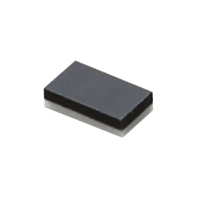


 工商网监
湘ICP备2023018690号
工商网监
湘ICP备2023018690号
