1 (47)
Data Sheet
SCL3300-D01
3-axis inclinometer with angle output
and digital SPI interface
Features
3-axis (XYZ) inclinometer
User selectable measurement modes:
3000 LSB/g with 70 Hz LPF
6000 LSB/g with 40 Hz LPF
12000 LSB/g with 10 Hz LPF
Angle output resolution 0.0055°/LSB
−40°C…+125°C operating range
3.0V…3.6V supply voltage
SPI digital interface
Ultra-low 0.001 °/√Hz noise density
Excellent offset stability
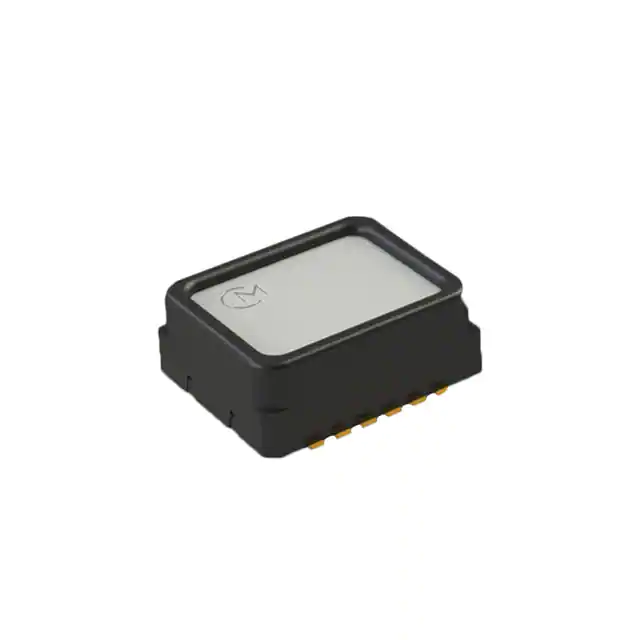
Size 8.6 x 7.6 x 3.3 mm (l × w × h)
Proven capacitive 3D-MEMS technology
Applications
SCL3300-D01 is targeted at applications demanding high
stability and accuracy with tough environmental
requirements.
Typical applications include:
Leveling
Tilt sensing
Machine control
Structural health monitoring
Inertial measurement units (IMUs)
Robotics
Positioning and guidance systems
Overview
The SCL3300-D01 is a high performance inclinometer sensor component. It is a three-axis inclinometer sensor with
angle output based on Murata's proven capacitive 3D-MEMS technology. Signal processing is done in a mixed
signal ASIC with flexible SPI digital interface. Sensor element and ASIC are packaged into 12 pin pre-molded
plastic housing that guarantees reliable operation over product's lifetime.
The SCL3300-D01 is designed, manufactured and tested for high stability, reliability and quality requirements. The
component has extremely stable output over wide range of temperature and vibration. The component has several
advanced self-diagnostics features, is suitable for SMD mounting and is compatible with RoHS and ELV directives.
Murata Electronics Oy
www.murata.com
SCL3300-D01
Doc.No. 4921
Rev. 2
�2 (47)
TABLE OF CONTENTS
1 Introduction .................................................................................................................................4
2
Specifications .............................................................................................................................4
2.1
Abbreviations .........................................................................................................................4
2.2
General Specifications ...........................................................................................................4
2.3
Performance Specifications for Inclinometer ..........................................................................5
2.4
Performance Specification for Temperature Sensor ...............................................................7
2.5
Specification for Angle Outputs ..............................................................................................7
2.6
Absolute Maximum Ratings ...................................................................................................8
2.7
AEC-Q100 Testing .................................................................................................................8
2.8
Pin Description.......................................................................................................................9
2.9
Typical performance characteristics .....................................................................................10
2.10
Digital I/O Specification ........................................................................................................13
2.10.1
SPI DC Characteristics ................................................................................................13
2.10.2
SPI AC Characteristics ................................................................................................14
2.11
Measurement Axis and Directions........................................................................................15
2.11.1
2.12
Package Characteristics ......................................................................................................17
2.12.1
2.13
3
5
PCB Footprint ......................................................................................................................18
Factory Calibration ...............................................................................................................19
Component Operation, Reset and Power Up ..........................................................................20
4.1
Component Operation..........................................................................................................20
4.2
Start-up sequence ...............................................................................................................21
4.3
Operation modes .................................................................................................................22
Component Interfacing .............................................................................................................22
5.1.1
General...........................................................................................................................22
5.1.2
Protocol ..........................................................................................................................23
5.1.3
SPI frame .......................................................................................................................24
5.1.4
Operations ......................................................................................................................25
5.1.5
Return Status..................................................................................................................26
5.2
6
Package Outline Drawing ............................................................................................17
General Product Description....................................................................................................19
3.1
4
Measurement Ranges on Inclination Modes ................................................................16
Checksum (CRC).................................................................................................................26
Register Definition ....................................................................................................................27
6.1
Sensor Data Block ...............................................................................................................29
6.1.1
Example of Acceleration Data Conversion ......................................................................30
6.1.2
Example of Temperature Data Conversion .....................................................................31
Murata Electronics Oy
www.murata.com
SCL3300-D01
Doc.No. 4921
Rev. 2
�3 (47)
6.1.3
6.2
STO .....................................................................................................................................33
6.2.1
6.3
Example of Self-Test Analysis ........................................................................................34
STATUS ..............................................................................................................................35
6.3.1
6.4
Example of Angle Data Conversion ................................................................................32
Example of STATUS summary reset ..............................................................................37
Error Flag Block ...................................................................................................................38
6.4.1 ERR_FLAG1 ........................................................................................................................38
6.4.2 ERR_FLAG2 ........................................................................................................................39
6.5
CMD ....................................................................................................................................40
6.6
ANG_CTRL .........................................................................................................................41
6.7
WHOAMI .............................................................................................................................41
6.8
Serial Block ..........................................................................................................................42
6.8.1
6.9
7
Example of Resolving Serial Number..............................................................................43
SELBANK ............................................................................................................................44
Application information ............................................................................................................44
7.1
Application Circuitry and External Component Characteristics .............................................44
7.2
Assembly Instructions ..........................................................................................................46
8
Frequently Asked Questions....................................................................................................46
9
Order Information .....................................................................................................................47
Murata Electronics Oy
www.murata.com
SCL3300-D01
Doc.No. 4921
Rev. 2
�4 (47)
1
Introduction
This document contains essential technical information about the SCL3300-D01 sensor
including specifications, SPI interface descriptions, user accessible register details,
electrical properties and application information. This document should be used as a
reference when designing in SCL3300-D01 component.
2
2.1
Specifications
Abbreviations
ASIC
SPI
RT
FS
CSB
SCK
MOSI
MISO
MCU
STO
2.2
Application Specific Integrated Circuit
Serial Peripheral Interface
Room Temperature, +23 °C
Full Scale
Chip Select
Serial Clock
Master Out Slave In
Master In Slave Out
Microcontroller
Self-test Output
General Specifications
General specifications for SCL3300-D01 component are presented in Table 1. All
analog voltages are related to the potential at AVSS and all digital voltages are related
to the potential at DVSS.
Table 1 General specifications
Parameter
Condition
Supply voltage: VDD
SPI supply voltage: DVIO
Current consumption: I_VDD
Current consumption: I_VDD in
power down mode
Murata Electronics Oy
www.murata.com
Must never be higher than VDD
Min
Nom
Max
Units
3.0
3.3
3.6
V
3.0
3.3
3.6
V
Temperature range -40 ... +125 °C
Standard operation
1.2
Mode 4
2.1
Temperature range -40 ... +125 °C
Power down mode (PD)
Typical value is at room temperature
(+23°C)
SCL3300-D01
3
Doc.No. 4921
Rev. 2
mA
10
µA
�5 (47)
2.3
Performance Specifications for Inclinometer
Table 2 Inclinometer performance specifications. Supply voltage VDD = 3.3 V and room
temperature (RT) +23 °C unless otherwise specified. Definition of gravitational acceleration:
g = 9.819 m/s2.
Parameter
Measurement range
Condition
Min
Max
Unit
Mode 1
Mode 2
Mode 3, Mode 4(A
1.2
2.4
-
g
Mode 1
Mode 2
Mode 3, Mode 4(A
±90
±90
(±10)
°
All modes, X, Z channels
-20
-1.15
20
1.15
mg
°
All modes, Y channel
-25
-1.45
20
1.15
mg
°
-40°C ... +125°C, X, Y channels
-10
-0.57
10
0.57
mg
°
-40°C ... +125°C, Z channel
-15
-0.86
15
0.86
mg
°
All modes, X, Z channels
-8
-0.46
±4
±0.23
8
0.46
mg
°
All modes, Y channels
-12
-0.69
±6
±0.34
12
0.69
mg
°
Offset error (B
Offset temperature dependency (C
Offset lifetime drift (D
Sensitivity (acceleration output)
Nom
Mode 1
Mode 2
Mode 3, Mode 4
6000
3000
12000
Mode 1
Mode 2
Mode 3, Mode 4
105
52
209
LSB/°
182
LSB/°
valid only between 0…1°
LSB/g
(E
Sensitivity (inclination output)
All modes
Sensitivity error (B
-40°C ... +125°C
Mode 1
-0.7
0.7
%
Sensitivity temperature
dependency (C
-40°C ... +125°C
Mode 1
-0.3
0.3
%
Linearity error (F
-1g ... +1g range
-4
4
mg
Integrated noise (RMS,
accelerometer) (G
Mode 3, X, Y, Z channels
Mode 4, X, Z channels
Mode 4, Y channel
0.13
0.08
0.06
mgRMS
Mode 3, X, Y, Z channels
Mode 4, X, Z channels
Mode 4, Y channel
32
20
15
µg/√Hz
Mode 3, X, Y, Z channels
Mode 4, X, Z channels
Mode 4, Y channel
0.0018
0.0012
0.0009
°/√Hz
Noise density (G
Cross axis sensitivity (H
Amplitude response,
-3dB frequency
Murata Electronics Oy
www.murata.com
per axis
-1.5
±0.2
1.5
%
Mode 1
40
Hz
Mode 2
70
Hz
Mode 3, Mode 4
10
Hz
SCL3300-D01
Doc.No. 4921
Rev. 2
�6 (47)
Parameter
Power on start-up
Condition
time(I
Min
Nom
Max
Unit
Mode 1
25
ms
Mode 2
15
ms
Mode 3, Mode 4
100
ms
2000
Hz
ODR
Min/Max values are ±3 sigma variation limits from test population at the minimum. Min/Max values are not guaranteed.
A)
Inclination mode. Dynamic range is dependent on orientation in gravity. See Chapter 2.11.1
B)
Includes calibration error, temperature, supply voltage and drift over lifetime.
C) Deviation from value at room temperature (RT).
D) Min/Max results based on the maximum ±3 sigma variation limits of the following tests:
HTOL bake (+125 °C, 1000h), TC (-50 °C / +150 °C, 1000 cycles), THB (85 °C / 85 %RH).
E)
Angle calculated using 1g * SIN(θ), where θ is the inclination angle relative to the 0g position. Due to
characteristics of sine function sensitivity is inversely proportional to inclination angle. Reported values
are valid only between 0° to ±1°.
F)
Straight line through specified measurement range end points.
G) SPI communication may affect the noise level. Used SPI clock should be carefully validated.
Recommended SPI clock is 2 MHz - 4 MHz to achieve the best performance; see section 2.10.2 SPI
AC Characteristics for details.
H) Cross axis sensitivity is the maximum sensitivity in the plane perpendicular to the measuring direction.
X-axis output cross axis sensitivity (cross axis for Y and Z-axis outputs are defined correspondingly):
I)
Cross axis for Y axis = Sensitivity Y / Sensitivity X
Cross axis for Z axis = Sensitivity Z / Sensitivity X
Power on start-up time is specified according to recommended start-up sequence; see section
4.2 Start-up sequence for details.
Murata Electronics Oy
www.murata.com
SCL3300-D01
Doc.No. 4921
Rev. 2
�7 (47)
2.4
Performance Specification for Temperature Sensor
Table 3 Temperature sensor performance specifications.
Parameter
Condition
Min.
Temperature signal range
Typ
-50
Temperature signal sensitivity
Direct 16-bit word
Temperature signal offset
°C output
Max.
Unit
+150
°C
18.9
-10
LSB/°C
10
°C
Temperature is converted to °C with following equation:
Temperature [°C] = -273 + (TEMP / 18.9),
where TEMP is temperature sensor output register content in decimal format.
2.5
Specification for Angle Outputs
Angles are formed from acceleration with following equations:
ANG_X = atan2(accx / √(accy^2 + accz^2)),
ANG_Y = atan2(accy / √(accx^2 + accz^2)),
ANG_Z = atan2(accz / √(accx^2 + accy^2)),
where accx, accy, and accz are accelerations to each direction and ANG_X, ANG_Y,
and ANG_Z are angle output register content in 16-bit binary format.
Angles are converted to degrees with following equation:
Angle [°] = d'ANG_% / 2^14 * 90,
where d'ANG_% is angle output register (ANG_X, ANG_Y, ANG_Z) content in decimal
format. See 6.1.3 Example of Angle Data Conversion for more information.
Murata Electronics Oy
www.murata.com
SCL3300-D01
Doc.No. 4921
Rev. 2
�8 (47)
2.6
Absolute Maximum Ratings
Within the maximum ratings (Table 4), no damage to the component shall occur.
Parametric values may deviate from specification, yet no functional failure shall occur.
Table 4. Absolute maximum ratings.
2.7
Symbol
Description
Min.
Max.
Unit
VDD
Supply voltage analog circuitry
-0.3
Typ
4.3
V
DIN/DOUT
Maximum voltage at digital input and output pins
-0.3
DVIO+0.3
V
Topr
Operating temperature range
-40
+125
°C
Tstg
Storage temperature range
-40
+150
°C
ESD_HBM
ESD according Human Body Model (HBM)
Q100-002
-2000
2000
ESD_CDM
ESD according Charged Device Model (CDM)
Q100-011
-1000
1000
US
Ultrasonic agitation (cleaning, welding, etc.)
V
V
Prohibited
AEC-Q100 Testing
The SCL3300 product family is tested according to AEC-Q100 Grade 1, revision H.
Deviations to the requirements are presented in Table 5.
Table 5. Deviations to AEC-Q100 requirements.
Stress
ABV
Package Drop
DROP
Requirement
Deviation
Drop part on each of 6 axes once
10 Drops, random orientation, drop
from a height of 1.2m onto a concrete
height 0.8m1
surface.
1
Shocks may cause mechanical damage to the internal structures of MEMS sensor, causing malfunction of
sensor, therefore mechanical shocks should be avoided. The level depends heavily on the pulse width and
shape and should be evaluated case by case. As a general guideline, the lighter assembly or part, the higher
shock levels will be generated on sensor component. Dropped components shall not be used and shall be
scrapped.
Murata Electronics Oy
www.murata.com
SCL3300-D01
Doc.No. 4921
Rev. 2
�9 (47)
2.8
Pin Description
The pinout for SCL3300-D01 is presented in Figure 1.
Figure 1 Pinout for SCL3300-D01.
Table 6 SCL3300-D01 pin descriptions.
Pin#
Name
Type
Description
1
AVSS
GND
Analog Reference Ground, connect externally to GND
2
A_EXTC
AOUT
External capacitor connection for analog core
3
RESERVED
-
Factory use only, connect externally to GND
4
VDD
SUPPLY
5
CSB
DIN
6
MISO
DOUT
7
MOSI
DIN
Data In of SPI Interface, 3.3V logic compatible Schmitt-trigger input
8
SCK
DIN
CLK Signal of SPI Interface, 3.3V logic compatible Schmitt-trigger input
9
DVIO
SUPPLY
10
D_EXTC
AOUT
External capacitor connection for digital core
11
DVSS
GND
Digital Reference Ground, connect externally to GND. Must never be
left floating when component is powered.
12
EMC_GND
Murata Electronics Oy
www.murata.com
Analog Supply Voltage
Chip Select of SPI Interface, 3.3V logic compatible Schmitt-trigger input
Data Out of SPI Interface
SPI Interface Supply Voltage. Must never be higher than VDD
EMC GND EMC Ground, connect externally to GND
SCL3300-D01
Doc.No. 4921
Rev. 2
�10 (47)
2.9
Typical performance characteristics
Figure 2 Accelerometer typical offset temperature behavior. Dotted lines show the ±3σ variation
of the population.
Murata Electronics Oy
www.murata.com
SCL3300-D01
Doc.No. 4921
Rev. 2
�11 (47)
Figure 3 Example of accelerometer long term stability during 1000h HTOL. Test condition =
+85 °C, Vsupply=3.6 V. Data measurement condition = +25 °C. Dotted lines show the ±3σ
variation of the population.
Murata Electronics Oy
www.murata.com
SCL3300-D01
Doc.No. 4921
Rev. 2
�12 (47)
Figure 4 Accelerometer typical sensitivity temperature error in %
Figure 5 Example noise spectrum of X-channel
in mode 4
Murata Electronics Oy
www.murata.com
SCL3300-D01
Figure 6 Example noise spectrum of Y-channel
in mode 4
Doc.No. 4921
Rev. 2
�13 (47)
2.10 Digital I/O Specification
2.10.1 SPI DC Characteristics
Table 7 describes the DC characteristics of SCL3300-D01 sensor SPI I/O pins. Supply
voltage is 3.3 V unless otherwise specified. Current flowing into the circuit has a positive
value.
Table 7 SPI DC Characteristics
Symbol
Remark
Min.
Typ
Max.
Unit
7.5
16.5
36
uA
Serial Clock SCK (Pull Down)
IPD
Pull-down current
Vin = 3.0 - 3.6 V
VIH
Input voltage '1'
0.67*DVIO
DVIO
V
VIL
Input voltage '0'
0
0.33*DVIO
V
36
uA
Chip Select CSB (Pull Up), low active
IPU
Pull-up current
Vin = 0
7.5
16.5
VIH
Input voltage '1'
0.67*DVIO
DVIO
V
VIL
Input voltage '0'
0
0.33*DVIO
V
36
uA
Serial Data Input MOSI (Pull Down)
IPD
Pull-down current
Vin = 3.0 - 3.6 V
7.5
16.5
VIH
Input voltage '1'
0.67*DVIO
DVIO
V
VIL
Input voltage '0'
0
0.33*DVIO
V
Serial Data Output MISO (Tri State)
VOH
Output high voltage
I > -1 mA
VOL
Output low voltage
I < 1 mA
ILEAK
Tri-state leakage
0 < VMISO < 3.3 V
DVIO-0.5V
-1
V
0
Maximum Capacitive load
Murata Electronics Oy
www.murata.com
SCL3300-D01
Doc.No. 4921
Rev. 2
0.5
V
1
uA
50
pF
�14 (47)
2.10.2 SPI AC Characteristics
The AC characteristics of SCL3300-D01 are defined in Figure 7 and Table 8.
Figure 7 Timing diagram of SPI communication.
Table 8 SPI AC electrical characteristics.
Symbol
Description
Min.
TLS1
Time from CSB (10%) to SCK (90%)
Tper/2
ns
TLS2
Time from SCK (10%) to CSB (90%)
Tper/2
ns
TCL
SCK low time
Tper/2
ns
TCH
SCK high time
Tper/2
fSCK = 1/Tper SCK Frequency *
0.1
Typ
Max.
Unit
ns
2
8
MHz
TSET
Time from changing MOSI (10%, 90%) to SCK
(90%). Data setup time
Tper/4
ns
THOL
Time from SCK (90%) to changing MOSI (10%,
90%). Data hold time
Tper/4
ns
TVAL1
Time from CSB (10%) to stable MISO (10%, 90%)
10
ns
TLZ
Time from CSB (90%) to high impedance state of
MISO
10
ns
TVAL2
Time from SCK (10%) to stable MISO (10%, 90%)
TLH
Time between SPI cycles, CSB at high level (90%)
10
10
ns
us
* SPI communication may affect the noise level. Used SPI clock should be carefully validated. Recommended SPI clock
is 2 MHz - 4 MHz to achieve the best performance.
Murata Electronics Oy
www.murata.com
SCL3300-D01
Doc.No. 4921
Rev. 2
�15 (47)
2.11 Measurement Axis and Directions
Figure 8 SCL3300-D01 measurement directions.
Table 9 SCL3300-D01 accelerometer measurement directions.
x:
y:
z:
+1g
0g
0g
angle x:
angle y:
angle z:
90°
0°
0°
x:
y:
z:
0g
+1g
0g
angle x:
angle y:
angle z:
0°
90°
0°
x:
y:
z:
0g
0g
+1g
angle x:
angle y:
angle z:
0°
0°
90°
x:
y:
z:
-1g
0g
0g
angle x:
angle y:
angle z:
270°
0°
0°
x:
y:
z:
0g
-1g
0g
angle x:
angle y:
angle z:
0°
270°
0°
x:
y:
z:
0g
0g
-1g
angle x:
angle y:
angle z:
0°
0°
270°
Murata Electronics Oy
www.murata.com
SCL3300-D01
Doc.No. 4921
Rev. 2
�16 (47)
2.11.1 Measurement Ranges on Inclination Modes
Inclination ranges are limited in Mode 3 and Mode 4 to maximum ±10° inclination. See
Figure 9 Measurement ranges on inclination modes (Mode 3 and Mode 4) below. If the
whole 360° operation is needed, then one should select either Mode 1 or Mode 2 where
the limitations regarding the maximum inclination angle don't exist.
The orientation in which the Y-axis is parallel to gravity (i.e. ±1g) is not recommended
when using either mode 3 or mode 4. The dynamic range in that direction is limited and
it is possible that saturation flag2 may give an alert even if the tilt angle is less than 10°.
Performance specifications according to Table 2 are met.
SCL3300-D01 inclination measurement is based on measuring the angles between the
component and the gravity vector in static environment. Note that no other accelerations
should be present in order to measure angles correctly.
Figure 9 Measurement ranges on inclination modes (Mode 3 and Mode 4)
2
See Chapter 6.3 for more information
Murata Electronics Oy
www.murata.com
SCL3300-D01
Doc.No. 4921
Rev. 2
�17 (47)
2.12 Package Characteristics
2.12.1 Package Outline Drawing
Figure 10 Package outline. The tolerances are according to ISO2768-f (see Table 10).
Table 10 Limits for linear measures (ISO2768-f).
Limits in mm for nominal size in mm
Tolerance class
f (fine)
Murata Electronics Oy
www.murata.com
0.5 to 3
Above 3 to 6
Above 6 to 30
±0.05
±0.05
±0.1
SCL3300-D01
Doc.No. 4921
Rev. 2
�18 (47)
2.13 PCB Footprint
Figure 11 Recommended PWB pad layout for SCL3300-D01. All dimensions are in mm. The
tolerances are according to ISO2768-f (see Table 10).
Murata Electronics Oy
www.murata.com
SCL3300-D01
Doc.No. 4921
Rev. 2
�19 (47)
3
General Product Description
The SCL3300-D01 sensor includes acceleration sensing element and ApplicationSpecific Integrated Circuit (ASIC). Figure 12 contains an upper level block diagram of
the component.
Figure 12. SCL3300-D01 component block diagram.
The sensing elements are manufactured using Murata proprietary High Aspect Ratio
(HAR) 3D-MEMS process, which enables making robust, extremely stable and low noise
capacitive sensors.
The acceleration sensing element consists of four acceleration sensitive masses.
Acceleration causes capacitance change that is converted into a voltage change in the
signal conditioning ASIC.
3.1
Factory Calibration
SCL3300-D01 sensors are factory calibrated. No separate calibration is required in the
application. Calibration parameters are stored to non-volatile memory during
manufacturing. The parameters are read automatically from the internal non-volatile
memory during the start-up.
Assembly can cause offset/bias errors to the sensor output. If best possible accuracy is
required, system level offset/bias calibration (zeroing) after assembly is recommended.
Offset calibration is recommended to be performed not earlier than 12 hours after reflow.
It should be noted that accuracy can be improved with longer stabilization time.
Murata Electronics Oy
www.murata.com
SCL3300-D01
Doc.No. 4921
Rev. 2
�20 (47)
4
4.1
Component Operation, Reset and Power Up
Component Operation
Sensor ODR in normal operation mode is 2000 Hz. Registers are updated in every
0.5 ms and if all data is not read the full noise performance of sensor is not met.
In order to achieve optimal performance, it is recommended that during normal
operation acceleration outputs ACCX, ACCY, ACCZ are read in every cycle using
sensor ODR. It is necessary to read STATUS register only if return status (RS) indicates
error.
Murata Electronics Oy
www.murata.com
SCL3300-D01
Doc.No. 4921
Rev. 2
�21 (47)
4.2
Start-up sequence
Table 11 Start-Up Sequence
Step Procedure
VDD
DVIO
Note
Procedure for normal startup
Set
1
RS* Function
3.0 - 3.6 V
3.0 - 3.6 V
--
VDD and DVIO don't need to rise at the
same time
OR
1
1.2
Write Wake up from
power down mode
command
--
Wait 1 ms
--
Procedure if device is in power down
mode
See Table 15 for more information
Memory reading
Settling of signal path
Only needed after power down mode
Always continue from here
2
Write SW Reset
command
--
Software reset the device
3
Wait 1 ms
--
Memory reading
Settling of signal path
See Table 15 Operations and their
equivalent SPI frames
1.2g full-scale
Mode 1
(default)
4
5
6
7
Set Measurement
mode**
‘11’
'01'
Enable angle outputs
Wait 25 ms
--
Settling of signal path,
Mode 1
OR Wait 15 ms
--
Settling of signal path,
Mode 2
OR Wait 100 ms
--
Settling of signal path,
Modes 3 and 4
‘11’
Clear status summary
Read STATUS
Mode 2
2.4g full-scale
70 Hz 1st order low
pass filter
Mode 3
Inclination mode
10 Hz 1st order low
pass filter
Mode 4
Inclination mode
10 Hz 1st order low
pass filter
Low noise mode
Select operation mode
Write ANG_CTRL
40 Hz 1st order low
pass filter
See section 6.6 for more information.
Reset status summary
SPI response to step 5
8
Read STATUS
‘11’
Read status summary
Read status summary. Due to SPI offframe protocol response is before
STATUS has been cleared.
SPI response to step 6.
9
Read STATUS
(or any other valid
SPI command)
Murata Electronics Oy
www.murata.com
‘01’
Ensure successful start-up
SCL3300-D01
First response where STATUS has been
cleared. RS bits should be ‘01’ to indicate
proper start-up. Otherwise start-up has
not been done correctly. See 6.3
STATUS for more information.
Doc.No. 4921
Rev. 2
�22 (47)
* RS bits in returned SPI response during normal start-up. See 5.1.5 Return Status for more information.
** if not set, mode1 is used.
Please refer to Table 15 Operations and their equivalent SPI frames for detailed
command frames.
4.3
Operation modes
SCL3300-D01 provides four user selectable operation modes.
Table 12 Operation mode description
Acceleration output
Inclination output
Acceleration and
Inclination output
Sensitivity
LSB/g
Sensitivity
LSB/° *
Sensitivity
LSB/°
1st order low
pass filter
± 1.2 g
6000
105
182
40 Hz
2
± 2.4 g
3000
52
182
70 Hz
3
Inclination
mode**
12000
209
182
10 Hz
Mode
Full-scale
1
Inclination
12000
209
182
10 Hz
mode**
* Angle calculated using 1g * SIN(θ), where θ is the inclination angle relative to the 0g position. Due to
characteristics of sine function sensitivity is inversely proportional to inclination angle. Reported values are
valid only between 0° to ±1°.
4
** Inclination mode. Dynamic range is dependent on orientation in gravity.
5
Component Interfacing
5.1.1
General
SPI communication transfers data between the SPI master and registers of the
SCL3300-D01 ASIC. The SCL3300-D01 always operates as a slave device in masterslave operation mode. 3-wire SPI connection is not supported.
Table 13 SPI interface pins
Pin
Pin Name
CSB
Chip Select (active low)
MCU
SCL3300
SCK
Serial Clock
MCU
SCL3300
MOSI
Master Out Slave In
MCU
SCL3300
MISO
Master In Slave Out
SCL3300
MCU
Murata Electronics Oy
www.murata.com
Communication
SCL3300-D01
Doc.No. 4921
Rev. 2
�23 (47)
5.1.2
Protocol
The SPI is a 32-bit 4-wire slave configured bus. Off-frame protocol is used so each
transfer consists of two phases. A response to the request is sent within next request
frame. The response concurrent to the request contains the data requested by the
previous command. The first bit in a sequence is an MSB.
The SPI transmission is always started with the falling edge of chip select, CSB. The
data bits are sampled at the rising edge of the SCK signal. The data is captured on the
rising edge (MOSI line) of the SCK and it is propagated on the falling edge (MISO line)
of the SCK. This equals to SPI Mode 0 (CPOL = 0 and CPHA = 0).
NOTE: For sensor operation, time between consecutive SPI requests (i.e. CSB
high) must be at least 10 µs. If less than 10 µs is used, output data will be
corrupted.
CSB
SCK
MOSI
Request 1
Request 2
Request 3
* Undefined
Response 1
Response 2
MISO
* The first response after reset is
undefined and shall be discarded
Figure 13 SPI Protocol
Murata Electronics Oy
www.murata.com
SCL3300-D01
Doc.No. 4921
Rev. 2
�24 (47)
5.1.3
SPI frame
The SPI Frame is divided into four parts:
1.
2.
3.
4.
Operation Code (OP), consisting of Read/Write (RW) and Address (ADDR)
Return Status (RS, in MISO)
Data (D)
Checksum (CRC)
See Figure 14 and Table 14Table 14 SPI Frame Specification for more details. For
allowed SPI operating commands see Table 15.
Figure 14 SPI Frame
Table 14 SPI Frame Specification
Name
OP
Bits
Description
MISO / MOSI
[31:26] Operation code
RW + ADDR
OP
[5] =
RW
OP [4:0] = ADDR
Read = 0 / Write = 1
Register address
[25:24] Return status
MISO
'00' - Startup in progress
'01' - Normal operation, no flags
'10' - N/A
'11' - Error
D
[23:8]
Data
Returned data / data to write
CRC
[7:0]
Checksum
See section 5.2
RS
MOSI
‘00’ – Always
Return Status (RS) shows error (i.e. '11') when an error flag (or flags) is active in, or if
previous MOSI-command had incorrect CRC.
Murata Electronics Oy
www.murata.com
SCL3300-D01
Doc.No. 4921
Rev. 2
�25 (47)
5.1.4
Operations
Allowed operation commands are shown in Table 15. No other commands are allowed.
Table 15 Operations and their equivalent SPI frames
Operation
Bank SPI Frame
SPI Frame Hex
Read ACC_X
0 1
0000 0100 0000 0000 0000 0000 1111 0111
040000F7h
Read ACC_Y
0 1
0000 1000 0000 0000 0000 0000 1111 1101
080000FDh
Read ACC_Z
0 1
0000 1100 0000 0000 0000 0000 1111 1011
0C0000FBh
Read STO (self-test output)
0 1
0001 0000 0000 0000 0000 0000 1110 1001
100000E9h
Enable ANGLE outputs
0
1011 0000 0000 0000 0001 1111 0110 1111
B0001F6Fh
Read ANG_X
0
0010 0100 0000 0000 0000 0000 1100 0111
240000C7h
Read ANG_Y
0
0010 1000 0000 0000 0000 0000 1100 1101
280000CDh
Read ANG_Z
0
0010 1100 0000 0000 0000 0000 1100 1011
2C0000CBh
Read Temperature
0 1
0001 0100 0000 0000 0000 0000 1110 1111
140000EFh
Read Status Summary
0 1
0001 1000 0000 0000 0000 0000 1110 0101
180000E5h
Read ERR_FLAG1
0
0001 1100 0000 0000 0000 0000 1110 0011
1C0000E3
Read ERR_FLAG2
0
0010 0000 0000 0000 0000 0000 1100 0001
200000C1h
Read CMD
0
0011 0100 0000 0000 0000 0000 1101 1111
340000DFh
Change to mode 1
0
1011 0100 0000 0000 0000 0000 0001 1111
B400001Fh
Change to mode 2
0
1011 0100 0000 0000 0000 0001 0000 0010
B4000102h
Change to mode 3
0
1011 0100 0000 0000 0000 0010 0010 0101
B4000225h
Change to mode 4
0
1011 0100 0000 0000 0000 0011 0011 1000
B4000338h
Set power down mode
0
1011 0100 0000 0000 0000 0100 0110 1011
B400046Bh
Wake up from power down
mode
0
1011 0100 0000 0000 0000 0000 0001 1111
B400001Fh
SW Reset
0
1011 0100 0000 0000 0010 0000 1001 1000
B4002098h
Read WHOAMI
0
0100 0000 0000 0000 0000 0000 1001 0001
40000091h
Read SERIAL1
1
0110 0100 0000 0000 0000 0000 1010 0111
640000A7h
Read SERIAL2
1
0110 1000 0000 0000 0000 0000 1010 1101
680000ADh
Read current bank
0 1
0111 1100 0000 0000 0000 0000 1011 0011
7C0000B3h
Switch to bank #0
0 1
1111 1100 0000 0000 0000 0000 0111 0011
FC000073h
Switch to bank #1
0 1
1111 1100 0000 0000 0000 0001 0110 1110
FC00016Eh
Murata Electronics Oy
www.murata.com
SCL3300-D01
Doc.No. 4921
Rev. 2
�26 (47)
5.1.5
Return Status
SPI frame Return Status bits (RS bits) indicate the functional status of the sensor. See
Table 16 for RS definitions.
Table 16 Return Status definitions
RS [1]
RS [0]
Description
0
0
Startup in progress
0
1
Normal operation, no flags
1
0
Reserved
1
1
Error
The priority of the return status states is from high to low: 00 11 01
Return Status (RS) shows error (i.e. '11') when an error flag (or flags) is active in Status
Summary register, or if previous MOSI-command had incorrect frame CRC. See Table 27 for
description of the Status Summary register.
5.2
Checksum (CRC)
For SPI transmission error detection a Cyclic Redundancy Check (CRC) is
implemented, for details see Table 17.
Table 17 SPI CRC definition
Parameter
Value
Name
CRC-8
Width
8 bit
Poly
1Dh (generator polynom: X8+X4+X3+X2+1)
Init
FFh (initialization value)
XOR out
FFh (inversion of CRC result)
The CRC value used in system level software has to be initialized with FFh to ensure a
CRC failure in case of stuck-at-0 and stuck-at-1 error on the SPI bus. C-programming
language example for CRC calculation is presented in Figure 15. It can be used as is in
an appropriate programming context.
Murata Electronics Oy
www.murata.com
SCL3300-D01
Doc.No. 4921
Rev. 2
�27 (47)
// Calculate CRC for 24 MSB's of the 32 bit dword
// (8 LSB's are the CRC field and are not included in CRC calculation)
uint8_t CalculateCRC(uint32_t Data)
{
uint8_t BitIndex;
uint8_t BitValue;
uint8_t CRC;
CRC = 0xFF;
for (BitIndex = 31; BitIndex > 7; BitIndex--)
{
BitValue = (uint8_t)((Data >> BitIndex) & 0x01);
CRC = CRC8(BitValue, CRC);
}
CRC = (uint8_t)~CRC;
return CRC;
}
static uint8_t CRC8(uint8_t BitValue, uint8_t CRC)
{
uint8_t Temp;
Temp = (uint8_t)(CRC & 0x80);
if (BitValue == 0x01)
{
Temp ^= 0x80;
}
CRC


 工商网监
湘ICP备2023018690号
工商网监
湘ICP备2023018690号

