ON Semiconductor
Is Now
To learn more about onsemi™, please visit our website at
www.onsemi.com
onsemi and and other names, marks, and brands are registered and/or common law trademarks of Semiconductor Components Industries, LLC dba “onsemi” or its affiliates and/or
subsidiaries in the United States and/or other countries. onsemi owns the rights to a number of patents, trademarks, copyrights, trade secrets, and other intellectual property. A listing of onsemi
product/patent coverage may be accessed at www.onsemi.com/site/pdf/Patent-Marking.pdf. onsemi reserves the right to make changes at any time to any products or information herein, without
notice. The information herein is provided “as-is” and onsemi makes no warranty, representation or guarantee regarding the accuracy of the information, product features, availability, functionality,
or suitability of its products for any particular purpose, nor does onsemi assume any liability arising out of the application or use of any product or circuit, and specifically disclaims any and all
liability, including without limitation special, consequential or incidental damages. Buyer is responsible for its products and applications using onsemi products, including compliance with all laws,
regulations and safety requirements or standards, regardless of any support or applications information provided by onsemi. “Typical” parameters which may be provided in onsemi data sheets and/
or specifications can and do vary in different applications and actual performance may vary over time. All operating parameters, including “Typicals” must be validated for each customer application
by customer’s technical experts. onsemi does not convey any license under any of its intellectual property rights nor the rights of others. onsemi products are not designed, intended, or authorized
for use as a critical component in life support systems or any FDA Class 3 medical devices or medical devices with a same or similar classification in a foreign jurisdiction or any devices intended for
implantation in the human body. Should Buyer purchase or use onsemi products for any such unintended or unauthorized application, Buyer shall indemnify and hold onsemi and its officers, employees,
subsidiaries, affiliates, and distributors harmless against all claims, costs, damages, and expenses, and reasonable attorney fees arising out of, directly or indirectly, any claim of personal injury or death
associated with such unintended or unauthorized use, even if such claim alleges that onsemi was negligent regarding the design or manufacture of the part. onsemi is an Equal Opportunity/Affirmative
Action Employer. This literature is subject to all applicable copyright laws and is not for resale in any manner. Other names and brands may be claimed as the property of others.
�CAT28C512/513
512K-Bit CMOS PARALLEL EEPROM
FEATURES
■ Fast Read Access Times: 120/150 ns
■ Automatic Page Write Operation:
–1 to 128 Bytes in 5ms
–Page Load Timer
■ Low Power CMOS Dissipation:
–Active: 50 mA Max.
–Standby: 200 µA Max.
■ End of Write Detection:
–Toggle Bit
DATA Polling
–DATA
■ Simple Write Operation:
–On-Chip Address and Data Latches
–Self-Timed Write Cycle with Auto-Clear
■ Hardware and Software Write Protection
■ Fast Write Cycle Time:
■ 100,000 Program/Erase Cycles
–5ms Max
■ 100 Year Data Retention
■ CMOS and TTL Compatible I/O
■ Commercial, Industrial and Automotive
Temperature Ranges
DESCRIPTION
The CAT28C512/513 is manufactured using Catalyst’s
advanced CMOS floating gate technology. It is designed
to endure 100,000 program/erase cycles and has a data
retention of 100 years. The device is available in JEDEC
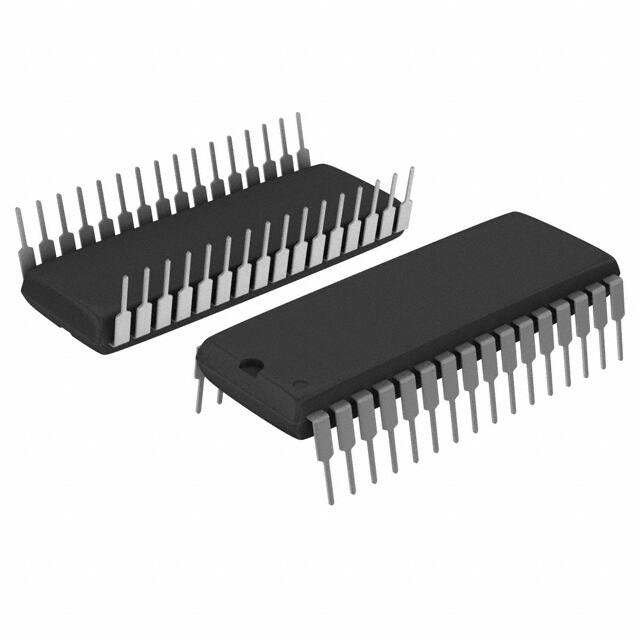
approved 32-pin DIP, PLCC and TSOP packages.
The CAT28C512/513 is a fast,low power, 5V-only CMOS
parallel EEPROM organized as 64K x 8-bits. It requires
a simple interface for in-system programming. On-chip
address and data latches, self-timed write cycle with
auto-clear and VCC power up/down write protection
eliminate additional timing and protection hardware.
DATA Polling and Toggle status bits signal the start and
end of the self-timed write cycle. Additionally, the
CAT28C512/513 features hardware and software write
protection.
BLOCK DIAGRAM
A7–A15
ADDR. BUFFER
& LATCHES
ROW
DECODER
VCC
INADVERTENT
WRITE
PROTECTION
HIGH VOLTAGE
GENERATOR
CE
OE
WE
CONTROL
128 BYTE PAGE
REGISTER
I/O BUFFERS
TIMER
A0–A6
65,536 x 8
EEPROM
ARRAY
DATA POLLING
AND
TOGGLE BIT
ADDR. BUFFER
& LATCHES
© 2009 SCILLC. All rights reserved.
Characteristics subject to change without notice
I/O0–I/O7
COLUMN
DECODER
1
Doc. No. MD-1007, Rev. I
�CAT28C512/513
PIN CONFIGURATION
15
16
A13
A8
A9
A11
OE
A10
CE
I/O7
A2
A1
A0
I/O0
I/O6
I/O5
I/O4
I/O3
A13
VCC
WE
A15
A7
A12
NC
NC
VCC
WE
A12
A15
NC
4 3 2 1 32 31 30
5
29
6
28
7
27
8
26
CAT28C512
9
25
TOP VIEW
10
24
11
23
12
22
13
21
14 15 16 17 18 19 20
A7
A6
A5
A4
A3
4 3 2 1 32 31 30
A14
A13
A6
A5
5
6
29
28
A8
A9
A4
A3
A11
OE
A10
A2
A1
A0
7
8
9
10
27
26
25
24
CE
I/O7
NC
I/O0
CAT28C513
TOP VIEW
11
23
12
22
13
21
14 15 16 17 18 19 20
A8
A9
A11
NC
OE
A10
CE
I/O7
I/O6
NC
I/O3
I/O4
I/O5
I/O1
I/O2
VSS
30
29
28
27
26
25
24
23
22
21
20
19
18
17
VCC
WE
NC
A14
I/O1
I/O2
VSS
A12
A7
A6
A5
A4
A3
A2
A1
A0
I/O0
32
31
I/O6
A15
1
2
3
4
5
6
7
8
9
10
11
12
13
14
I/O1
I/O2
VSS
I/O3
I/O4
I/O5
NC
NC
PLCC Package (N, G)
PLCC Package (N, G)
A14
DIP Package (L)
TSOP Package (8mmx20mm) (T, H)
A11
A9
A8
A13
A14
NC
WE
VCC
NC
NC
A15
A12
A7
A6
A5
A4
1
2
3
4
5
6
7
8
9
10
11
12
13
14
15
16
32
31
30
29
28
27
26
25
24
23
22
21
20
19
18
17
CAT28C512
TOP VIEW
OE
A10
CE
I/O7
I/O6
I/O5
I/O4
I/O3
Vss
I/O2
I/O1
I/O0
A0
A1
A2
A3
PIN FUNCTIONS
Pin Name
Function
Pin Name
Function
A0–A15
Address Inputs
WE
Write Enable
I/O0–I/O7
Data Inputs/Outputs
VCC
5V Supply
CE
Chip Enable
VSS
Ground
OE
Output Enable
NC
No Connect
Doc. No. MD-1007, Rev. I
2
© 2009 SCILLC. All rights reserved.
Characteristics subject to change without notice
�CAT28C512/513
ABSOLUTE MAXIMUM RATINGS*
*COMMENT
Temperature Under Bias ................. –55°C to +125°C
Stresses above those listed under “Absolute Maximum
Ratings” may cause permanent damage to the device.
These are stress ratings only, and functional operation
of the device at these or any other conditions outside of
those listed in the operational sections of this specification is not implied. Exposure to any absolute maximum
rating for extended periods may affect device performance and reliability.
Storage Temperature ....................... –65°C to +150°C
Voltage on Any Pin with
Respect to Ground(2) ........... –2.0V to +VCC + 2.0V
VCC with Respect to Ground ............... –2.0V to +7.0V
Package Power Dissipation
Capability (Ta = 25°C) ................................... 1.0W
Lead Soldering Temperature (10 secs) ............ 300°C
Output Short Circuit Current(3) ........................ 100 mA
RELIABILITY CHARACTERISTICS
Symbol
Parameter
Min
Max.
Units
Test Method
100,000
Cycles/Byte
MIL-STD-883, Test Method 1033
NEND(1)
Endurance
TDR(1)
Data Retention
100
Years
MIL-STD-883, Test Method 1008
VZAP(1)
ESD Susceptibility
2000
Volts
MIL-STD-883, Test Method 3015
ILTH(1)(4)
Latch-Up
100
mA
JEDEC Standard 17
D.C. OPERATING CHARACTERISTICS
VCC = 5V ±10%, unless otherwise specified.
Limits
Symbol
Parameter
Min
Typ
Max.
Units
Test Conditions
ICC
VCC Current (Operating, TTL)
50
mA
CE = OE = VIL, f=6MHz
All I/O’s Open
ICCC(5)
VCC Current (Operating, CMOS)
25
mA
CE = OE = VILC, f=6MHz
All I/O’s Open
ISB
VCC Current (Standby, TTL)
3
mA
CE = VIH, All I/O’s Open
ISBC(6)
VCC Current (Standby, CMOS)
200
µA
CE = VIHC,
All I/O’s Open
ILI
Input Leakage Current
-10
10
µA
VIN = GND to VCC
ILO
Output Leakage Current
-10
10
µA
VOUT = GND to VCC,
CE = VIH
VIH(6)
High Level Input Voltage
2
VCC +0.3
V
VIL(5)
Low Level Input Voltage
-1
0.8
V
VOH
High Level Output Voltage
2.4
VOL
Low Level Output Voltage
VWI
Write Inhibit Voltage
0.4
3.5
V
IOH = –400µA
V
IOL = 2.1mA
V
Note:
(1) This parameter is tested initially and after a design or process change that affects the parameter.
(2) The minimum DC input voltage is –0.5V. During transitions, inputs may undershoot to –2.0V for periods of less than 20 ns. Maximum DC
voltage on output pins is VCC +0.5V, which may overshoot to VCC +2.0V for periods of less than 20 ns.
(3) Output shorted for no more than one second. No more than one output shorted at a time.
(4) Latch-up protection is provided for stresses up to 100mA on address and data pins from –1V to VCC +1V.
(5) VILC = –0.3V to +0.3V.
(6) VIHC = VCC –0.3V to VCC +0.3V.
© 2009 SCILLC. All rights reserved.
Characteristics subject to change without notice
3
Doc. No. MD-1007, Rev . I
�CAT28C512/513
MODE SELECTION
Mode
CE
WE
OE
Read
L
H
Byte Write (WE Controlled)
L
Byte Write (CE Controlled)
I/O
Power
L
DOUT
ACTIVE
H
DIN
ACTIVE
L
H
DIN
ACTIVE
Standby, and Write Inhibit
H
X
X
High-Z
STANDBY
Read and Write Inhibit
X
H
H
High-Z
ACTIVE
Test
Max.
Units
Conditions
Input/Output Capacitance
10
pF
VI/O = 0V
Input Capacitance
6
pF
VIN = 0V
CAPACITANCE TA = 25°C, f = 1.0 MHz, VCC = 5V
Symbol
CI/O
(1)
CIN(1)
A.C. CHARACTERISTICS, Read Cycle
VCC=5V + 10%, Unless otherwise specified
28C512/513-12 28C512/513-15
Symbol
Parameter
Min.
Max.
Min.
Max.
tRC
Read Cycle Time
120
tCE
CE Access Time
120
150
ns
tAA
Address Access Time
120
150
ns
tOE
OE Access Time
50
70
ns
tLZ(1)
CE Low to Active Output
0
0
ns
tOLZ(1)
OE Low to Active Output
0
0
ns
tHZ(1)(2)
CE High to High-Z Output
50
50
ns
tOHZ(1)(2)
OE High to High-Z Output
50
50
ns
tOH(1)
Output Hold from Address Change
150
0
Units
ns
0
ns
Power-Up Timing
Symbol
Parameter
tPUR (1)
Power-up to Read Operation
tPUW (2)
Power-up to Write Operation
Min.
5
Max
Units
100
µs
10
ms
Note:
(1) This parameter is tested initially and after a design or process change that affects the parameter.
(2) Output floating (High-Z) is defined as the state when the external data line is no longer driven by the output buffer.
Doc. No. MD-1007, Rev. I
4
© 2009 SCILLC. All rights reserved.
Characteristics subject to change without notice
�CAT28C512/513
A.C. CHARACTERISTICS, Write Cycle
VCC=5V+10%, unless otherwise specified
28C512/513-12 28C512/513-15
Min. Max. Min. Max. Units
Symbol
Parameter
tWC
Write Cycle Time
tAS
Address Setup Time
0
0
ns
tAH
Address Hold Time
50
50
ns
tCS
CE Setup Time
0
0
ns
CE Hold Time
0
0
ns
CE Pulse Time
100
100
ns
tOES
OE Setup Time
0
0
ns
tOEH
OE Hold Time
0
0
ns
tWP(3)
WE Pulse Width
100
100
ns
tDS
Data Setup Time
50
50
ns
tDH
Data Hold Time
0
0
ns
tINIT(1)
Write Inhibit Period After Power-up
5
10
5
10
ms
0.1
100
0.1
100
µs
tCH
tCW
(3)
5
tBLC(1)(4) Byte Load Cycle Time
5
ms
Figure 1. A.C. Testing Input/Output Waveform(2)
VCC - 0.3V
2.0 V
INPUT PULSE LEVELS
REFERENCE POINTS
0.8 V
0.0 V
Figure 2. A.C. Testing Load Circuit (example)
1.3V
1N914
3.3K
DEVICE
UNDER
TEST
OUT
CL = 100 pF
CL INCLUDES JIG CAPACITANCE
Note:
(1) This parameter is tested initially and after a design or process change that affects the parameter.
(2) Input rise and fall times (10% and 90%) < 10 ns.
(3) A write pulse of less than 20ns duration will not initiate a write cycle.
(4) A timer of duration tBLC max. begins with every LOW to HIGH transition of WE. If allowed to time out, a page or byte write will begin;
however a transition from HIGH to LOW within tBLC max. stops the timer.
© 2009 SCILLC. All rights reserved.
Characteristics subject to change without notice
5
Doc. No. MD-1007, Rev . I
�CAT28C512/513
Byte Write
DEVICE OPERATION
A write cycle is executed when both CE and WE are low,
and OE is high. Write cycles can be initiated using either
WE or CE, with the address input being latched on the
falling edge of WE or CE, whichever occurs last. Data,
conversely, is latched on the rising edge of WE or CE,
whichever occurs first. Once initiated, a byte write cycle
automatically erases the addressed byte and the new
data is written within 5 ms.
Read
Data stored in the CAT28C512/513 is transferred to the
data bus when WE is held high, and both OE and CE
are held low. The data bus is set to a high impedance
state when either CE or OE goes high. This 2-line control
architecture can be used to eliminate bus contention in
a system environment.
Figure 3. Read Cycle
tRC
ADDRESS
tCE
CE
tOE
OE
VIH
tLZ
WE
tOHZ
DATA OUT
tHZ
tOH
tOLZ
HIGH-Z
DATA VALID
DATA VALID
tAA
Figure 4. Byte Write Cycle [WE Controlled]
tWC
ADDRESS
tAS
tAH
tCH
tCS
CE
OE
tOES
tWP
tOEH
WE
tBLC
DATA OUT
DATA IN
HIGH-Z
DATA VALID
tDS
Doc. No. MD-1007, Rev. I
tDH
6
© 2009 SCILLC. All rights reserved.
Characteristics subject to change without notice
�CAT28C512/513
Page Write
to A6 (which can be loaded in any order) during the first
and subsequent write cycles. Each successive byte load
cycle must begin within tBLC MAX of the rising edge of the
preceding WE pulse. There is no page write window
limitation as long as WE is pulsed low within tBLC MAX.
The page write mode of the CAT28C512/513 (essentially an extended BYTE WRITE mode) allows from 1 to
128 bytes of data to be programmed within a single
EEPROM write cycle. This effectively reduces the bytewrite time by a factor of 128.
Upon completion of the page write sequence, WE must
stay high a minimum of tBLC MAX for the internal automatic program cycle to commence. This programming
cycle consists of an erase cycle, which erases any data
that existed in each addressed cell, and a write cycle,
which writes new data back into the cell. A page write will
only write data to the locations that were addressed and
will not rewrite the entire page.
Following an initial WRITE operation (WE pulsed low, for
tWP, and then high) the page write mode can begin by
issuing sequential WE pulses, which load the address
and data bytes into a 128 byte temporary buffer. The
page address where data is to be written, specified by
bits A7 to A15, is latched on the last falling edge of WE.
Each byte within the page is defined by address bits A0
CE Controlled]
Figure 5. Byte Write Cycle [CE
tWC
ADDRESS
tAS
tAH
tBLC
tCW
CE
tOEH
OE
tCS
tOES
tCH
WE
HIGH-Z
DATA OUT
DATA IN
DATA VALID
tDS
tDH
Figure 6. Page Mode Write Cycle
OE
CE
t BLC
t WP
WE
ADDRESS
t WC
I/O
LAST BYTE
BYTE 0
© 2009 SCILLC. All rights reserved.
Characteristics subject to change without notice
BYTE 1
BYTE 2
7
BYTE n
BYTE n+1
BYTE n+2
Doc. No. MD-1007, Rev . I
�CAT28C512/513
DATA Polling
Toggle Bit
DATA polling is provided to indicate the completion of
write cycle. Once a byte write or page write cycle is
initiated, attempting to read the last byte written will
output the complement of that data on I/O7 (I/O0–I/O6
are indeterminate) until the programming cycle is complete. Upon completion of the self-timed write cycle, all
I/O’s will output true data during a read cycle.
In addition to the DATA Polling feature of the CAT28C512/
513, the device offers an additional method for determining the completion of a write cycle. While a write cycle is
in progress, reading data from the device will result in I/
O6 toggling between one and zero. However, once the
write is complete, I/O6 stops toggling and valid data can
be read from the device.
Figure 7. DATA Polling
ADDRESS
CE
WE
tOEH
tOES
tOE
OE
tWC
I/O7
DIN = X
DOUT = X
D OUT = X
Figure 8. Toggle Bit
WE
CE
tOEH
tOES
tOE
OE
I/O6
(1)
(1)
tWC
Note:
(1) Beginning and ending state of I/O6 is indeterminate.
Doc. No. MD-1007, Rev. I
8
© 2009 SCILLC. All rights reserved.
Characteristics subject to change without notice
�CAT28C512/513
HARDWARE DATA PROTECTION
The following is a list of hardware data protection features that are incorporated into the CAT28C512/513.
(4) Noise pulses of less than 20 ns on the WE or CE
inputs will not result in a write cycle.
(1) VCC sense provides for write protection when VCC
falls below 3.5V min.
SOFTWARE DATA PROTECTION
The CAT28C512/513 features a software controlled
data protection scheme which, once enabled, requires a
data algorithm to be issued to the device before a write
can be performed. The device is shipped from Catalyst
with the software protection NOT ENABLED (the
CAT28C512/513 is in the standard operating mode).
(2) A power on delay mechanism, tINIT (see AC characteristics), provides a 5 to 10 ms delay before a write
sequence, after VCC has reached 3.5V min.
(3) Write inhibit is activated by holding any one of OE
low, CE high or WE high.
Figure 9. Write Sequence for Activating Software
Data Protection
WRITE DATA:
ADDRESS:
WRITE DATA:
ADDRESS:
WRITE DATA:
ADDRESS:
Figure 10. Write Sequence for Deactivating
Software Data Protection
WRITE DATA:
AA
ADDRESS:
5555
WRITE DATA:
55
ADDRESS:
2AAA
WRITE DATA:
A0
ADDRESS:
5555
(1)
SOFTWARE DATA
(12)
PROTECTION ACTIVATED
WRITE DATA:
WRITE DATA:
XX
WRITE DATA:
TO ANY ADDRESS
ADDRESS:
WRITE LAST BYTE
TO
LAST ADDRESS
W R I T E DATA :
ADDRESS:
ADDRESS:
AA
5555
55
2AAA
80
5555
AA
5555
55
2AAA
20
5555
Note:
(1) Write protection is activated at this point whether or not any more writes are completed. Writing to addresses must occur within tBLC
Max., after SDP activation.
© 2009 SCILLC. All rights reserved.
Characteristics subject to change without notice
9
Doc. No. MD-1007, Rev . I
�CAT28C512/513
To activate the software data protection, the device must
be sent three write commands to specific addresses with
specific data (Figure 9). This sequence of commands
(along with subsequent writes) must adhere to the page
write timing specifications (Figure 11). Once this is done,
all subsequent byte or page writes to the device must be
preceded by this same set of write commands. The data
protection mechanism is activated until a deactivate
sequence is issued regardless of power on/off transitions. This gives the user added inadvertent write protection on power-up in addition to the hardware protection provided.
To allow the user the ability to program the device with
an EEPROM programmer (or for testing purposes) there
is a software command sequence for deactivating the
data protection. The six step algorithm (Figure 10) will
reset the internal protection circuitry, and the device will
return to standard operating mode (Figure 12 provides
reset timing). After the sixth byte of this reset sequence
has been issued, standard byte or page writing can
commence.
Figure 11. Software Data Protection Timing
DATA
ADDRESS
AA
5555
55
2AAA
tWC
A0
5555
BYTE OR
PAGE
CE
tWP
tBLC
WRITES
ENABLED
WE
Figure 12. Resetting Software Data Protection Timing
DATA
ADDRESS
AA
5555
55
2AAA
80
5555
AA
5555
55
2AAA
20
5555
tWC
SDP
RESET
CE
DEVICE
UNPROTECTED
WE
Doc. No. MD-1007, Rev. I
10
© 2009 SCILLC. All rights reserved.
Characteristics subject to change without notice
�CAT28C512/513
(1)
EXAMPLE OF ORDERING INFORMATION
Prefix
Device #
CAT
28C512
Optional
Company
ID
Suffix
N
-15
I
Temperature Range
Blank = Commercial (0°C to +70°C)
I = Industrial (-40°C to +85°C)
(4)
A = Automotive (-40°C to +105°C)
Product
Number
28C512
28C513
Package
N: PLCC(2)
T: TSOP (8mmx20mm)(2)
L: PDIP (Lead free, Halogen free)
(3)
G: PLCC (Lead free, Halogen free)
H: TSOP (8mmx20mm) (Lead free, Halogen free)
T
Tape & Reel
Speed
12: 120ns
15: 150ns
ORDERING INFORMATION
Orderable Part Numbers (for Pb-Free Devices)
CAT28C512G-12T
CAT28C513G-12T
CAT28C512G-15T
CAT28C513G-15T
CAT28C512GA-12T
CAT28C513GA-12T
CAT28C512GA-15T
CAT28C513GA-15T
CAT28C512GI-12T
CAT28C513GI-12T
CAT28C512GI-15T
CAT28C513GI-15T
CAT28C512H-12T
CAT28C512H-15T
CAT28C512HA-12T
CAT28C512HA-15T
CAT28C512HI-12T
CAT28C512HI-15T
CAT28C512L12
CAT28C512L15
CAT28C512LA12
CAT28C512LA15
CAT28C512LI12
CAT28C512LI15
Notes:
(1) The device used in the above example is a CAT28C512NI-15T (PLCC, Industrial temperature, 150 ns Access Time, Tape & Reel).
(2) Solder-plate (tin-lead) packages, contact Factory for availability.
(3) 28C513 is offered only in PLCC package.
(4) -40°C to +125°C is available upon request.
© 2009 SCILLC. All rights reserved.
Characteristics subject to change without notice
11
Doc. No. MD-1007, Rev . I
�CAT28C512/513
REVISION HISTORY
Date
Revision Description
19-Apr-04
E
Delete data sheet designation
Update Block Diagram
Update Ordering Information
Add Revision History
Update Rev Number
17-Nov-04
F
Delete T14 and H14 package codes
15-Oct-08
G
Eliminate PDIP SnPb package
20-Nov-08
H
Change logo and fine print to ON Semiconductor
I
Update Example of Ordering Information
Update Ordering Information table
28-Jul-09
ON Semiconductor and
are registered trademarks of Semiconductor Components Industries, LLC (SCILLC). SCILLC reserves the right to make changes without further notice to
any products herein. SCILLC makes no warranty, representation or guarantee regarding the suitability of its products for any particular purpose, nor does SCILLC assume any liability arising
out of the application or use of any product or circuit, and specifically disclaims any and all liability, including without limitation special, consequential or incidental damages.
“Typical” parameters which may be provided in SCILLC data sheets and/or specifications can and do vary in different applications and actual performance may vary over time. All
operating parameters, including “Typicals” must be validated for each customer application by customer’s technical experts. SCILLC does not convey any license under its patent rights nor the rights
of others. SCILLC products are not designed, intended, or authorized for use as components in systems intended for surgical implant into the body, or other applications
intended to support or sustain life, or for any other application in which the failure of the SCILLC product could create a situation where personal injury or death may occur. Should
Buyer purchase or use SCILLC products for any such unintended or unauthorized application, Buyer shall indemnify and hold SCILLC and its officers, employees, subsidiaries, affiliates,
and distributors harmless against all claims, costs, damages, and expenses, and reasonable attorney fees arising out of, directly or indirectly, any claim of personal injury or death
associated with such unintended or unauthorized use, even if such claim alleges that SCILLC was negligent regarding the design or manufacture of the part. SCILLC is an Equal
Opportunity/Affirmative Action Employer. This literature is subject to all applicable copyright laws and is not for resale in any manner.
PUBLICATION ORDERING INFORMATION
LITERATURE FULFILLMENT:
Literature Distribution Center for ON Semiconductor
P.O. Box 5163, Denver, Colorado 80217 USA
Phone: 303-675-2175 or 800-344-3860 Toll Free USA/Canada
Fax: 303-675-2176 or 800-344-3867 Toll Free USA/Canada
Email: orderlit@onsemi.com
Doc. No. MD-1007, Rev. I
N. American Technical Support: 800-282-9855
Toll Free
USA/Canada
Europe, Middle East and Africa Technical Support:
Phone: 421 33 790 2910
Japan Customer Focus Center:
Phone: 81-3-5773-3850
12
ON Semiconductor Website: www.onsemi.com
Order Literature: http://www.onsemi.com/orderlit
For additional information, please contact your local
Sales Representative
© 2009 SCILLC. All rights reserved.
Characteristics subject to change without notice
�


 工商网监
湘ICP备2023018690号
工商网监
湘ICP备2023018690号
