ON Semiconductor
Is Now
To learn more about onsemi™, please visit our website at
www.onsemi.com
onsemi and and other names, marks, and brands are registered and/or common law trademarks of Semiconductor Components Industries, LLC dba “onsemi” or its affiliates and/or
subsidiaries in the United States and/or other countries. onsemi owns the rights to a number of patents, trademarks, copyrights, trade secrets, and other intellectual property. A listing of onsemi
product/patent coverage may be accessed at www.onsemi.com/site/pdf/Patent-Marking.pdf. onsemi reserves the right to make changes at any time to any products or information herein, without
notice. The information herein is provided “as-is” and onsemi makes no warranty, representation or guarantee regarding the accuracy of the information, product features, availability, functionality,
or suitability of its products for any particular purpose, nor does onsemi assume any liability arising out of the application or use of any product or circuit, and specifically disclaims any and all
liability, including without limitation special, consequential or incidental damages. Buyer is responsible for its products and applications using onsemi products, including compliance with all laws,
regulations and safety requirements or standards, regardless of any support or applications information provided by onsemi. “Typical” parameters which may be provided in onsemi data sheets and/
or specifications can and do vary in different applications and actual performance may vary over time. All operating parameters, including “Typicals” must be validated for each customer application
by customer’s technical experts. onsemi does not convey any license under any of its intellectual property rights nor the rights of others. onsemi products are not designed, intended, or authorized
for use as a critical component in life support systems or any FDA Class 3 medical devices or medical devices with a same or similar classification in a foreign jurisdiction or any devices intended for
implantation in the human body. Should Buyer purchase or use onsemi products for any such unintended or unauthorized application, Buyer shall indemnify and hold onsemi and its officers, employees,
subsidiaries, affiliates, and distributors harmless against all claims, costs, damages, and expenses, and reasonable attorney fees arising out of, directly or indirectly, any claim of personal injury or death
associated with such unintended or unauthorized use, even if such claim alleges that onsemi was negligent regarding the design or manufacture of the part. onsemi is an Equal Opportunity/Affirmative
Action Employer. This literature is subject to all applicable copyright laws and is not for resale in any manner. Other names and brands may be claimed as the property of others.
�CAT34TS02
Digital Output Temperature
Sensor with On-board SPD
EEPROM
Description
The CAT34TS02 combines a JC42.4 compliant Temperature Sensor
(TS) with 2−Kb of Serial Presence Detect (SPD) EEPROM.
The TS measures temperature at least 10 times every second.
Temperature readings can be retrieved by the host via the serial
interface, and are compared to high, low and critical trigger limits
stored into internal registers. Over or under limit conditions can be
signaled on the open−drain EVENT pin.
The integrated 2−Kb SPD EEPROM is internally organized as 16
pages of 16 bytes each, for a total of 256 bytes. It features a page write
buffer and supports both the Standard (100 kHz) as well as Fast
(400 kHz) I2C protocol.
Write operations to the lower half memory can be inhibited via
software commands. The CAT34TS02 features Permanent, as well as
Reversible Software Write Protection, as defined for DDR3 DIMMs.
http://onsemi.com
PIN CONFIGURATION
A0
•
•
•
1
VCC
A1
EVENT
A2
SCL
VSS
SDA
(Top View)
Features
•
•
•
•
•
•
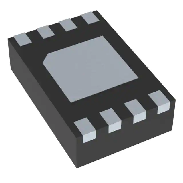
UDFN−8
HU4 SUFFIX
CASE 517AZ
TDFN−8
VP2 SUFFIX
CASE 511AK
JEDEC JC42.4 Compliant Temperature Sensor
Temperature Range: −20°C to +125°C
DDR3 DIMM Compliant SPD EEPROM
Supply Range: 3.3 V ± 10%
I2C / SMBus Interface
Schmitt Triggers and Noise Suppression Filters on SCL and SDA
Inputs
Low Power CMOS Technology
2 x 3 x 0.75 mm TDFN Package and 2 x 3 x 0.5 mm UDFN Package
These Devices are Pb−Free and are RoHS Compliant
VCC
For the location of Pin 1, please consult the
corresponding package drawing.
MARKING DIAGRAM
TDFN−8
GTX
ALL
YM
G
TSU
ALL
YM
G
GTX, TSU = Specific Device Code
A
= Assembly Location Code
LL
= Assembly Lot Number (Last Two Digits)
Y
= Production Year (Last Digit)
M
= Production Month (1 − 9, O, N, D)
G
= Pb−Free Package
SCL
PIN FUNCTIONS
Pin Name
CAT34TS02
A2, A1, A0
UDFN−8
EVENT
A0, A1, A2
SDA
Function
Device Address Input
SDA
Serial Data Input/Output
SCL
Serial Clock Input
EVENT
Open−drain Event Output
VSS
VCC
Power Supply
Figure 1. Functional Symbol
VSS
Ground
DAP
Backside Exposed DAP at VSS
ORDERING INFORMATION
See detailed ordering and shipping information in the package
dimensions section on page 21 of this data sheet.
© Semiconductor Components Industries, LLC, 2014
June, 2014 − Rev. 12
1
Publication Order Number:
CAT34TS02/D
�CAT34TS02
Table 1. ABSOLUTE MAXIMUM RATINGS
Parameter
Rating
Units
Operating Temperature
−45 to +130
°C
Storage Temperature
−65 to +150
°C
Voltage on any pin (except A0) with respect to Ground (Note 1)
−0.5 to +6.5
V
Voltage on pin A0 with respect to Ground
−0.5 to +10.5
V
Stresses exceeding those listed in the Maximum Ratings table may damage the device. If any of these limits are exceeded, device functionality
should not be assumed, damage may occur and reliability may be affected.
1. The DC input voltage on any pin should not be lower than −0.5 V or higher than VCC + 0.5 V. The A0 pin can be raised to a HV level for RSWP
command execution. SCL and SDA inputs can be raised to the maximum limit, irrespective of VCC.
Table 2. RELIABILITY CHARACTERISTICS
Symbol
Parameter
NEND (Note 2)
Endurance (EEPROM)
TDR
Data Retention (EEPROM)
Min
Units
1,000,000
Write Cycles
100
Years
2. Page Mode, VCC = 3.3 V, 25°C
Table 3. TEMPERATURE CHARACTERISTICS (VCC = 3.3 V ± 10%, TA = −20°C to +125°C, unless otherwise specified)
Parameter
Temperature Reading Error
Class B, JC42.4 compliant
Test Conditions/Comments
Max
Unit
+75°C ≤ TA ≤ +95°C, active range
±1.0
°C
+40°C ≤ TA ≤ +125°C, monitor range
±2.0
°C
−20°C ≤ TA ≤ +125°C, sensing range
±3.0
°C
ADC Resolution
Temperature Resolution
Conversion Time
Thermal Resistance (Note 3) qJA
Junction−to−Ambient (Still Air)
12
Bits
0.0625
°C
100
ms
92
°C/W
3. Power Dissipation is defined as PJ = (TJ − TA)/qJA, where TJ is the junction temperature and TA is the ambient temperature. The thermal
resistance value refers to the case of a package being used on a standard 2−layer PCB.
Table 4. D.C. OPERATING CHARACTERISTICS (VCC = 3.3 V ± 10%, TA = −20°C to +125°C, unless otherwise specified)
Symbol
Max
Unit
TS active, SPD and Bus idle
500
mA
SPD Write, TS shut−down
500
mA
Standby Current
TS shut−down; SPD and Bus idle
10
mA
ILKG
I/O Pin Leakage Current
Pin at GND or VCC
2
mA
ICC
ISHDN
Parameter
Supply Current
Test Conditions/Comments
Min
VIL
Input Low Voltage
−0.5
0.3 x VCC
V
VIH
Input High Voltage
0.7 x VCC
VCC + 0.5
V
VOL1
Output Low Voltage
IOL = 3 mA, VCC > 2.7 V
0.4
V
VOL2
Output Low Voltage
IOL = 1 mA, VCC < 2.7 V
0.2
V
Product parametric performance is indicated in the Electrical Characteristics for the listed test conditions, unless otherwise noted. Product
performance may not be indicated by the Electrical Characteristics if operated under different conditions.
http://onsemi.com
2
�CAT34TS02
Table 5. PIN IMPEDANCE CHARACTERISTICS (VCC = 3.3 V ± 10%, TA = −20°C to +125°C, unless otherwise specified)
Parameter
Symbol
CIN
(Note 4)
SDA, EVENT Pin Capacitance
IA
(Note 5)
Address Input Current (A0, A1, A2)
Product Rev C
Conditions
Max
Units
VIN = 0 V, f = 1 MHz
8
pF
Input Capacitance (other pins)
6
VIN < VIH
35
VIN > VIH
2
mA
4. These parameters are tested initially and after a design or process change that affects the parameter according to appropriate AEC−Q100
and JEDEC test methods.
5. When not driven, the A0, A1 and A2 pins are pulled down to GND internally. For improved noise immunity, the internal pull-down is relatively
strong; therefore the external driver must be able to supply the pull-down current when attempting to drive the input HIGH. To conserve power,
as the input level exceeds the trip point of the CMOS input buffer (~ 0.5 x VCC), the strong pull-down reverts to a weak current source.
Table 6. A.C. CHARACTERISTICS (VCC = 3.3 V ± 10%, TA = −20°C to +125°C) (Note 6)
Symbol
Min
Max
Units
Clock Frequency
10
400
kHz
tHIGH
High Period of SCL Clock
600
ns
tLOW
Low Period of SCL Clock
1300
ns
FSCL (Note 7)
tTIMEOUT (Note 7)
Parameter
SMBus SCL Clock Low Timeout
tR (Note 8)
SDA and SCL Rise Time
tF (Note 8)
SDA and SCL Fall Time
tSU:DAT (Note 9)
25
35
ms
300
ns
300
ns
Data Setup Time
100
ns
tSU:STA
START Condition Setup Time
600
ns
tHD:STA
START Condition Hold Time
600
ns
tSU:STO
STOP Condition Setup Time
600
ns
Bus Free Time Between STOP and START
1300
ns
tBUF
tHD:DAT
tDH (Note 8)
Ti
tWR
tPU (Note 10)
Input Data Hold Time
0
Output Data Hold Time
200
Noise Pulse Filtered at SCL and SDA Inputs
Write Cycle Time
Power−up Delay to Valid Temperature Recording
ns
900
ns
100
ns
5
ms
100
ms
6. Timing reference points are set at 30%, respectively 70% of VCC, as illustrated in Figure 23. Bus loading must be such as to allow meeting
the VIL, VOL as well as the various timing limits.
7. For the CAT34TS02 Rev. B, the TS interface will reset itself and will release the SDA line if the SCL line stays low beyond the tTIMEOUT limit.
The time−out count−down is activated in the interval between START and STOP when SCL is low and is reset while SCL is high. The minimum
clock frequency of 10 kHz is an SMBus recommendation; the minimum operating clock frequency for the CAT34TS02’s SPD component
is DC, while the minimum operating frequency for the TS component is limited only by the SMBus time−out. For the CAT34TS02 Rev. C,
both the TS and the SPD implement the time−out feature.
8. In a “Wired−OR” system (such as I2C or SMBus), SDA rise time is determined by bus loading. Since each bus pull−down device must be
able to sink the (external) bus pull−up current (in order to meet the VIL and/or VOL limits), it follows that SDA fall time is inherently faster than
SDA rise time. SDA rise time can exceed the standard recommended tR limit, as long as it does not exceed tLOW − tDH − tSU:DAT, where tLOW
and tDH are actual values (rather than spec limits). A shorter tDH leaves more room for a longer SDA tR, allowing for a more capacitive bus
or a larger bus pull−up resistor. At the minimum tLOW spec limit of 1300 ns, the maximum tDH of 900 ns demands a maximum SDA tR of 300 ns.
The CAT34TS02’s maximum tDH is


 工商网监
湘ICP备2023018690号
工商网监
湘ICP备2023018690号
