www.fairchildsemi.com
LM324/LM324A, LM2902/LM2902A
Quad Operational Amplifier
Features
Description
• Internally Frequency Compensated for Unity Gain
• Large DC Voltage Gain: 100dB
• Wide Power Supply Range:
LM324/LM324A : 3V~32V (or ±1.5 ~ 16V)
LM2902/LM2902A: 3V~26V (or ±1.5V ~ 13V)
• Input Common Mode Voltage Range Includes
Ground
• Large Output Voltage Swing: 0V to VCC -1.5V
• Power Drain Suitable for Battery Operation
The LM324/LM324A, LM2902/LM2902A consist of four
independent, high gain, internally frequency compensated operational amplifiers which were designed specifically to operate from a single power supply over a
wide voltage range. operation from split power supplies
is also possible so long as the difference between the
two supplies is 3 volts to 32 volts. Application areas
include transducer amplifier, DC gain blocks and all the
conventional OP Amp circuits which now can be easily
implemented in single power supply systems.
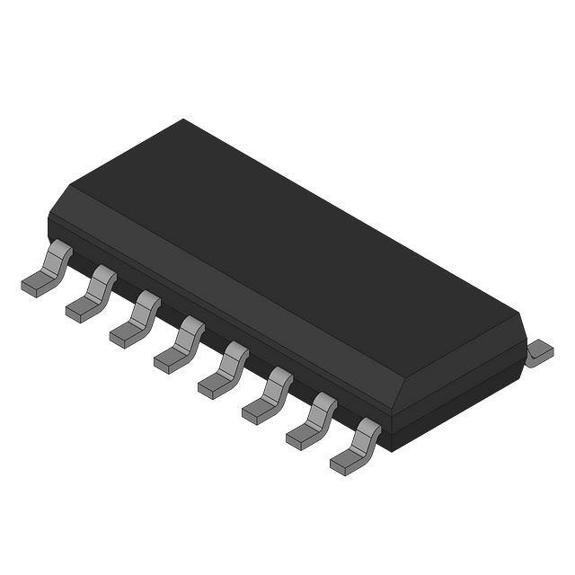
14-DIP
1
14-SOP
1
Internal Block Diagram
14 OUT4
OUT1 1
IN1 (-)
2
IN1 (+) 3
1
_ +
+
4
_
13 IN4 (-)
12 IN4 (+)
VCC 4
11 GND
IN2 (+)
5
_ +
IN2 (-)
6
2
OUT2
7
+
_
10 IN3 (+)
3
9 IN3 (-)
8 OUT3
Rev. 1.0.9
©2012 Fairchild Semiconductor Corporation
�LM324/LM324A, LM2902/LM2902A
Schematic Diagram
(One Section Only)
VCC
Q5
Q12
Q6
Q17
Q19
Q20
Q2
Q3
R1
C1
Q4
IN(-)
Q18
Q1
R2
IN(+)
Q11
OUTPUT
Q21
Q10
Q7
Q8
Q9
Q15
Q13
Q14
Q16
GND
Absolute Maximum Ratings
Parameter
Symbol
LM324/LM324A
LM2902/LM2902A
Unit
VCC
±16 or 32
±13 or 26
V
VI(DIFF)
32
26
V
Input Voltage
VI
-0.3 to +32
-0.3 to +26
V
Output Short Circuit to GND
Vcc≤15V, TA=25°C(one Amp)
-
Continuous
Continuous
-
PD
1310
640
1310
640
mW
Operating Temperature Range
TOPR
0 ~ +70
-40 ~ +85
°C
Storage Temperature Range
TSTG
-65 ~ +150
-65 ~ +150
°C
Power Supply Voltage
Differential Input Voltage
Power Dissipation, TA=25°C
14-DIP
14-SOP
Thermal Data
Parameter
Thermal Resistance Junction-Ambient Max.
14-DIP
14-SOP
2
Symbol
Value
Unit
Rθja
95
195
°C/W
�LM324/LM324A, LM2902/LM2902A
Electrical Characteristics
(VCC = 5.0V, VEE = GND, TA = 25°C, unless otherwise specified)
Parameter
Symbol
Conditions
Input Offset Voltage
VIO
Input Offset Current
LM324
LM2902
Unit
Min.
Typ.
Max.
Min.
Typ.
Max.
VCM = 0V to VCC -1.5V
VO(P) = 1.4V, RS = 0Ω
(Note1)
-
1.5
7.0
-
1.5
7.0
mV
IIO
VCM = 0V
-
3.0
50
-
3.0
50
nA
Input Bias Current
IBIAS
VCM = 0V
-
40
250
-
40
250
nA
Input Common-Mode
Voltage Range
VI(R)
Note1
0
-
VCC
-1.5
0
-
VCC
-1.5
V
Supply Current
ICC
RL = ∞,VCC = 30V
(LM2902,VCC=26V)
-
1.0
3
-
1.0
3
mA
RL = ∞,VCC = 5V
-
0.7
1.2
-
0.7
1.2
mA
VCC = 15V,RL=2kΩ
VO(P) = 1V to 11V
25
100
-
25
100
-
V/mV
RL = 2kΩ
26
-
-
22
-
-
V
RL=10kΩ
27
28
-
23
24
-
V
-
5
20
-
5
100
mV
Large Signal
Voltage Gain
Output Voltage Swing
GV
VO(H)
Note1
VO(L)
VCC = 5V, RL=10kΩ
Common-Mode
Rejection Ratio
CMRR
-
65
75
-
50
75
-
dB
Power Supply
Rejection Ratio
PSRR
-
65
100
-
50
100
-
dB
Channel Separation
CS
f = 1kHz to 20kHz
(Note2)
-
120
-
-
120
-
dB
Short Circuit to GND
ISC
VCC = 15V
-
40
60
-
40
60
mA
VI(+) = 1V, VI(-) = 0V
VCC = 15V, VO(P) = 2V
20
40
-
20
40
-
mA
VI(+) = 0V, VI(-) = 1V
VCC = 15V,
VO(P) = 2V
10
13
-
10
13
-
mA
VI(+) = 0V, VI(-) = 1V
VCC = 15V,
VO(R) = 200mV
12
45
-
-
-
-
μA
-
-
VCC
-
-
VCC
V
ISOURCE
Output Current
ISINK
Differential Input Voltage
VI(DIFF)
-
Note :
1. VCC=30V for LM324 , VCC = 26V for LM2902
2. This parameter, although guaranteed, is not 100% tested in production.
3
�LM324/LM324A, LM2902/LM2902A
Electrical Characteristics (Continued)
(VCC = 5.0V, VEE = GND, unless otherwise specified)
The following specification apply over the range of 0°C ≤ TA ≤ +70°C for the LM324 ; and the -40°C ≤ TA ≤ +85°C
for the LM2902
Parameter
Input Offset Voltage
Input Offset Voltage Drift
Input Offset Current
Input Offset Current Drift
LM324
Conditions
VIO
VICM = 0V to VCC -1.5V
VO(P) = 1.4V, RS = 0Ω
(Note1)
-
-
9.0
-
-
10.0
mV
RS = 0Ω (Note2)
-
7.0
-
-
7.0
-
μV/°C
VCM = 0V
-
-
150
-
-
200
nA
RS = 0Ω (Note2)
-
10
-
-
10
-
pA/°C
ΔVIO/ΔT
IIO
ΔIIO/ΔT
Min.
Typ. Max. Min. Typ. Max.
Unit
Input Bias Current
IBIAS
VCM = 0V
-
-
500
-
-
500
nA
Input Common-Mode
Voltage Range
VI(R)
Note1
0
-
VCC
-2.0
0
-
VCC
-2.0
V
Large Signal Voltage
Gain
GV
VCC = 15V, RL = 2.0kΩ
VO(P) = 1V to 11V
15
-
-
15
-
-
V/mV
RL=2kΩ
26
-
-
22
-
-
V
RL=10kΩ
27
28
-
23
24
-
V
-
5
20
-
5
100
mV
Output Voltage Swing
VO(H)
VO(L)
Differential Input
Voltage
Note1
VCC = 5V, RL=10kΩ
ISOURCE
VI(+) = 1V, VI(-) = 0V
VCC = 15V, VO(P) = 2V
10
20
-
10
20
-
mA
ISINK
VI(+) = 0V, VI(-) = 1V
VCC = 15V, VO(P) = 2V
5
8
-
5
8
-
mA
VI(DIFF)
-
-
-
VCC
-
-
VCC
V
Output Current
Note:
1. VCC=30V for LM324 , VCC = 26V for LM2902
2. These parameters, although guaranteed, are not 100% tested in production.
4
LM2902
Symbol
�LM324/LM324A, LM2902/LM2902A
Electrical Characteristics (Continued)
(VCC = 5.0V, VEE = GND, TA = 25°C, unless otherwise specified)
Parameter
LM324A
LM2902A
Symbol
Conditions
Input Offset Voltage
VIO
VCM = 0V to VCC -1.5V
VO(P) = 1.4V, RS = 0Ω
(Note1)
-
1.5
3.0
-
1.5
2.0
mV
Input Offset Current
IIO
VCM = 0V
-
3.0
30
-
3.0
50
nA
Input Bias Current
IBIAS
VCM = 0V
-
40
100
-
40
250
nA
Input Common-Mode
Voltage Range
VI(R)
VCC = 30V
0
-
VCC
-1.5
0
-
VCC
-1.5
V
Supply Current
ICC
VCC = 30V, RL = ∞
(LM2902,VCC=26V)
-
1.5
3
-
1.0
3
mA
VCC = 5V, RL = ∞
-
0.7
1.2
-
0.7
1.2
mA
25
100
-
25
100
-
V/mV
RL = 2kΩ
26
-
-
22
-
-
V
RL = 10kΩ
27
28
-
23
24
-
V
-
5
20
-
5
100
mV
Large Signal Voltage Gain
Output Voltage Swing
GV
Min. Typ. Max. Min.
VCC = 15V, RL= 2kΩ
VO(P) = 1V to 11V
VO(H)
Note1
VO(L)
VCC = 5V, RL=10kΩ
Typ. Max.
Unit
Common-Mode Rejection
Ratio
CMRR
-
65
85
-
50
75
-
dB
Power Supply Rejection
Ratio
PSRR
-
65
100
-
50
100
-
dB
Channel Separation
CS
f = 1kHz to 20kHz
(Note2)
-
120
-
-
120
-
dB
Short Circuit to GND
ISC
VCC = 15V
-
40
60
-
40
60
mA
VI(+) = 1V, VI(-) = 0V
VCC =15V, VO(P) = 2V
20
40
-
20
40
-
mA
VI(+) = 0V, VI(-) = 1V
VCC = 15V, VO(P) = 2V
10
20
-
10
13
-
mA
VI(+) = 0V, VI(-) = 1V
VCC = 15V, VO(P) =
200mV
12
50
-
-
-
-
μA
-
-
VCC
-
-
VCC
V
ISOURCE
Output Current
ISINK
Differential Input Voltage
VI(DIFF)
-
Note:
1. VCC=30V for LM324A ; VCC=26V for LM2902A
2. This parameter, although guaranteed, is not 100% tested in production.
5
�LM324/LM324A, LM2902/LM2902A
Electrical Characteristics (Continued)
(VCC = 5.0V, VEE = GND, unless otherwise specified)
The following specification apply over the range of 0°C ≤ TA ≤ +70°C for the LM324A ; and the -40°C ≤ TA ≤ +85°C
for the LM2902A
Parameter
Input Offset Voltage
Input Offset Voltage Drift
Input Offset Current
Input Offset Current Drift
Symbol
Conditions
VIO
ΔVIO/ΔT
IIO
ΔIIO/ΔT
Input Bias Current
IBIAS
Input Common-Mode
Voltage Range
VI(R)
Large Signal Voltage Gain
Output Voltage Swing
GV
Unit
Typ.
Max.
Min.
Typ.
Max.
VCM = 0V to VCC -1.5V
VO(P) = 1.4V, RS = 0Ω
(Note1)
-
-
5.0
-
-
6.0
mV
RS = 0Ω (Note2)
-
7.0
30
-
7.0
-
μV/°C
VCM = 0V
-
-
75
-
-
200
nA
RS = 0Ω (Note2)
-
10
300
-
10
-
pA/°C
-
40
200
-
-
500
nA
Note1
0
-
VCC
-2.0
0
-
VCC
-2.0
V
VCC = 15V, RL= 2.0kΩ
15
-
-
15
-
-
V/mV
RL = 2kΩ
26
-
-
22
-
-
V
RL = 10kΩ
27
28
-
23
24
-
V
-
5
20
-
5
100
mV
-
Note1
VO(L)
VCC = 5V, RL= 10kΩ
ISOURCE
VI(+) = 1V, VI(-) = 0V
VCC = 15V, VO(P) = 2V
10
20
-
10
20
-
mA
ISINK
VI(+) = 0V, VI(-) = 1V
VCC = 15V, VO(P) = 2V
5
8
-
5
8
-
mA
VI(DIFF)
-
-
-
VCC
-
-
VCC
V
Note:
1. VCC=30V for LM324A ; VCC=26V for LM2902A.
2. These parameters, although guaranteed, are not 100% tested in production.
6
LM2902A
Min.
VO(H)
Output Current
Differential Input Voltage
LM324A
�LM324/LM324A, LM2902/LM2902A
Typical Performance Characteristics
Supply Voltage(v)
Figure 1. Input Voltage Range vs Supply Voltage
Supply Voltage (V)
Figure 3. Supply Current vs Supply Voltage
Frequency (Hz)
Figure 5. Open Loop Frequency Response
Temperature Tj ( °C)
Figure 2. Input Current vs Temperature
Supply Voltage (V)
Figure 4. Voltage Gain vs Supply Voltage
Frequency (Hz)
Figure 6. Common mode Rejection Ratio
7
�LM324/LM324A, LM2902/LM2902A
Typical Performance Characteristics (Continued)
8
Figure 7. Voltage Follower Pulse Response
Figure 8. Voltage Follower Pulse Response
(Small Signal)
Figure 9. Large Signal Frequency Response
Figure 10. Output Characteristics vs Current Sourcing
Figure 11. Output Characteristics vs Current Sinking
Figure 12. Current Limiting vs Temperature
�LM324/LM324A, LM2902/LM2902A
Mechanical Dimensions
Package
Dimensions in millimeters
2.08
)
0.082
14-DIP
7.62
0.300
3.25 ±0.20
0.128 ±0.008
5.08
MAX
0.200
1.50 ±0.10
0.059 ±0.004
#8
2.54
0.100
#7
19.40 ±0.20
0.764 ±0.008
#14
19.80
MAX
0.780
#1
0.46 ±0.10
0.018 ±0.004
(
6.40 ±0.20
0.252 ±0.008
0.20
0.008 MIN
3.30 ±0.30
0.130 ±0.012
+0.10
0.25 –0.05
0~15°
+0.004
0.010 –0.002
9
�LM324/LM324A, LM2902/LM2902A
Mechanical Dimensions (Continued)
Package
Dimensions in millimeters
14-SOP
����
����
$
������
����
%
��
�
������
������
������
����
������
������
�
�
3,1����,'
����
������
723�9,(:
����
������
(
�����0$;
&+$0)(5�237,21$/
&
$
����
� (
����
����
����
���� &
$//�/($'�7,36
���� 0
����
������ (
�
& $ %
(1'�9,(:
6,'(�9,(:
*$8*(�
3/$1(
127(6��81/(66�27+(5:,6(�63(&,),('
��$��7+,6�3$&.$*(�5()(5(1&(�72�-('(&�06����
��������9$5,$7,21�$%�
��%��$//�',0(16,216�$5(�,1�0,//,0(7(56�
��&��',0(16,216�$5(�(;&/86,9(�2)�%8556�
�02/'�)/$6+�$1'�7,(�%$5�(;7586,216�
��'���',0(16,216�$1'�72/(5$1&(6�$6�3(5�$60(�����


 工商网监
湘ICP备2023018690号
工商网监
湘ICP备2023018690号
