NB3N1200K, NB3W1200L
3.3 V 100/133 MHz
Differential 1:12 HCSL or
Push-Pull Clock ZDB/Fanout
Buffer for PCle
www.onsemi.com
Description
The NB3N1200K and NB3W1200L differential clock buffers are
DB1200Z and DB1200ZL compliant and are designed to work in
conjunction with a PCIe compliant source clock synthesizer to provide
point−to−point clocks to multiple agents. The device is capable of
distributing the reference clocks for Intel® QuickPath Interconnect
(Intel QPI & UPI), PCIe Gen1/Gen2/Gen3/Gen4, SAS, SATA, and
Intel Scalable Memory Interconnect (Intel SMI) applications. The
VCO of the device is optimized to support 100 MHz and 133 MHz
frequency operation. The NB3N1200K and NB3W1200L utilize
pseudo−external feedback topology to achieve low input−to output
delay variation. The NB3N1200K is configured with the HCSL buffer
type, while the NB3W1200L is configured with the low−power
NMOS Push−Pull buffer type.
Features
•
•
•
•
•
•
•
•
•
•
•
•
•
•
•
•
•
•
•
12 Differential Clock Output Pairs @ 0.7 V
HCSL Compatible Outputs for NB3N1200K
Low−Power NMOS Push−Pull Compatible Outputs for NB3W1200L
Optimized 100 MHz and 133 MHz Operating Frequencies to Meet
The Next Generation PCIe Gen2/Gen3/Gen4 and Intel QPI & UPI
Phase Jitter
DB1200Z and DB1200ZL Compliant
3.3 V ±5% Supply Voltage Operation
Fixed−Feedback for Lowest Input−To−Output Delay Variation
SMBus Programmable Configurations to Allow Multiple Buffers in a
Single Control Network
PLL Bypass Configurable for PLL or Fanout Operation
Programmable PLL Bandwidth
2 Tri−level Addresses Selection (9 SMBUS Addresses)
Individual OE Control Pin for Each of 12 Outputs
50 ps Max Output−to−Output Skew Performance
50 ps Max Cycle−to−Cycle Jitter (PLL mode)
100 ps Input to Output Delay Variation Performance
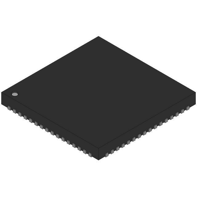
QFN 64−pin Package, 9 mm x 9 mm
Spread Spectrum Compatible: Tracks Input Clock Spreading for Low
EMI
0°C to +70°C Ambient Operating Temperature
These Devices are Pb−Free and are RoHS Compliant
© Semiconductor Components Industries, LLC, 2017
July, 2017 − Rev. 3
1
64
1
QFN64
MN SUFFIX
CASE 485DH
MARKING DIAGRAMS
1
1
NB3N
1200K
AWLYYWWG
NB3W
1200L
AWLYYWWG
NB3x1200x= Specific Device Code
A
= Assembly Location
WL
= Wafer Lot
YY
= Year
WW
= Work Week
G
= Pb−Free Package
ORDERING INFORMATION
Package
Shipping†
NB3N1200KMNG
QFN−64
(Pb−Free)
260 Units /
Tray
NB3N1200KMNTXG
QFN−64
(Pb−Free)
1000 / Tape &
Reel
NB3W1200LMNG
QFN−64
(Pb−Free)
260 Units /
Tray
NB3W1200LMNTXG
QFN−64
(Pb−Free)
1000 / Tape &
Reel
Device
†For information on tape and reel specifications,
including part orientation and tape sizes, please
refer to our Tape and Reel Packaging Specification
Brochure, BRD8011/D.
Publication Order Number:
NB3N1200K/D
�NB3N1200K, NB3W1200L
12
OE_[11:0]#
FB_OUT*
FB_OUT#*
SSC Compatible
PLL
CLK_IN
DIF_[11:0]
MUX
DIF_[11:0]#
CLK_IN#
100M_133M#
HBW_BYPASS_LBW#
SA_0
SA_1
PWRGD/PWRDN#
SDA
SCL
Control
Logic
* FB_OUT pins are for NB3N1200K only; they are NC for NB3W1200L
** IREF pin is for NB3N1200K only; it is NC for NB3W1200L
Figure 1. Simplified Block Diagram
www.onsemi.com
2
IREF**
RREF
�NB3N1200K, NB3W1200L
DIF_11#
DIF_11
OE_11#
OE_10#
DIF_10#
DIF_10
GND
VDD
VDD
DIF_9#
DIF_9
OE_9#
OE_8#
DIF_8#
DIF_8
VDD
PIN CONNECTIONS
64 63 62 61 60 59 58 57 56 55 54 53 52 51 50 49
VDDA
GNDA
IREF
100M_133M#
HBW_BYPASS_LBW#
PWRGD/PWRDN#
GND
VDDR
CLK_IN
CLK_IN#
SA_0
SDA
SCL
SA_1
FB_OUT#
FB_OUT
1
48
2
47
3
Exposed Pad (EP)
46
4
45
5
44
6
43
7
42
8
9
NB3N1200K
41
40
10
39
11
38
12
37
13
36
14
(Top View)
35
34
15
33
16
GND
DIF_7#
DIF_7
OE_7#
OE_6#
DIF_6#
DIF_6
GND
VDD
DIF_5#
DIF_5
OE_5#
OE_4#
DIF_4#
DIF_4
GND
DIF_0
DIF_0#
OE_0#
OE_1#
DIF_1
DIF_1#
GND
VDD
VDD
DIF_2
DIF_2#
OE_2#
OE_3#
DIF_3
DIF_3#
VDD
17 18 19 20 21 22 23 24 25 26 27 28 29 30 31 32
DIF_11#
DIF_11
OE_11#
OE_10#
DIF_10#
DIF_10
GND
VDD
VDD_IO
DIF_9#
DIF_9
OE_9#
OE_8#
DIF_8#
DIF_8
VDD_IO
Figure 2. NB3N1200K Pinout: QFN−64 (Top View)
64 63 62 61 60 59 58 57 56 55 54 53 52 51 50 49
1
48
2
47
3
Exposed Pad (EP)
46
4
45
5
44
6
43
7
42
8
9
NB3W1200L
41
40
10
39
11
38
12
37
13
36
14
(Top View)
35
34
15
33
16
17 18 19 20 21 22 23 24 25 26 27 28 29 30 31 32
DIF_0
DIF_0#
OE_0#
OE_1#
DIF_1
DIF_1#
GND
VDD
VDD_IO
DIF_2
DIF_2#
OE_2#
OE_3#
DIF_3
DIF_3#
VDD_IO
VDDA
GNDA
NC
100M_133M#
HBW_BYPASS_LBW#
PWRGD/PWRDN#
GND
VDDR
CLK_IN
CLK_IN#
SA_0
SDA
SCL
SA_1
NC
NC
Figure 3. NB3W1200L Pinout: QFN−64 (Top View)
www.onsemi.com
3
GND
DIF_7#
DIF_7
OE_7#
OE_6#
DIF_6#
DIF_6
GND
VDD
DIF_5#
DIF_5
OE_5#
OE_4#
DIF_4#
DIF_4
GND
�NB3N1200K, NB3W1200L
Table 1. NB3N1200K PIN DESCRIPTIONS
Pin Number
Pin Name
Type
Description
1
VDDA
3.3 V
3.3 V Power Supply for PLL.
2
GNDA
GND
Ground for PLL.
3
IREF
I
4
100M_133M#
I, SE
Input/output Frequency Selection (FS). An external pull−up
or pull−down resistor is attached to this pin to select the input/output frequency.
High = 100 MHz Output
Low = 133 MHz Output
5
HBW_BYPASS_LBW#
I, SE
Tri−Level input for selecting the PLL bandwidth or bypass mode
(refer to tri− level threshold in Table 4).
High = High BW mode Med = Bypass mode Low = Low BW mode
6
PWRGD / PWRDN#
I, SE
3.3 V LVTTL input to power up or power down the device.
7
GND
GND
Ground for outputs.
8
VDDR
VDD
3.3 V power supply for receiver.
A precision resistor is attached to this pin to set the differential output current.
Use RREF = 475 W, 1% for 100 Ohms trace.
Use RREF = 412 W, 1% for 85 Ohms trace.
9
CLK_IN
I, DIF
0.7 V Differential True input
10
CLK_IN#
I, DIF
0.7 V Differential Complementary input
11
SA_0
I, SE
3.3 V LVTTL input selecting the address.
Tri−level input (refer to tri−level threshold in Table 4.)
12
SDA
I/O
Open collector SMBus data.
13
SCL
I/O
SMBus slave clock input.
14
SA_1
I, SE
15
FB_OUT#
O, DIF
Complementary Feedback out pin, termination required.
See External Feedback Termination section.
16
FB_OUT
O, DIF
True Feedback out pin, termination required.
See External Feedback Termination section.
17
DIF_0
O, DIF
0.7 V Differential True clock output
18
DIF_0#
O, DIF
0.7 V Differential Complementary clock output
19
OE_0#
I, SE
3.3 V LVTTL active low input for enabling DIF output pair 0.
0 enables outputs, 1 disables outputs. Internal pull down.
20
OE_1#
I, SE
3.3 V LVTTL active low input for enabling DIF output pair 1.
0 enables outputs, 1 disables outputs. Internal pull down.
21
DIF_1
O, DIF
0.7 V Differential True clock output
22
DIF_1#
O, DIF
0.7 V Differential Complementary clock output
23
GND
GND
Ground for outputs.
24
VDD
3.3 V
3.3 V power supply for outputs.
25
VDD
3.3 V
3.3 V power supply for outputs.
26
DIF_2
O, DIF
0.7 V Differential True clock output
27
DIF_2#
O, DIF
0.7 V Differential Complementary clock output
28
OE_2#
I, SE
3.3 V LVTTL active low input for enabling DIF output pair 2.
0 enables outputs, 1 disables outputs. Internal pull down.
29
OE_3#
I, SE
3.3 V LVTTL active low input for enabling DIF output pair 3.
0 enables outputs, 1 disables outputs. Internal pull down.
30
DIF_3
O, DIF
0.7 V Differential True clock output
31
DIF_3#
O, DIF
0.7 V Differential Complementary clock output
32
VDD
3.3 V
3.3 V power supply for outputs.
33
GND
GND
Ground for outputs.
3.3 V LVTTL input selecting the address.
Tri−level input (refer to tri−level threshold in Table 4.)
www.onsemi.com
4
�NB3N1200K, NB3W1200L
Table 1. NB3N1200K PIN DESCRIPTIONS
Pin Number
Pin Name
Type
Description
34
DIF_4
O, DIF
0.7 V Differential True clock output
35
DIF_4#
O, DIF
0.7 V Differential Complementary clock output
36
OE_4#
I, SE
3.3 V LVTTL active low input for enabling DIF output pair 4.
0 enables outputs, 1 disables outputs. Internal pull down.
37
OE_5#
I, SE
3.3 V LVTTL active low input for enabling DIF output pair 5.
0 enables outputs, 1 disables outputs. Internal pull down.
38
DIF_5
O, DIF
0.7 V Differential True clock output
39
DIF_5#
O, DIF
0.7 V Differential Complementary clock output
40
VDD
3.3 V
3.3 V power supply for outputs.
41
GND
GND
Ground for outputs.
42
DIF_6
O, DIF
0.7 V Differential True clock output
43
DIF_6#
O, DIF
0.7 V Differential Complementary clock output
44
OE_6#
I, SE
3.3 V LVTTL active low input for enabling DIF output pair 6.
0 enables outputs, 1 disables outputs. Internal pull down.
45
OE_7#
I, SE
3.3 V LVTTL active low input for enabling DIF output pair 7.
0 enables outputs, 1 disables outputs. Internal pull down.
46
DIF_7
O, DIF
47
DIF_7#
O, DIF
48
GND
GND
Ground for outputs.
49
VDD
3.3 V
3.3 V power supply for outputs.
50
DIF_8
O, DIF
0.7 V Differential True clock output
51
DIF_8#
O, DIF
0.7 V Differential Complementary clock output
52
OE_8#
I, SE
3.3 V LVTTL active low input for enabling DIF output pair 8.
0 enables outputs, 1 disables outputs. Internal pull down.
53
OE_9#
I, SE
3.3 V LVTTL active low input for enabling DIF output pair 9.
0 enables outputs, 1 disables outputs. Internal pull down.
54
DIF_9
O, DIF
0.7 V Differential True clock output
55
DIF_9#
O, DIF
0.7 V Differential Complementary clock output
56
VDD
3.3 V
3.3 V power supply for outputs.
57
VDD
3.3 V
3.3 V power supply for outputs.
Ground for outputs.
0.7 V Differential True clock output
0.7 V Differential Complementary clock output
58
GND
GND
59
DIF_10
O, DIF
0.7 V Differential True clock output
60
DIF_10#
O, DIF
0.7 V Differential Complementary clock output
61
OE_10#
I, SE
3.3 V LVTTL active low input for enabling DIF output pair 10.
0 enables outputs, 1 disables outputs. Internal pull down.
62
OE_11#
I, SE
3.3 V LVTTL active low input for enabling DIF output pair 11.
0 enables outputs, 1 disables outputs. Internal pull down.
63
DIF_11
O, DIF
0.7 V Differential True clock output
64
DIF_11#
O, DIF
0.7 V Differential Complementary clock output
EP
Exposed Pad
Thermal
The Exposed Pad (EP) on the QFN−64 package bottom is thermally connected
to the die for improved heat transfer out of package. The exposed pad must be
attached to a heat−sinking conduit. The pad is electrically connected to the die,
and must be electrically and thermally connected to GND on the PC board.
www.onsemi.com
5
�NB3N1200K, NB3W1200L
Table 2. NB3W1200L PIN DESCRIPTIONS
Pin Number
Pin Name
Type
Description
1
VDDA
3.3 V
3.3 V Power Supply for PLL.
2
GNDA
GND
Ground for PLL.
3
NC
I/O
4
100M_133M#
I, SE
3.3 V tolerant inputs for input/output Frequency Selection (FS). An external pull−
up or
pull−down resistor is attached to this pin to select the input/output frequency.
High = 100 MHz Output
Low = 133 MHz Output
5
HBW_BYPASS_LBW#
I, SE
Tri−Level input for selecting the PLL bandwidth or bypass mode
(refer to tri− level threshold in Table 4).
High = High BW mode, Med = Bypass mode,
Low = Low BW mode
6
PWRGD / PWRDN#
I
7
GND
GND
Ground for outputs.
8
VDDR
VDD
3.3 V power supply for receiver.
No Connect
3.3 V LVTTL input to power up or power down the device.
9
CLK_IN
I, DIF
0.7 V Differential True input
10
CLK_IN#
I, DIF
0.7 V Differential Complementary input
11
SA_0
I
12
SDA
I/O
Open collector SMBus data.
13
SCL
I/O
SMBus slave clock input.
14
SA_1
I
15
NC
I/O
No Connect. There are active signals on pin 15;
do not connect anything to this pin.
16
NC
I/O
No Connect. There are active signals on pin 16;
do not connect anything to this pin.
17
DIF_0
O, DIF
0.7 V Differential True clock output
18
DIF_0#
O, DIF
0.7 V Differential Complementary clock output
19
OE_0#
I, SE
3.3 V LVTTL active low input for enabling DIF output pair 0.
0 enables outputs, 1 disables outputs. Internal pull down.
20
OE_1#
I, SE
3.3 V LVTTL active low input for enabling DIF output pair 1.
0 enables outputs, 1 disables outputs. Internal pull down.
21
DIF_1
O, DIF
0.7 V Differential True clock output
22
DIF_1#
O, DIF
0.7 V Differential Complementary clock output
23
GND
GND
24
VDD
3.3 V
3.3 V power supply for core.
25
VDD_IO
VDD
Power supply for differential outputs.
26
DIF_2
O, DIF
0.7 V Differential True clock output
27
DIF_2#
O, DIF
0.7 V Differential Complementary clock output
28
OE_2#
I, SE
3.3 V LVTTL active low input for enabling DIF output pair 2.
0 enables outputs, 1 disables outputs. Internal pull down.
29
OE_3#
I, SE
3.3 V LVTTL active low input for enabling DIF output pair 3.
0 enables outputs, 1 disables outputs. Internal pull down.
30
DIF_3
O, DIF
0.7 V Differential True clock output
31
DIF_3#
O, DIF
0.7 V Differential Complementary clock output
32
VDD_IO
VDD
Power supply for differential outputs.
33
GND
GND
Ground for outputs.
3.3 V LVTTL input selecting the address.
Tri−level input (refer to tri−level threshold in Table 4.)
3.3 V LVTTL input selecting the address. Tri−level input
(refer to tri−level threshold in Table 4.)
Ground for outputs.
www.onsemi.com
6
�NB3N1200K, NB3W1200L
Table 2. NB3W1200L PIN DESCRIPTIONS
Pin Number
Pin Name
Type
Description
34
DIF_4
O, DIF
0.7 V Differential True clock output
35
DIF_4#
O, DIF
0.7 V Differential Complementary clock output
36
OE_4#
I, SE
3.3 V LVTTL active low input for enabling DIF output pair 4.
0 enables outputs, 1 disables outputs. Internal pull down.
37
OE_5#
I, SE
3.3 V LVTTL active low input for enabling DIF output pair 5.
0 enables outputs, 1 disables outputs. Internal pull down.
38
DIF_5
O, DIF
0.7 V Differential True clock output
39
DIF_5#
O, DIF
0.7 V Differential Complementary clock output
40
VDD
3.3 V
3.3 V power supply for core.
41
GND
GND
Ground for outputs.
42
DIF_6
O, DIF
0.7 V Differential True clock output
43
DIF_6#
O, DIF
0.7 V Differential Complementary clock output
44
OE_6#
I, SE
3.3 V LVTTL active low input for enabling DIF output pair 6.
0 enables outputs, 1 disables outputs. Internal pull down.
45
OE_7#
I, SE
3.3 V LVTTL active low input for enabling DIF output pair 7.
0 enables outputs, 1 disables outputs. Internal pull down.
46
DIF_7
O, DIF
47
DIF_7#
O, DIF
48
GND
GND
Ground for outputs.
49
VDD_IO
VDD
Power supply for differential outputs.
50
DIF_8
O, DIF
0.7 V Differential True clock output
51
DIF_8#
O, DIF
0.7 V Differential Complementary clock output
52
OE_8#
I, SE
3.3 V LVTTL active low input for enabling DIF output pair 8.
0 enables outputs, 1 disables outputs. Internal pull down.
53
OE_9#
I, SE
3.3 V LVTTL active low input for enabling DIF output pair 9.
0 enables outputs, 1 disables outputs. Internal pull down.
54
DIF_9
O, DIF
0.7 V Differential True clock output
55
DIF_9#
O, DIF
0.7 V Differential Complementary clock output
56
VDD_IO
VDD
Power supply for differential outputs.
57
VDD
3.3 V
3.3 V power supply for core.
Ground for outputs.
0.7 V Differential True clock output
0.7 V Differential Complementary clock output
58
GND
GND
59
DIF_10
O, DIF
0.7 V Differential True clock output
60
DIF_10#
O, DIF
0.7 V Differential Complementary clock output
61
OE_10#
I, SE
3.3 V LVTTL active low input for enabling DIF output pair 10.
0 enables outputs, 1 disables outputs. Internal pull down.
62
OE_11#
I, SE
3.3 V LVTTL active low input for enabling DIF output pair 11.
0 enables outputs, 1 disables outputs. Internal pull down.
63
DIF_11
O, DIF
0.7 V Differential True clock output
64
DIF_11#
O, DIF
0.7 V Differential Complementary clock output
EP
Exposed Pad
Thermal
The Exposed Pad (EP) on the QFN−64 package bottom is thermally connected
to the die for improved heat transfer out of package. The exposed pad must be
attached to a heat−sinking conduit. The pad is electrically connected to the die,
and must be electrically and thermally connected to GND on the PC board.
www.onsemi.com
7
�NB3N1200K, NB3W1200L
Table 3. MAXIMUM RATINGS
Symbol
Parameter
VDD/VDDA/VDDR
VDD_IO
Condition
Min
Max
Units
Core Supply Voltage
4.6
V
I/O Supply Voltage
4.6
V
4.6
V
5.5
V
VIH (Note 1)
Input High Voltage
VIHSMB
SMB Input High Voltage
VIL
3.3 V Input Low Voltage
−0.5
ts
Storage Temperature
−65
ESD prot.
Input ESD protection
Human Body Model
qJA
Thermal Resistance
(Junction−to−Ambient)
0 lfpm
500 lfpm
IOUTmax
Maximum Output Current
SDA, SCL Pins
NB3N1200K
NB3W1200L
V
150
°C
22
15
°C/W
24
12
mA
2000
V
Powerdown Mode
(PWRGD/PWRDN# = 0)
All Pairs Tri−stated
All Pairs Tri−state Low/Low
Stresses exceeding those listed in the Maximum Ratings table may damage the device. If any of these limits are exceeded, device functionality
should not be assumed, damage may occur and reliability may be affected.
1. Maximum VIH is not to exceed maximum VDD.
Table 4. DC OPERATING CHARACTERISTICS (VDD = VDDA = VDDR = 3.3 V ±5%, TA = 0°C − 70°C)
Symbol
Parameter
Condition
Min
Max
Units
VDD/VDDA/VDDR
3.3 V Core Supply Voltage
3.3 V ±5%
3.135
3.465
V
1.05 V to 3.3 V ±5%
0.975
3.465
V
330
180
mA
6
6
mA
5.5
V
VDD_IO (Note 2)
IDD
IDDPD
I/O Supply Voltage
Power Supply Current
NB3N1200K
NB3W1200L
At 133 MHz, CL = 2 pF
Power Down Current
NB3N1200K
NB3W1200L
VIH (Note 3)
Input High Voltage, Single−Ended Inputs
2.0
VIL (Note 3)
Input Low Voltage, Single−Ended Inputs
GND−0.3
0.8
V
VIHCLK_IN
CLK_IN/CLK_IN# High
600
1150
mV
VILCLK_IN
CLK_IN/CLK_IN# Low
−300
300
mV
IIL (Note 4)
Input Leakage Current
−5
+5
mA
VIH_FS (Note 5)
Input High Voltage
0.7
VDD+0.3
V
VIL_FS (Note 5)
Input Low Voltage
GND−0.3
0.35
V
VIL_Tri (Note 6)
Tri−Level Input Low Voltage
0
0.8
V
VIM_Tri (Note 6)
Tri−Level Input Med Voltage
1.2
1.8
V
VIH_Tri (Note 6)
Tri−Level Input High Voltage
2.2
VDD
V
VOH (Note 7)
Output High Voltage SCL, SDA
IOH = −1 mA
VOL (Note 7)
Output Low Voltage SCL, SDA
IOL = 1 mA
Cin (Note 8)
Input Capacitance
Cout (Note 8)
Output Capacitance
2.
3.
4.
5.
6.
7.
8.
Lpin
Pin Inductance
ta
Ambient Temperature
0 < VIN < VDD
No Airflow
0.4
V
2.5
4.5
pF
2.5
4.5
pF
7
nH
0
70
°C
VDD_IO applies to the low power NMOS push−pull NB3W1200L only.
SDA, SCL, OEn#, PWRGD/PWRDN#.
Input Leakage Current does not include inputs with pull−up or pull−down resistors.
100M_133M# Frequency Select (FS).
SA_0, SA_1, HBW_BYPASS_LBW#.
Signal edge is required to be monotonic when transitioning through this region.
Ccomp capacitance based on pad metallization and silicon device capacitance. Not including package pin capacitance.
www.onsemi.com
8
V
2.4
�NB3N1200K, NB3W1200L
NB3N1200K / NB3W1200L Output Relational Timing Parameters
Table 5. ELECTRICAL CHARACTERISTICS − Skew and Differential Jitter Parameters
(VDD = VDDA = VDDR = 3.3 V ±5%, TA = 0 − 70°C)
Group
CLK_IN, DIF[x:0]
(Notes 9, 10, 12, 13)
Description
Min
Input−to−Output Delay in PLL mode, nominal value
Typ
Max
Units
−100
100
ps
2.5
4.5
ns
CLK_IN, DIF[x:0]
(Notes 10, 11, 13)
Input−to−Output Delay in Bypass mode, nominal value
CLK_IN, DIF[x:0]
(Notes 10, 11, 13)
Input−to−Output Delay variation in PLL mode
(over voltage and temperature), nominal value
|100|
ps
CLK_IN, DIF[x:0]
(Notes 10, 11, 13)
Input−to−Output Delay variation in Bypass mode
(over voltage and temperature), nominal value
|250|
ps
50
ps
DIF[11:0]
(Notes 9, 10, 11, 13)
Output−to−Output Skew across all 12 outputs
(Common to Bypass and PLL mode)
0
9. Measured into fixed 2 pF load capacitance. Input to output skew is measured at the first output edge following the corresponding input.
10. Measured from differential cross−point to differential cross−point.
11. All Bypass Mode Input−to−Output specs refer to the timing between an input edge and the specific output edge created by it.
12. This parameter is deterministic for a given device.
13. Measured with scope averaging on to find mean value.
www.onsemi.com
9
�NB3N1200K, NB3W1200L
Table 6. LOW BAND PHASE JITTER − PLL MODE
Group
Typ
Max
Units
Output PCIe Gen1
13
86
ps
(p−p)
DIF
(Notes 14, 15, 17, 19)
Output PCIe Gen2 Low Band, 10 kHz < f < 1.5 MHz
0.1
3.0
ps
RMS
DIF
(Notes 14, 15, 17, 19)
Output PCIe Gen2 High Band, 1.5 MHz < f < 50 MHz
0.8
3.1
ps
RMS
DIF
(Notes 14, 16, 17)
Parameter
Min
HIGH BAND, 1.5 MHz < F < Nyquist
DIF
(Notes 14, 15, 17, 19)
Output phase jitter impact – PCIe* Gen3
(including PLL BW 2 – 4 MHz, CDR = 10 MHz)
0.18
1.0
ps
RMS
DIF
(Notes 14, 15, 17, 19)
Output phase jitter impact – PCIe* Gen4
(including PLL BW 2 – 4 MHz, CDR = 10 MHz)
0.18
0.5
ps
RMS
Output Intel UPI intermediate frequency accumulated jitter
(9.6 Gb/s, 10.4 Gb/s or 11.2 Gb/s, 100 MHz, 12 UI)
0.5
1.0
ps
RMS
DIF
(Notes 14, 18, 20)
Output Intel QPI & Intel SMI REFCLK accumulated jitter
(4.8 Gb/s or 6.4 Gb/s, 100 MHz or 133 MHz, 12 UI)
0.14
0.5
ps
RMS
DIF
(Notes 14, 18)
Output Intel QPI & Intel SMI REFCLK accumulated jitter
(8 Gb/s, 100 MHz, 12 UI)
0.07
0.3
ps
RMS
DIF
(Notes 14, 18)
Output Intel QPI & Intel SMI REFCLK accumulated jitter
(9.6 Gb/s, 100 MHz, 12 UI)
0.06
0.2
ps
RMS
Typ
Max
Units
Output PCIe Gen1
0.04
10
ps
(p−p)
DIF
(Notes 14, 15, 17, 19)
Output PCIe Gen2 Low Band, 10 kHz < f < 1.5 MHz
0.001
0.3
ps
RMS
DIF
(Notes 14, 15, 17, 19)
Output PCIe Gen2 High Band, 1.5 MHz < f < 50 MHz
0.002
0.7
ps
RMS
DIF
(Notes 14, 15, 17, 19)
Output phase jitter impact – PCIe* Gen3
0.001
0.3
ps
RMS
DIF
(Notes 14, 15, 17, 19)
Output phase jitter impact – PCIe* Gen4
0.001
0.3
ps
RMS
DIF
(Notes 14, 18, 20)
Output Intel QPI & Intel SMI REFCLK accumulated jitter
(4.8 Gb/s or 6.4 Gb/s, 100 MHz or 133 MHz, 12 UI)
0.001
0.3
ps
RMS
DIF
(Notes 14, 18)
Output Intel QPI & Intel SMI REFCLK accumulated jitter
(8 Gb/s, 100 MHz, 12 UI)
0.001
0.1
ps
RMS
DIF
(Notes 14, 18)
Output Intel QPI & Intel SMI REFCLK accumulated jitter
(9.6 Gb/s, 100 MHz, 12 UI)
0.001
0.1
ps
RMS
DIF
(Notes 14, 18)
Table 7. ADDITIVE PHASE JITTER − BYPASS MODE
Group
DIF
(Notes 14, 16, 17)
Parameter
Min
14. Post processed evaluation through Intel supplied Matlab scripts. Tested with NB3N1200K/NB3W1200L driven by a CK420BQ or equivalent.
15. PCIe Gen4 filter characteristics are subject to final ratification by PCISIG. Please check the PCI SIG for the latest specification.
16. These jitter numbers are defined for a BER of 1E−12. Measured numbers at a smaller sample size have to be extrapolated to this BER target.
17. ⎛ = 0.54 is implying a jitter peaking of 3 dB.
18. Measuring on 100 MHz output using Intel supplied clock template jitter tool.
19. Measuring on 100 MHz PCIe SRC output using Intel supplied clock jitter tool.
20. Measuring on 100 MHz, 133 MHz output using Intel supplied clock jitter tool.
Table 8. PLL BANDWIDTH AND PEAKING
Group
Parameter
Min
Typ
Max
Units
DIF (Note 21)
PLL Jitter Peaking (HBW_BYPASS_LBW# = 0)
−
0.7
2.0
dB
DIF (Note 21)
PLL Jitter Peaking (HBW_BYPASS_LBW# = 1)
−
0.4
2.5
dB
DIF (Note 22)
PLL Bandwidth (HBW_BYPASS_LBW# = 1)
2.0
2.7
4.0
MHz
DIF (Note 22)
PLL Bandwidth (HBW_BYPASS_LBW# = 0)
0.7
0.9
1.4
MHz
21. Measured as maximum pass band gain. At frequencies within the loop BW, highest point of magnification is called PLL jitter peaking.
22. Measured at 3 db down or half power point.
www.onsemi.com
10
�NB3N1200K, NB3W1200L
Table 9. DIF 0.7 V AC TIMING CHARACTERISTICS (Non−Spread or −0.5% Spread Spectrum Mode)
(VDD = VDDA = VDDR = 3.3 V ±5%)
CLK = 100 MHz, 133.33 MHz
Min
Symbol
Parameter
Tstab (Note 44)
Clock Stabilization Time
Laccuracy (Notes 26, 30, 38, 45)
Tabs (Notes 26, 27, 30)
Long Accuracy
Absolute
Min/Max
Host CLK
Period
No Spread
−0.5% Spread
Slew_rate (Notes 24, 26, 30)
DIFF OUT Slew_rate (see Figure 4)
DTrise / DTfall (Notes 26, 29, 40)
Rise and Fall Time Variation
9.94900 for 100 MHz
Max
Unit
1.8
ms
100
ppm
10.05100 for 100 MHz
ns
7.44925 for 133 MHz
7.55075 for 133 MHz
9.49900 for 100 MHz
10.10126 for 100 MHz
7.44925 for 133 MHz
7.58845 for 133 MHz
1.0
Rise/Fall Matching (Notes 26, 30, 41, 43)
4.0
V/ns
125
ps
20
%
VHigh (Notes 26, 29, 32)
Voltage High (typ 0.70 Volts)
660
850
mV
VLow (Notes 26, 29, 33)
Voltage Low (typ 0.0 Volts)
−150
150
mV
Vmax (Note 29)
Maximum Voltage
1150
mV
Vcross absolute (Notes 23, 25, 26, 29, 36)
Absolute Crossing Point Voltages
250
550
mV
Vcross relative (Notes 26, 28, 29, 36)
Relative Crossing Point Voltages
Calc
Calc
Total D Vcross (Notes 26, 29, 37)
Total Variation of Vcross
Over All Edges
140
mV
Tccjitter (Notes 26, 30, 42)
Cycle−to−Cycle Jitter
50
ps
Duty Cycle (Notes 26, 30)
PLL and Bypass Modes
45
55
%
tOE# Latency
OE# Latency − DIFF start after OE#
Assertion
− DIFF stop after OE# Deassertion
4
12
Clocks
Vovs (Notes 26, 29, 34)
Maximum Voltage (Overshoot)
Vhigh + 0.3
V
Vuds (Notes 26, 29, 35)
Maximum Voltage (Undershoot)
Vlow − 0.3
V
Vrb (Notes 26, 29)
Ringback Voltage
N/A
V
0.2
23. Measured at crossing point where the instantaneous voltage value of the rising edge of CLK equals the falling edge of CLK#.
24. Measurment taken from differential waveform on a component test board. The slew rate is measured from −150 mV to +150 mV on the
differential waveform. Scope is set to average because the scope sample clock is making most of the dynamic wiggles along the clock edge
Only valid for Rising CLK_IN and Falling CLK_IN#. Signal must be monotonic through the Vol to Voh region for Trise and Tfall.
25. This measurement refers to the total variation from the lowest crossing point to the highest, regardless of which edge is crossing.
26. Test configuration is Rs = 33.2 W, Rp = 49.9, 2 pF for 100 W transmission line; Rs = 27 W, Rp = 42.2, 2 pF for 85 W transmission line.
27. The average period over any 1 ms period of time must be greater than the minimum and less than the maximum specified period.
28. Vcross(rel) Min and Max are derived using the following, Vcross(rel) Min = 0.250 + 0.5 (Vhavg − 0.700), Vcross(rel) Max = 0.550 − 0.5 (0.700
– Vhavg), (see Figure 7).
29. Measurement taken from Single Ended waveform.
30. Measurement taken from differential waveform. Bypass mode, input duty cycle = 50%.
31. Unless otherwise noted, all specifications in this table apply to all processor frequencies.
32. VHigh is defined as the statistical average High value as obtained by using the Oscilloscope VHigh Math function.
33. VLow is defined as the statistical average Low value as obtained by using the Oscilloscope VLow Math function.
34. Overshoot is defined as the absolute value of the maximum voltage.
35. Undershoot is defined as the absolute value of the minimum voltage.
36. The crossing point must meet the absolute and relative crossing point specifications simultaneously.
37. DVcross is defined as the total variation of all crossing voltages of Rising DIFF and Falling DIFF#. This is the maximum allowed variance
in Vcross for any particular system.
38. Using frequency counter with the measurement interval equal or greater than 0.15 s, target frequencies are 100,000,000 Hz, 133,333,333 Hz.
39. Using frequency counter with the measurement interval equal or greater than 0.15 s, target frequencies are 99,750,00 Hz, 133,000,000 Hz.
40. Measured with oscilloscope, averaging off, using min max statistics. Variation is the delta between min and max.
41. Measured with oscilloscope, averaging on, The difference between the rising edge rate (average) of DIFF versus the falling edge rate
(average) of DIFF#. Measured in a ±75 mV window around the crosspoint of DIFF and DIFF#.
42. Measured with device in PLL mode, in BYPASS mode jitter is additive.
43. Rise/Fall matching is derived using the following, 2*(Trise – Tfall) / (Trise + Tfall).
44. This is the time from the valid CLK_IN input clocks and the assertion of the PWRGD signal level at 1.8 V – 2.0 V to the time that stable clocks
are output from the buffer chip (PLL locked).
45. All Long Term Accuracy specifications are guaranteed with the assumption that the input clock complies with CK410B+/CK420BQ accuracy
requirements. The NB3N1200K and NB3W1200L itself do not contribute to ppm error.
www.onsemi.com
11
�NB3N1200K, NB3W1200L
Table 10. CLOCK PERIOD SSC DISABLED
Measurement Window
SSC OFF
Center
Freq.
MHz
1 Clock
1 ms
0.1 s
0.1 s
0.1 s
1 ms
1 Clock
− Jitter c−c
Abs Per Min
− SSC Short
Avg Min
− ppm Long
Avg Min
0 ppm
Period
+ ppm Long
Avg Max
+ SSC Short
Avg Max
+ Jitter c−c
Abs Per Max
Units
100.00
9.94900
9.99900
10.00000
10.00100
10.05100
ns
133.33
7.44925
7.49925
7.50000
7.50075
7.55075
ns
Table 11. CLOCK PERIOD SSC ENABLED
Measurement Window
SSC ON
Center
Freq.
MHz
1 Clock
1 ms
0.1 s
0.1 s
0.1 s
1 ms
1 Clock
− Jitter c−c
Abs Per Min
− SSC Short
Avg Min
− ppm Long
Avg Min
0 ppm
Period
+ ppm Long
Avg Max
+ SSC Short
Avg Max
+ Jitter c−c
Abs Per Max
Units
99.75
9.94900
9.99900
10.02406
10.02506
10.02607
10.05126
10.10126
ns
133.00
7.44925
7.49925
7.51805
7.51880
7.51955
7.53845
7.58845
ns
Table 12. INPUT EDGE RATE (Note 46)
Frequency Select (FS)
Min
Max
Unit
100 MHz
0.35
N/A
V/ns
133 MHz
0.35
N/A
V/ns
46. Input edge rate is based on single ended measurement. This is the minimum input edge rate at which the NB3N1200K / NB3W1200L devices
are guaranteed to meet all performance specifications.
www.onsemi.com
12
�NB3N1200K, NB3W1200L
Measurement Points for Differential
DIFFX#
Trise (DIFFX)
VOH = 0.525 V
VCross
VOL = 0.175 V
DIFFX
Tfall (DIFFX#)
Figure 4. Single−Ended Measurement Points for Trise, Tfall
Vovs
VHigh
Vrb
Vrb
VLow
Vuds
Figure 5. Single−Ended Measurement Points for Vovs, Vuds, Vrb
TPeriod
High Duty Cycle%
Low Duty Cycle%
Skew measurement point
0.0 V
Figure 6. Differential (DIFFX – DIFFX#) Measurement Points (Tperiod, Duty Cycle, Jitter)
www.onsemi.com
13
�NB3N1200K, NB3W1200L
600
CLK_IN, CLK_IN#
Vcross(rel) Max
The differential input clock is expected to be sourced from
a clock synthesizer.
CROSSING POINT (mV)
550
500
OE# and Output Enables (Control Registers)
450
400
For
Vhigh < 700 mV
Use Equ. 1
Each output can be individually enabled or disabled by
SMBus control register bits. Additionally, each output of the
DIF[11:0] has a dedicated OE# pin. The OE# pins are
asynchronous asserted−low signals. The Output Enable bits
in the SMBus registers are active high and are set to enable
by default.
The disabled state for the NB3N1200K HCSL outputs is
Hi−Z, with the termination network pulling the outputs
Low/Low. The disabled state for the NB3W1200L low
power NMOS Push−Pull outputs is Low/Low. In the
following text, if the NB3N1200K HCSL output is referred
to as Hi−Z or Tri− state, the equivalent state of the
NB3W1200L NMOS Push−pull output is Low/Low.
Please note that the logic level for assertion or deassertion
is different in software than it is on hardware. This follows
hardware default nomenclature for communication
channels (e.g., output is enabled if OE# pin is pulled low)
and still maintains software programming logic (e.g., output
is enabled if OE register is true).
Please refer to Table 13 for the truth table for enabling and
disabling outputs via hardware and software. Note that both
the control register bit must be a ‘1’ AND the OE# pin must
be a ‘0’ for the output to be active.
NOTE: The assertion and de−assertion of this signal is
absolutely asynchronous.
For
Vhigh > 700 mV
Use Equ. 2
350
300
Vcross(rel) Min
250
200
625 650 675
700
725
750
775
800
825 850
VHigh AVERAGE (mV)
Equ 1: Vcross(rel) Max = 0.550 − 0.5(0.7 − Vhavg)
Equ 2: Vcross(rel) Min = 0.250 + 0.5(Vhavg − 0.7)
Figure 7. Vcross Range Clarification
The picture above illustrates the effect of Vhigh above and
below 700 mV on the Vcross range. The purpose of this is
to prevent a 250 mV Vcross with an 850 mV Vhigh. In
addition, this prevents the case of a 550 mV Vcross with a
660 mV Vhigh. The actual specification for Vcross is
dependent upon the measured amplitude of Vhigh.
Table 13. NB3N1200K OE AND POWER MANAGEMENT
Inputs
OE# Hardware Pins & Control Register Bits
Outputs
PWRGD/
PWRDN#
CLK_IN/
CLK_IN#
SMBUS
Enable Bit
OE# Pin
DIF/DIF# [11:0]
FB_OUT/
FB_OUT#
PLL State
0
X
X
X
Hi−Z
Hi−Z
OFF
1
Running
0
X
Hi−Z
Running
ON
1
0
Running
Running
ON
1
1
Hi−Z
Running
ON
Table 14. NB3W1200L POWER MANAGEMENT
Inputs
PWRGD/
PWRDN#
OE# Hardware Pins & Control Register Bits
Outputs
CLK_IN/
CLK_IN#
SMBUS
Enable Bit
OE# Pin
DIF/DIF# [11:0]
NC pins
(Pins 15, 16)
PLL State
0
X
X
X
Low/Low
Low/Low
OFF
1
Running
0
X
Low/Low
Running
ON
1
0
Running
Running
ON
1
1
Low/Low
Running
ON
www.onsemi.com
14
�NB3N1200K, NB3W1200L
OE# Assertion (Transition from ‘1’ to ‘0’)
Table 16. SMBUS ADDRESS TABLE
All differential outputs that were tri−stated are to resume
normal operation in a glitch free manner. The latency from
the assertion to active outputs is 4 − 12 DIF clock periods.
SA_1
SA_0
SMBUS Address
L
L
D8
L
M
DA
L
H
DE
M
L
C2
M
M
C4
M
H
C6
H
L
CA
H
M
CC
H
H
CE
OE# De-Assertion (Transition from ‘0’ to ‘1’)
The impact of de−asserting OE# is each corresponding
output will transition from normal operation to tri−state in
a glitch free manner. A minimum of 4 valid clocks will be
provided after the de−assertion of OE#. The maximum
latency from the de−assertion to tri−stated outputs is 12 DIF
clock periods.
100M_133M# − Frequency Selection (FS)
The NB3N1200K / NB3W1200L is optimized for lowest
phase jitter performance at 100 MHz and 133 MHz
operating frequencies. The 100M_133M# is a hardware pin,
which programs the appropriate output frequency of the DIF
pairs. Note that the CLK_IN frequency is equal to
CLK_OUT frequency; this means that the NB3N1200K /
NB3W1200L is operated in the 1:1 mode only. The
Frequency Selection can be enabled by the 100M_133M#
hardware pin. An external pull−up or pull−down resistor is
attached to this pin to select the input/output frequency. The
functionality is summarized in Table 15.
PWRGD/PWRDN#
PWRGD/PWRDN# is a dual function pin. PWRGD is
asserted high and de−asserted low. De−assertion of PWRGD
(pulling the signal low) is equivalent to indicating a
powerdown condition. PWRGD (assertion) is used by the
NB3N1200K / NB3W1200L to sample initial
configurations such as frequency select condition and SA
selections.
After PWRGD has been asserted high for the first time,
the pin becomes a PWRDN# (Power Down) pin that can be
used to shut off all clocks cleanly and instruct the device to
invoke power savings mode. PWRDN# is a completely
asynchronous active low input. When entering power
savings mode, PWRDN# should be asserted low prior to
shutting off the input clock or power to ensure all clocks
shut down in a glitch free manner. When PWRDN# is
asserted low by two consecutive rising edges of DIF#, all
differential outputs are held tri−stated on the next DIF# high
to low transition. The assertion and de-assertion of
PWRDN# is absolutely asynchronous.
WARNING: Disabling of the CLK_IN input clock prior
to assertion of PWRDN# is an undefined
mode and not recommended. Operation in
this mode may result in glitches, excessive
frequency shifting, etc.
Table 15. FREQUENCY SELECT (FS) PROGRAM
100M_133M#
Optimized Frequency
(CLK_IN = CLK_OUT)
0
133.33 MHz
1
100.00 MHz
NOTE: All differential outputs transition from 100 MHz
to 133 MHz or from 133 MHz to 100 MHz in a
glitch free manner.
SA_0, SA_1 – Address Selection
SA_0 and SA_1 are tri−level hardware pins, which
program the appropriate address for the NB3N1200K /
NB3W1200L. The two tri-level input pins that can
configure the NB3N1200K / NB3W1200L to nine different
addresses (refer to Table 4 for VIL_Tri, VIM_Tri, VIH_Tri
signal level).
Table 17. PWRGD/PWRDN# FUNCTIONALITY
PWRGD/PWRDN#
DIF
DIF#
0
Tri−state
Tri−state
1
Running
Running
www.onsemi.com
15
�NB3N1200K, NB3W1200L
Buffer Power−Up State Machine
Table 18. BUFFER POWER−UP STATE MACHINE
State
Description
0
3.3 V Buffer power off
1
After 3.3 V supply is detected to rise above 3.135 V, the buffer enters State 1 and initiates a 0.1 ms–0.3 ms delay.
2
Buffer waits for a valid clock on the CLK input and PWRDN# de−assertion (or PWRGD assertion low to high)
3
Once the PLL is locked to the CLK_IN input clock, the buffer enters state 3 and enables outputs for normal operation.
(Notes 47, 48)
47. The total power up latency from power on to all outputs active must be less than 1.8 ms (assuming a valid clock is present on CLK_IN input).
48. If power is valid and powerdown is de−asserted (PWRGD asserted) but no input clocks are present on the CLK_IN input, DIF clocks must
remain disabled. Only after valid input clocks are detected, valid power, PWRDN# de−asserted (PWRGD asserted) with the PLL
locked/stable and the DIF outputs enabled.
No input clock
State 1
State 2
Delay
0.1 ms − 0.3 ms
Wait for input
clock and
powerdown
de−assertion
Powerdown Asserted
State 0
State 3
Power Off
Normal
Operation
Figure 8. Buffer Power−Up State Diagram
Device Power−Up Sequence
3. Apply power to the device.
4. Once the VDD pin has reached a valid VDDmin
level (3.3V −5%), the PWRGD/PWRDN# pin
must be asserted High. See Figure 9.
Note: If no clock is present on the CLK_IN/CLK_IN#
pins when device is powered up, there will be no clock on
DIF/DIF# outputs.
Follow the power−up sequence below for proper device
functionality:
1. PWRGD/PWRDN# pin must be Low.
2. Assign remaining control pins to their required
state (100M_133M#, HBW_BYPASS_LBW#,
SDA, SCL)
Figure 9. PWRGD and VDD Relationship Diagram
www.onsemi.com
16
�NB3N1200K, NB3W1200L
PWRDN# Assertion
When PWRDN# is sampled low by two consecutive rising edges of DIF#, all differential outputs must held tri-stated on the
next DIF# high to low transition.
PWRDN#
DIF
DIF#
Figure 10. PWRDN#—Assertion
PWRGD Assertion
The power−up latency is to be less than 1.8 ms. This is the
time from the valid CLK_IN input clocks and the assertion
of the PWRGD signal to the time that stable clocks are
output from the buffer chip (PLL locked). All differential
outputs stopped in a tri−state condition resulting from power
down must be driven high in less than 300 ms of PWRDN#
de−assertion to a voltage greater than 200 mV.
Tstable
0 and


 工商网监
湘ICP备2023018690号
工商网监
湘ICP备2023018690号
