NB3N502DEVB NB3N502 Evaluation Board User’s Manual
http://onsemi.com Description
The NB3N502 Evaluation Board was designed to provide a flexible and convenient platform to quickly evaluate, characterize and verify the performance and operation of the NB3N502 PLL Clock Multiplier. This user’s manual provides detailed information on the board’s contents, layout and use, and it should be used in conjunction with the NB3N502 data sheet which contains full technical details on device specifications and operation (www.onsemi.com).
Board Features
• Supports the Use of a 5 MHz to 27 MHz Through−hole • SMA Connectors are Provided for Auxiliary Input and • Incorporates Onboard Slide Switch Controlled
This Evaluation Board Manual Contains
or Surface Mount Crystal Output Interfaces
Multiplier Select Pins, Minimizing Excess Cabling Information on the NB3N502 Evaluation Board Appropriate Lab Setup Evaluation Board Layout Bill of Materials
• Fully Assembled Evaluation Board • Accommodates the Electrical Characterization of the
NB3N502 in the SOIC−8 Package
• • • •
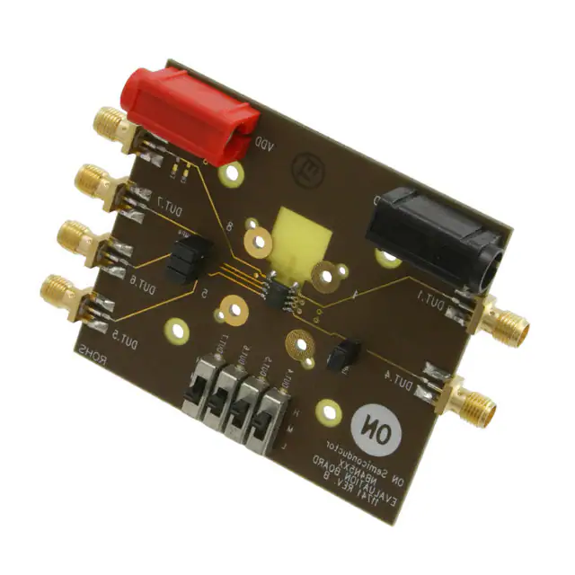
Figure 1. NB3N502 Evaluation Board
© Semiconductor Components Industries, LLC, 2006
October, 2006 − Rev. 0
1
Publication Order Number: NB3N502DEVB/D
�NB3N502DEVB
SETUP FOR MEASUREMENTS
Basic Equipment
• • • • • •
Signal Generator (for External Reference Clock Input) Oscilloscope Power Supply Voltmeter High−Speed Cables with SMA Connectors High−Impedance Probe
Power Supply Connections
External power supply of +3 V to +5.5 V must be provided to the board. The NB4N502 has a positive supply pin, VDD, and a ground pin, GND. Connect a single power supply to the evaluation board (see Figure 2.) by connecting VDD to the positive supply, +3 V to +5.5 V, and GND to 0 V. Power supply banana plug connectors for VDD and GND are provided at the top corners of the board.
Table 1. POWER SUPPLY CONNECTIONS
Supply VDD GND Value +3 to +5.5 V 0V Power Supplies Connector Red Banana Plug Black Banana Plug
mode crystal should be used. The evaluation board includes pads for small capacitors from X1/CLK to ground and from X2 to ground. These capacitors, CL1 and CL2, are used to adjust the stray capacitance of the board to match the nominally required crystal load capacitance (CLOAD (crystal)). Crystal load capacitors must be connected from each of the pins X1 and X2 to ground. The load capacitance of the crystal (CLOAD (crystal)) must be matched by total load capacitance of the oscillator circuitry network, CINX, CSX and CLX, as seen by the crystal (see Figure 3 and equations below). CLOAD1 = CIN1 + CS1 + CL1 [Total capacitance on X1/CLK] CLOAD2 = CIN2 + CS2 + CL2 [Total capacitance on X2] CIN1 [ CIN2 [ 12 pF (Typ) [Internal capacitance] CS1 [ CS2 [ 5 pF (Typ) [External PCB stray capacitance] CLOAD1,2 = 2 – CLOAD (Crystal) CL2 = CLOAD2 − CIN2 − CS2 [External load capacitance on X2] CL1 = CLOAD1 − CIN1 − CS1 [External load capacitance on X1/CLK]
Internal to Device
R G
+
−
CIN1 12pF GND X1/CLK CS1 CS2 X2
CIN2 12pF
VDD
CL1
CL2
+3.0 V to +5.5 V
Figure 2. Power Supply Connections External Reference Clock
Crystal
Figure 3. Using a Crystal as Reference Clock
An SMA connector is provided for X1/CLK if an external clock source is used on Pin 1. The metal trace at the package pin is intentionally open for crystal use and must be shorted for a connection to Pin 1 for external clock use.
Crystal and Crystal Load Capacitors Selection Guide
Control and Select Pins
A through−hole or surface mount crystal can be used. The metal traces at the crystal pins are intentionally open for crystal use and will have no impedance effect on the crystal pins. The total on−chip capacitance is approximately 12 pF per pin (CIN1 and CIN2). A parallel resonant, fundamental
The NB4N502 evaluation board is equipped with SMA connectors to control the static input logic levels of the Multiplier Select pins, S0 and S1 (see Table 2). Pin S1 defaults to M when left open. Pin S0 defaults to H when left open. 3−Position slide switches are also provided to control the Multiplier Select pins. To use the switches, headers JMP3 and JMP4 must be shorted.
http://onsemi.com
2
�NB3N502DEVB
1. Using the SMA Connectors a. SMA connectors J3 and J4 (DUT.6 and DUT.7) should be pulled to VCC for logic level HIGH, pulled to GND for logic level LOW, and left OPEN for logic level M. 2. Using the Slide Switches a. Header pins JMP3 and JMP4 enable the slide switches for the clock multiplier select lines, S0 and S1, and should be jumpered. b. Switches SW3 (DUT.6) and SW4 (DUT.7) are used to select the clock multiplier value (see Table 2). c. The H position of the slide switch asserts a logic HIGH on the assigned pin, the L asserts a logic LOW and the M is an open where the pin “floats” to a mid−logic level by way of the device’s internal pullup and pulldown resistors.
Table 2. CLOCK MULTIPLIER SELECT TABLE
S1* SW4 (DUT.7) L L M M H H S0** SW3 (DUT.6) L H L H L H Multiplier 2X 5X 3X 3.33X 4X 2.5X
L = GND, H = VDD, M = OPEN (unconnected) *Pin S1 defaults to M when left open ** Pin S0 defaults to H when left open
Table 3. HEADER PIN CONDITIONS
Header JMP1 JMP2 JMP3 JMP4 Slide Switch Multiplier Control Open Open Jumper (Short Pins) Jumper (Short Pins) SMA Multiplier Control Open Open Open Open
Output Connections
Connect the CMOS/TTL outputs, REF and CLKOUT, to the oscilloscope.
Table 4. OUTPUT CONNECTORS
Outputs REF CLKOUT VDD Board Connector J1 (DUT.4) J2 (DUT.5)
Reference Clock
TTL/ CMOS Output
REF
X1/CLK X2
Crystal Oscillator Multiplier Select
BP
Phase Detector
Charge Pump
VCO
TTL/ CMOS Output
CLKOUT
BM S1 S0 GND
Feedback
Figure 4. NB3N502 Logic Diagram
http://onsemi.com
3
�NB3N502DEVB
Open Traces (Intentional) For Crystal Use VDD
SMA/DUT GND Signal Generator OUT 2 MHz to 50 MHz X1/CLK DUT.8 50 W Optional REF DUT.1 DUT.7 DUT.4 DUT.6 CLK DUT.5 X2 S1
If using the slide switches instead of provided SMA connectors, short JMP3 and JMP4 (see Table 3). VDD for Logic H Open for Logic M GND for Logic L VDD for Logic H GND for Logic L
S0
Real Time Oscilloscope High−Z Probe CLKOUT
Figure 5. Typical Setup
Table 5. PARTS LIST
Ref. Number R1 R2 R3 C1 C2 C9 C10 C11 Y1 U1 SW1 – SW4 J1 – J6 JMP1–JMP4 VDD Plug GND Plug Qty 1 1 1 1 1 1 1 1 1 1 4 6 4 1 1 Not populated Not populated Not populated Not populated Not populated 22 mF ± 10%, Size “C” Tantalum Capacitor, T494C226K016AT 0.01 mF ± 10%, (0603), Ceramic Capacitors, 06035C103KAT2A 0.1 mF ± 10%, (0603), Ceramic Capacitors, 06035C104KAT2A 25 MHz Crystal NB3N502, 8 pin SOIC (Pb–Free) Slide Switches, 3 Position Miniature, OS103011MS8QP1 SMA Edge Mount Connectors, 142−0711−821 Jumper Header, 100 mil, 2 pins, 1 row, SPC20485 Banana Plug, Red, 571−0500 Banana Plug, Black, 571−0100 ON Semiconductor C&K Johnson SPC Deltron Deltron KEMET AVX AVX Description Manufacturer (Notes 1 and 2)
1. Specified parts are RoHS Compliant. 2. Only RoHS compliant parts may be substituted.
http://onsemi.com
4
�NB3N502DEVB
BOARD LAYOUT The evaluation board is constructed with Getek material with 50 W trace impedances and is designed to minimize noise, achieve high bandwidth and minimize crosstalk.
Layer Stack
L1 Signal L2 Ground L3 VDD L4 Signal
X1/CLK
DUT.8 DUT.1 DUT.7
X2
S1
REF
DUT.4 DUT.6 S0
DUT.5
CLK
Figure 6. NB3N502 Evaluation Board Top (Component) Layer
X1/CLK
DUT.1
DUT.8
X2
DUT.7 REF DUT.4 DUT.6
S1
S0
DUT.5
CLK
Figure 7. NB3N502 Evaluation Board SMA – Ground Layer
http://onsemi.com
5
�NB3N502DEVB
X1/CLK
DUT.1
DUT.8
X2
DUT.7 REF DUT.4 DUT.6
S1
S0
DUT.5
CLK
Figure 8. NB3N502 Evaluation Board Power Layer
Figure 9. NB3N502 Evaluation Board Bottom Layer
http://onsemi.com
6
�NB3N502DEVB
Figure 10. NB3N502 Evaluation Board Top Assembly
Figure 11. NB3N502 Evaluation Board Bottom Assembly
ON Semiconductor and are registered trademarks of Semiconductor Components Industries, LLC (SCILLC). SCILLC reserves the right to make changes without further notice to any products herein. SCILLC makes no warranty, representation or guarantee regarding the suitability of its products for any particular purpose, nor does SCILLC assume any liability arising out of the application or use of any product or circuit, and specifically disclaims any and all liability, including without limitation special, consequential or incidental damages. “Typical” parameters which may be provided in SCILLC data sheets and/or specifications can and do vary in different applications and actual performance may vary over time. All operating parameters, including “Typicals” must be validated for each customer application by customer’s technical experts. SCILLC does not convey any license under its patent rights nor the rights of others. SCILLC products are not designed, intended, or authorized for use as components in systems intended for surgical implant into the body, or other applications intended to support or sustain life, or for any other application in which the failure of the SCILLC product could create a situation where personal injury or death may occur. Should Buyer purchase or use SCILLC products for any such unintended or unauthorized application, Buyer shall indemnify and hold SCILLC and its officers, employees, subsidiaries, affiliates, and distributors harmless against all claims, costs, damages, and expenses, and reasonable attorney fees arising out of, directly or indirectly, any claim of personal injury or death associated with such unintended or unauthorized use, even if such claim alleges that SCILLC was negligent regarding the design or manufacture of the part. SCILLC is an Equal Opportunity/Affirmative Action Employer. This literature is subject to all applicable copyright laws and is not for resale in any manner.
PUBLICATION ORDERING INFORMATION
LITERATURE FULFILLMENT: Literature Distribution Center for ON Semiconductor P.O. Box 5163, Denver, Colorado 80217 USA Phone: 303−675−2175 or 800−344−3860 Toll Free USA/Canada Fax: 303−675−2176 or 800−344−3867 Toll Free USA/Canada Email: orderlit@onsemi.com N. American Technical Support: 800−282−9855 Toll Free USA/Canada Europe, Middle East and Africa Technical Support: Phone: 421 33 790 2910 Japan Customer Focus Center Phone: 81−3−5773−3850 ON Semiconductor Website: www.onsemi.com Order Literature: http://www.onsemi.com/orderlit For additional information, please contact your local Sales Representative
http://onsemi.com
7
NB3N502DEVB/D
�


 工商网监
湘ICP备2023018690号
工商网监
湘ICP备2023018690号
