NB3N5573DTGEVB
NB3N5573DTGEVB
Evaluation Board User's
Manual
http://onsemi.com
Device Name: NB3N5573DTG (TSSOP−16)
Board Name: NB35573DTGEVB
EVAL BOARD USER’S MANUAL
Description
Board Features
The NB3N5573 is a high precision, low phase noise clock
generator that supports PCI Express and Ethernet
requirements. The device takes a 25 MHz fundamental
mode parallel resonant crystal and generates differential
HCSL output at 25 MHz, 100 MHz, 125 MHz or 200 MHz
clock frequencies.
See datasheet NB3N5573/D (www.onsemi.com).The
NB3N5573DTGEVB Evaluation board is designed to
provide a flexible and convenient platform to quickly
program, evaluate and verify the performance and operation
of the NB3N5573DTG TSSOP−16 (Package Case 948F)
device under test: With the device removed, this
NB3N5573DTGEVB Evaluation board is designed to
accept a 16 Lead TSSOP Socket (M&M Specialties, Inc.,
1−800−892−8760,
www.mmspec.com,
M&M
#50−000−00809) to permit use as an insertion test fixture.
• Crystal mount source, or input external clock source
•
•
(SMA)
A TSSOP−16 NB3N5573DTG device is solder
mounted or the board may be adapted for insertion
testing by adding a TSSOP−16 socket.
Separate supply connectors for VDD (banana jack and
Anvil Clip) and GND (banana jack)
Contents
Description
Board Features
Board Layout Maps
Test and Measurement Setup Procedures
Appendix 1: Pin to Board Connection Information
Appendix 2: Schematic
Appendix 3: Bill of Materials, Lamination Stackup
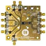
FRONT
BACK
Figure 1. NB3N5573DTGEVB Evaluation Board
© Semiconductor Components Industries, LLC, 2012
February, 2012 − Rev. 1
1
Publication Order Number:
EVBUM2065/D
�NB3N5573DTGEVB
BOARD LAYOUT
SEL1
GND Jack Connector
VDD Jack Connector
VDD ANVIL Connector
SEL0
PIN3
CLK
X1/CLK
CLK
X2
CLK1
CLK1
OE
PIN8
Figure 2. FRONT Board Layout
Figure 3. FRONT Layer Design
http://onsemi.com
2
�NB3N5573DTGEVB
SEL0
GND Jack Connector
VDD Jack Connector
SEL1
CLK
Crystal
PIN3
CLK
X1/CLK
CLK1
X2
CLK1
OE
PIN8
Figure 4. BACK Board Layout
Figure 5. BACK Layer Design
http://onsemi.com
3
�NB3N5573DTGEVB
TEST AND MEASUREMENT SET−UP AND PROCEDURE
Step 1: Equipment
6. Time Transition Convertor: Agilent 14534 250 ps
(or equivalent)
7. Phase noise Analyzer: Agilent E5052B (or
equivalent)
1. Signal Generator: Agilent #33250A or HP8133 (or
equivalent)
2. Tektronix TDS8000 Oscilloscope
3. Power Supply: Agilent #6624A or AG6626A DC
(or equivalent)
4. Digital Voltmeter: Agilent 34410A or 34401 (or
equivalent)
5. Matched Cables (> 20 GHz, SMA connectors):
Storm or Semflex (or equivalent)
Step 2: Lab Set−Up Procedure
1. Test Supply Setup:
Board and Device Power Supply Connections are
shown in Table 1. VDD (Banana Jack or Anvil
Clip test point) and GND (Banana Jack) and may
be connected by.
Table 1. POWER SUPPLY CONNECTIONS
Device
Board
Banana Jack
Anvil Clip
Test Point
VDD
VDD
BJ1
J11
GND
GND
BJ2
J7
SUPPLY (VDD = 3.3 V; GND = 0.0 V’ VEE = 0.0 V)
Comments
DUTGND and SMA GND
CLK1b outputs are directly connected to a LOW impedance
(50 W) module, scope, or probe per Figure 6. Both lines in
an HCSL pair must be terminated.
Single supply operation may be accomplished by
connecting VDD and GND. HCSL CLK, CLKb, CLK1, and
Figure 6. Typical Termination for Output Driver and Device Evaluation
Termination of a signal generator may be accomplished by
placing a 50 W resistor (to GND) at location C42. The
mounted crystal does not need to be removed for Single
Ended input operation.
For Crystal operation use a fundamental Parallel
Resonant crystal (see Datasheet section on “Recommended
Crystal Parameters”) of 25 MHz. The board is supplied with
a thru–hole 25 MHz crystal installed, but alternatively has
the tabs for a surface mount crystal. The Crystal mount is
2. Inputs: (see Appendix 1, Device Pin to Board
Connection Information)
For a Single Ended input to X1/CLK operation, install a
zero ohm jumper resistor at R14. Do not install R16. Do not
drive X2. Use a LVCMOS Clock amplitude signal at 25
MHz which satisfies datasheet VIH and VIL to drive
X1/CLK. Input tr/tf transition edges should be about 250 ps.
Use a TTC (Time transition Convertor) such as Agilent
14534 (250 ps) or equivalent, if needed to slow faster edges.
http://onsemi.com
4
�NB3N5573DTGEVB
LVTTL/LVCMOS input signal levels. Load cap may be
added to fine tune frequency such as 15 pF to GND on both
crystal pins.
Output current reference pin, IREF (Pin9) has a precision
475 W resistor (R5) installed from the output pin to GND to
set the output current.
Inputs OE1 and OE2 may be jumpered to VEE (GND) for
a LOW level (DISABLED) using J15 (OE1) or J12 (OE2).
If floated open (jumper removed), pin will default to a HIGH
level (ENABLED). High Impedance probes must be used to
sense the signal levels.
located on the back (underside) of the board and is
permanently connected to the device inputs by traces.
Crystal load caps should be mounted from each crystal pin
to GND (16 74− 20 pF) to fine tune frequency.
Device frequency is selected by LVTTL/LVCMOS level
inputs SEL0 and SEL1 per datasheet Table 2. Jumpers J12
(SEL0), J13 (SEL1) may be set to either VDD (HI) or GND
(LO), or floated open (HI) to program the output frequency
of operation. Jumpers may be removed to drive SEL0/1b
directly with spec VIH or VIL levels. Note SEL0/1 inputs
will default to VDD when left floating open. High
Impedance probes must be used to sense the
APPENDIX 1: DEVICE PIN TO BOARD CONNECTION INFORMATION (see current Datasheet)
Table 2. DEVICE PINS TO BOARD CONNECTION
Board
Device
Pin
Device Pin
Name
Connection
I/O
Description
1
S0
SEL0
LVTTL/LVCMOS
Input
Frequency select input 0. Internal pullup resistor to VDD. See
datasheet Table 2
2
S1
SEL1
LVTTL/LVCMOS
Input
Frequency select input 1. Internal pullup resistor to VDD. See
datasheet Table 2
3
NC
PIN3
No Connect
No Connect
4
X1/CLK
X1/CLK
Crystal Interface
Oscillator Input from Crystal. Single ended 25 Mhz
LVTTL/LVCMOS Clock Input.
5
X2
X2
Crystal Interface
Oscillator Output to drive Crystal
6
OE
OE
LVTTL/LVCMOS
Input
Output Enable Input pin to control CLKx (tri−states CLKx when
LOW, open pin defaults to HIGH)
7
GND
GND
Ground Supply
DUT and SMA GND Supply. All Supply pins must be
connected for proper operation
8
NC
PIN3
No Connect
No Connect
9
IREF
(−)
10
CLK1b
CLK1b
HCSL Output
HCSL Invert Output
11
CLK1
CLK1
HCSL Output
HCSL True Output
12
VDD
VDD
Positive Supply
Positive Supply pin. All Supply pins must be connected for
proper operation.
13
GND
GND
Ground Supply
DUT and SMA GND Supply. All Supply pins must be
connected for proper operation
14
CLK0b
CLK0b
HCSL Output
HCSL Invert Output
15
CLK0
CLK0
HCSL Output
HCSL True Output
16
GND
GND
Ground Supply
DUT and SMA GND Supply. All Supply pins must be
connected for proper operation
(connects Pin 9 through 475 W to GND)
http://onsemi.com
5
�NB3N5573DTGEVB
APPENDIX 2: SCHEMATIC
Figure 7. Schematic
http://onsemi.com
6
�NB3N5573DTGEVB
APPENDIX 3: BILL OF MATERIALS, LAMINATION STACKUP, AND ASSEMBLY NOTES
Table 3. BILL OF MATERIAL
Item
Qty
Schematic
Value
Size
MFG
P/N
Description
1
2
BJ1−BJ2
ITT POMONA
ELECTRONICS
B−JACK 1/4−32 THREAD
BANANAJACK
2
2
C1,C2
0.1 mF
0402
Panasonic − ECG
ECJ−DEB1A104K
CAP CERM .1UF 10% 10V X5R
3
2
C3,C4
0.01 mF
0402
AVX Corporation
04023C103KAT2A
CAP CERM .01UF 10% 25V X7R
4
1
C9
10 mF
7343
Kemet
T491C106K016AT
CAP TANT 10UF 16V 10% SMD
5
5
J10,J12,J13,J15,J16
2pin
Sullins Electronics
Corp
PEC36SACN
CONN HEADER .100 SINGL STR 36 POS
6
5
J10,J12,J13,J15,J16
Sullins Electronics
Corp
STC02SYAN
CONN JUMPER SHORTING TIN
7
4
R1,R2,R7,R8
33.2
0402
Panasonic − ECG
ERJ−2RKF33R2X
RES 33.2 W 1/16W 1% 0805 SMD
8
4
R3,R4,R9,R10
49.9
0402
YAGEO AMERICA
9C04021A49R8FLHF3
RES 49.9 W 1/16W 1% 0805 SMD
475
0402
Panasonic − ECG
ERJ−2RKF49R9X
RES 475 W 1/16W 1% 0805 SMD
Emerson Network
Power Connectivity
Solutions
142−0701−801
CONN JACK END LAUNCH PCB .187” G
KEYSTONE
ELECTRONICS
5016
PC TEST POINT COMPACT SMT
Ampere
2−330808−8
CONN SOCKET RCPT .013−0.21 30AU
On Semiconductor
NB3N5573DT
16 lead Tssop Dut
9
1
R5
10
11
J1−6,J8,J9,J14,J17,J18
11
1
J11
12
2
Y1 Socket Pins
13
U1
14
4
Standoff
15
4
Screw
16
1
Xtal
ECLIPTEK
ECX−6150−25.000M
XTAL (Do Not Solder)
17
1
SOCKET
M&M
50−000−00809
NOT INSTALLED, Not Provided
SMT
Nylon Standoff
Nylon Screw
Figure 8. Lamination Stack
http://onsemi.com
7
�NB3N5573DTGEVB
http://onsemi.com
8
�onsemi,
, and other names, marks, and brands are registered and/or common law trademarks of Semiconductor Components Industries, LLC dba “onsemi” or its affiliates
and/or subsidiaries in the United States and/or other countries. onsemi owns the rights to a number of patents, trademarks, copyrights, trade secrets, and other intellectual property. A
listing of onsemi’s product/patent coverage may be accessed at www.onsemi.com/site/pdf/Patent−Marking.pdf. onsemi is an Equal Opportunity/Affirmative Action Employer. This
literature is subject to all applicable copyright laws and is not for resale in any manner.
The evaluation board/kit (research and development board/kit) (hereinafter the “board”) is not a finished product and is not available for sale to consumers. The board is only intended
for research, development, demonstration and evaluation purposes and will only be used in laboratory/development areas by persons with an engineering/technical training and familiar
with the risks associated with handling electrical/mechanical components, systems and subsystems. This person assumes full responsibility/liability for proper and safe handling. Any
other use, resale or redistribution for any other purpose is strictly prohibited.
THE BOARD IS PROVIDED BY ONSEMI TO YOU “AS IS” AND WITHOUT ANY REPRESENTATIONS OR WARRANTIES WHATSOEVER. WITHOUT LIMITING THE FOREGOING,
ONSEMI (AND ITS LICENSORS/SUPPLIERS) HEREBY DISCLAIMS ANY AND ALL REPRESENTATIONS AND WARRANTIES IN RELATION TO THE BOARD, ANY
MODIFICATIONS, OR THIS AGREEMENT, WHETHER EXPRESS, IMPLIED, STATUTORY OR OTHERWISE, INCLUDING WITHOUT LIMITATION ANY AND ALL
REPRESENTATIONS AND WARRANTIES OF MERCHANTABILITY, FITNESS FOR A PARTICULAR PURPOSE, TITLE, NON−INFRINGEMENT, AND THOSE ARISING FROM A
COURSE OF DEALING, TRADE USAGE, TRADE CUSTOM OR TRADE PRACTICE.
onsemi reserves the right to make changes without further notice to any board.
You are responsible for determining whether the board will be suitable for your intended use or application or will achieve your intended results. Prior to using or distributing any systems
that have been evaluated, designed or tested using the board, you agree to test and validate your design to confirm the functionality for your application. Any technical, applications or
design information or advice, quality characterization, reliability data or other services provided by onsemi shall not constitute any representation or warranty by onsemi, and no additional
obligations or liabilities shall arise from onsemi having provided such information or services.
onsemi products including the boards are not designed, intended, or authorized for use in life support systems, or any FDA Class 3 medical devices or medical devices with a similar
or equivalent classification in a foreign jurisdiction, or any devices intended for implantation in the human body. You agree to indemnify, defend and hold harmless onsemi, its directors,
officers, employees, representatives, agents, subsidiaries, affiliates, distributors, and assigns, against any and all liabilities, losses, costs, damages, judgments, and expenses, arising
out of any claim, demand, investigation, lawsuit, regulatory action or cause of action arising out of or associated with any unauthorized use, even if such claim alleges that onsemi was
negligent regarding the design or manufacture of any products and/or the board.
This evaluation board/kit does not fall within the scope of the European Union directives regarding electromagnetic compatibility, restricted substances (RoHS), recycling (WEEE), FCC,
CE or UL, and may not meet the technical requirements of these or other related directives.
FCC WARNING – This evaluation board/kit is intended for use for engineering development, demonstration, or evaluation purposes only and is not considered by onsemi to be a finished
end product fit for general consumer use. It may generate, use, or radiate radio frequency energy and has not been tested for compliance with the limits of computing devices pursuant
to part 15 of FCC rules, which are designed to provide reasonable protection against radio frequency interference. Operation of this equipment may cause interference with radio
communications, in which case the user shall be responsible, at its expense, to take whatever measures may be required to correct this interference.
onsemi does not convey any license under its patent rights nor the rights of others.
LIMITATIONS OF LIABILITY: onsemi shall not be liable for any special, consequential, incidental, indirect or punitive damages, including, but not limited to the costs of requalification,
delay, loss of profits or goodwill, arising out of or in connection with the board, even if onsemi is advised of the possibility of such damages. In no event shall onsemi’s aggregate liability
from any obligation arising out of or in connection with the board, under any theory of liability, exceed the purchase price paid for the board, if any.
The board is provided to you subject to the license and other terms per onsemi’s standard terms and conditions of sale. For more information and documentation, please visit
www.onsemi.com.
PUBLICATION ORDERING INFORMATION
LITERATURE FULFILLMENT:
Email Requests to: orderlit@onsemi.com
onsemi Website: www.onsemi.com
◊
TECHNICAL SUPPORT
North American Technical Support:
Voice Mail: 1 800−282−9855 Toll Free USA/Canada
Phone: 011 421 33 790 2910
www.onsemi.com
1
Europe, Middle East and Africa Technical Support:
Phone: 00421 33 790 2910
For additional information, please contact your local Sales Representative
�


 工商网监
湘ICP备2023018690号
工商网监
湘ICP备2023018690号
