ON Semiconductor
Is Now
To learn more about onsemi™, please visit our website at
www.onsemi.com
onsemi and and other names, marks, and brands are registered and/or common law trademarks of Semiconductor Components Industries, LLC dba “onsemi” or its affiliates and/or
subsidiaries in the United States and/or other countries. onsemi owns the rights to a number of patents, trademarks, copyrights, trade secrets, and other intellectual property. A listing of onsemi
product/patent coverage may be accessed at www.onsemi.com/site/pdf/Patent-Marking.pdf. onsemi reserves the right to make changes at any time to any products or information herein, without
notice. The information herein is provided “as-is” and onsemi makes no warranty, representation or guarantee regarding the accuracy of the information, product features, availability, functionality,
or suitability of its products for any particular purpose, nor does onsemi assume any liability arising out of the application or use of any product or circuit, and specifically disclaims any and all
liability, including without limitation special, consequential or incidental damages. Buyer is responsible for its products and applications using onsemi products, including compliance with all laws,
regulations and safety requirements or standards, regardless of any support or applications information provided by onsemi. “Typical” parameters which may be provided in onsemi data sheets and/
or specifications can and do vary in different applications and actual performance may vary over time. All operating parameters, including “Typicals” must be validated for each customer application
by customer’s technical experts. onsemi does not convey any license under any of its intellectual property rights nor the rights of others. onsemi products are not designed, intended, or authorized
for use as a critical component in life support systems or any FDA Class 3 medical devices or medical devices with a same or similar classification in a foreign jurisdiction or any devices intended for
implantation in the human body. Should Buyer purchase or use onsemi products for any such unintended or unauthorized application, Buyer shall indemnify and hold onsemi and its officers, employees,
subsidiaries, affiliates, and distributors harmless against all claims, costs, damages, and expenses, and reasonable attorney fees arising out of, directly or indirectly, any claim of personal injury or death
associated with such unintended or unauthorized use, even if such claim alleges that onsemi was negligent regarding the design or manufacture of the part. onsemi is an Equal Opportunity/Affirmative
Action Employer. This literature is subject to all applicable copyright laws and is not for resale in any manner. Other names and brands may be claimed as the property of others.
�NCS325, NCS2325,
NCS4325
50 mV Offset, 0.25 mV/5C,
35 mA, Zero-Drift
Operational Amplifier
The NCS325, NCS2325 and NCS4325 are CMOS operational
amplifiers providing precision performance. The Zero−Drift
architecture allows for continuous auto−calibration, which provides
very low offset, near−zero drift over time and temperature, and near
flat 1/f noise at only 35 mA (max) quiescent current. These benefits
make these devices ideal for precision DC applications. These op
amps provide rail−to−rail input and output performance and are
optimized for low voltage operation as low as 1.8 V and up to 5.5 V.
The single channel NCS325 is available in the space−saving SOT23−5
package. The dual channel NCS2325 is available in Micro8, SOIC−8,
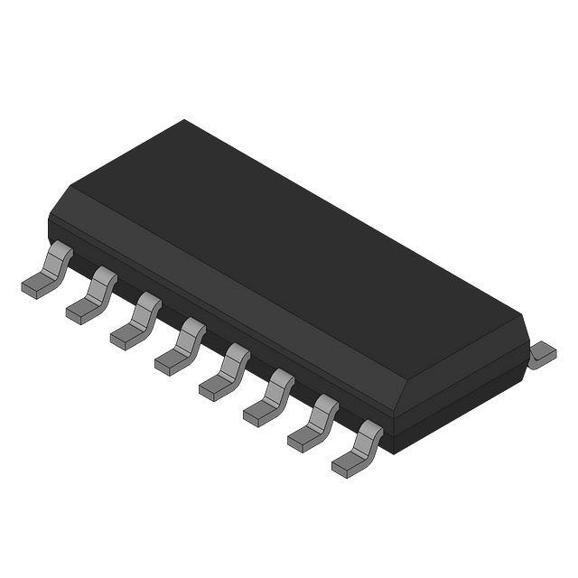
and DFN−8. The quad channel NCS4325 is available in SOIC−14.
Features
•
•
•
•
•
•
•
•
www.onsemi.com
MARKING
DIAGRAMS
1
32A AYWG
G
1
1
DFN−8
MN SUFFIX
CASE 506BW
1
Low Offset Voltage: 14 mV typ, 50 mV max at 25°C for NCS325
Zero Drift: 0.25 mV/°C max
Low Noise: 1 mVpp, 0.1 Hz to 10 Hz
Quiescent Current: 21 mA typ, 35 mA max at 25°C
Supply Voltage: 1.8 V to 5.5 V
Rail−to−Rail Input and Output
Internal EMI Filtering
These Devices are Pb−Free, Halogen Free/BFR Free and are RoHS
Compliant
5
TSOP−5
(SOT23−5)
SN SUFFIX
CASE 483
NCS
2325
ALYWG
G
8
1
SOIC−8
D SUFFIX
CASE 751
N2325
AYWW
G
1
8
MSOP−8
DM SUFFIX
CASE 846A
2325
AYWG
G
1
1
Typical Applications
•
•
•
•
•
•
Battery Powered Instruments
Temperature Measurements
Transducer Applications
Electronic Scales
Medical Instrumentation
Current Sensing
14
1
SOIC−14
D SUFFIX
CASE 751A
NCS4325G
AWLYWW
1
A
= Assembly Location
Y
= Year
WL
= Wafer Lot
W or WW = Work Week
G or G = Pb−Free Package
(Note: Microdot may be in either location)
ORDERING INFORMATION
See detailed ordering and shipping information on page 2 of
this data sheet.
This document contains information on some products that are still under development.
ON Semiconductor reserves the right to change or discontinue these products without
notice.
© Semiconductor Components Industries, LLC, 2017
March, 2017 − Rev. 5
1
Publication Order Number:
NCS325/D
�NCS325, NCS2325, NCS4325
PIN CONNECTIONS
Dual Channel
Single Channel
NCS325
OUT 1
5 VDD
OUT 1 1
IN− 1 2
−
IN+ 1 3
+
8
VDD
7
OUT 2
IN− 1 2
−
− 13 IN− 4
−
6
IN− 2
IN+ 1 3
+
+ 12 IN+ 4
+
5
IN+ 2
VDD
4
IN+ 2
5
+
+ 10
IN+ 3
IN− 2 6
−
−
9
IN− 3
8
OUT 3
OUT 1 1
14 OUT 4
−
2
+
VSS
Quad Channel
NCS4325
NCS2325
IN+ 3
4
IN−
SOT23
VSS 4
DFN−8, SOIC−8, MSOP−8
11
OUT 2 7
VSS
SOIC14
ORDERING INFORMATION
Configuration
Device
Package
Shipping†
Single
NCS325SN2T1G
SOT23−5 / TSOP−5
3000 / Tape & Reel
Dual
NCS2325MNTXG*
(In Development)
DFN8
3000 / Tape & Reel
Quad
NCS2325DR2G
SOIC−8
3000 / Tape & Reel
NCS2325DMR2G
Micro8 / MSOP−8
4000 / Tape & Reel
NCS4325DR2G
SOIC−14
2500 / Tape & Reel
†For information on tape and reel specifications, including part orientation and tape sizes, please refer to our Tape and Reel Packaging
Specifications Brochure, BRD8011/D.
*Contact local sales office for more information
www.onsemi.com
2
�NCS325, NCS2325, NCS4325
ABSOLUTE MAXIMUM RATINGS Over operating free−air temperature, unless otherwise stated.
Parameter
Supply Voltage
Rating
Unit
6
V
INPUT AND OUTPUT PINS
Input Voltage (Note 1)
(VSS) − 0.3 to (VDD) + 0.3
V
Input Current (Note 1)
±10
mA
Output Short Circuit Current (Note 2)
Continuous
TEMPERATURE
Operating Temperature
−40 to +150
°C
Storage Temperature
−65 to +150
°C
Junction Temperature
+150
°C
Human Body Model (HBM)
4000
V
Machine Model (MM)
200
V
100
mA
ESD RATINGS (Note 3)
OTHER RATINGS
Latch−up Current (Note 4)
MSL
Level 1
Stresses exceeding those listed in the Maximum Ratings table may damage the device. If any of these limits are exceeded, device functionality
should not be assumed, damage may occur and reliability may be affected.
1. Input terminals are diode−clamped to the power−supply rails. Input signals that can swing more than 0.3 V beyond the supply rails should
be current limited to 10 mA or less
2. Short−circuit to ground.
3. This device series incorporates ESD protection and is tested by the following methods:
ESD Human Body Model tested per AEC−Q100−002 (JEDEC standard: JESD22−A114)
ESD Machine Model tested per AEC−Q100−003 (JEDEC standard: JESD22−A115)
4. Latch−up Current tested per JEDEC standard: JESD78.
THERMAL INFORMATION
Thermal Metric
Junction to Ambient (Note 5)
Symbol
Package
Value
Unit
qJA
SOT23−5 / TSOP−5
235
°C/W
Micro8 / MSOP−8
298
SOIC−8
250
DFN−8
130
SOIC−14
216
5. As mounted on an 80x80x1.5 mm FR4 PCB with 650 mm2 and 2 oz (0.034 mm) thick copper heat spreader. Following JEDEC JESD/EIA
51.1, 51.2, 51.3 test guidelines
OPERATING CONDITIONS
Parameter
Symbol
Range
Unit
Supply Voltage (VDD − VSS)
VS
1.8 to 5.5
V
Specified Operating Range
TA
−40 to 125
°C
VICMR
VSS−0.1 to VDD+0.1
V
Input Common Mode Voltage Range
Functional operation above the stresses listed in the Recommended Operating Ranges is not implied. Extended exposure to stresses beyond
the Recommended Operating Ranges limits may affect device reliability.
www.onsemi.com
3
�NCS325, NCS2325, NCS4325
ELECTRICAL CHARACTERISTICS: VS = 1.8 V to 5.5 V
At TA = +25°C, RL = 10 kW connected to midsupply, VCM = VOUT = midsupply, unless otherwise noted.
Boldface limits apply over the specified temperature range, TA = −40°C to 125°C, guaranteed by characterization and/or design.
Parameter
Symbol
Conditions
Min
Typ
Max
Unit
mV
INPUT CHARACTERISTICS
Offset Voltage
Offset Voltage Drift vs Temp
VOS
NCS325
VS = +5V
14
50
NCS2325,
NCS4325
VS = +5V
14
75
0.02
0.25
DVOS/DT
TA = −40°C to 125°C
mV/°C
Input Bias Current
IIB
±50
pA
Input Offset Current
IOS
±100
pA
dB
Common Mode Rejection Ratio
CMRR
NCS325
NCS2325,
NCS4325
Input Resistance
RIN
Input Capacitance
CIN
VSS+0.3 < VCM < VDD − 0.3,
VS = 1.8 V
85
108
VSS+0.3 < VCM < VDD − 0.3,
VS = 5.5 V
90
110
VSS+0.3 < VCM < VDD − 0.3,
VS = 5 V
90
110
VSS−0.1 < VCM < VDD + 0.1, VS = 1.8 V
80
VSS−0.1 < VCM < VDD + 0.1, VS = 5.5 V
92
NCS325
NCS2325,
NCS4325
15
GW
Differential
1.8
pF
Common Mode
3.5
pF
Differential
4.1
pF
Common Mode
8.0
pF
OUTPUT CHARACTERISTICS
Output Voltage High
VOH
Output swing within VDD
12
100
mV
Output Voltage Low
VOL
Output swing within VSS
8
100
mV
±5
mA
f = 350 kHz, IO = 0 mA, VS = 1.8 V
1.4
kW
Short Circuit Current
Open Loop Output Impedance
ISC
Zout−OL
f = 350 kHz, IO = 0 mA, VS = 5.5 V
Capacitive Load Drive
2.7
CL
See Figure
NOISE PERFORMANCE
eN
fIN = 1 kHz
100
nV / √Hz
eP−P
fIN = 0.01 Hz to 1 Hz
0.3
mVPP
fIN = 0.1 Hz to 10 Hz
1
mVPP
iN
fIN = 10 Hz
0.3
pA / √Hz
Open Loop Voltage Gain
AVOL
RL = 10 kW, VS = 5.5 V
114
dB
Gain Bandwidth Product
GBWP
kHz
Voltage Noise Density
Voltage Noise
Current Noise Density
DYNAMIC PERFORMANCE
NCS325
CL = 100 pF, RL = 10 kW
350
NCS2325,
NCS4325
CL = 100 pF, RL = 10 kW
270
Phase Margin
fM
CL = 100 pF
60
°
Gain Margin
AM
CL = 100 pF
20
dB
Slew Rate
SR
G = +1, CL = 100 pF, Vs = 1.8 V
0.10
V/ms
G = +1, CL = 100 pF, Vs = 5.5 V
0.16
POWER SUPPLY
Power Supply Rejection Ratio
PSRR
100
TA = −40°C to 125°C
dB
107
95
Turn−on Time
tON
VS = 5 V
100
Quiescent Current
IQ
No load
21
ms
35
mA
Product parametric performance is indicated in the Electrical Characteristics for the listed test conditions, unless otherwise noted. Product
performance may not be indicated by the Electrical Characteristics if operated under different conditions.
www.onsemi.com
4
�NCS325, NCS2325, NCS4325
100
VS = 5 V
VCM = midsupply
TA = 25°C
Sample size = 31
80
60
6
30
0
−30
0
−60
PHASE
−90
−40
−120
−60
−150
−80
0
0
3
6
9
12
15
18
21 24
27
30
10
100
1000
10k
100k
−180
1M
OFFSET VOLTAGE (mV)
FREQUENCY (Hz)
Figure 1. Offset Voltage Distribution
Figure 2. Gain and Phase vs. Frequency
100
100
TA = 25°C
90
VS = 5 V
RL = 10 kW
TA = 25°C
90
80
70
70
PSRR (dB)
80
60
50
40
30
60
50
40
30
20
20
VS = 1.8 V
VS = 5 V
10
0
10
100
10
1000
FREQUENCY (Hz)
0
10
100k
10k
VOH, VS = 5 V
400
VOH, VS = 1.8 V
0
VOL, VS = 1.8 V
−1
−2
VOL, VS = 5 V
1
2
3
4
5
6
10k
100k
1M
300
200
VS = 1.8 V
TA = 25°C
IIB+
IIB−
100
0
−100
−200
−300
−400
−500
−1 −0.8 −0.6 −0.4 −0.2
−3
0
1000
500
TA = 25°C
2
1
100
Figure 4. PSRR vs. Frequency
INPUT BIAS CURRENT (pA)
3
VSS
VDD
FREQUENCY (Hz)
Figure 3. CMRR vs. Frequency
OUTPUT SWING (V)
60
20
−20
4
2
CMRR (dB)
GAIN
40
8
GAIN (dB)
FREQUENCY
10
90
Gain, VS = 1.8 V
Gain, VS = 5.5 V
Phase, VS = 1.8 V
Phase, VS = 5.5 V
PHASE (°C)
12
7
8
9
10
0
0.2
0.4
0.6
0.8
OUTPUT CURRENT (mA)
COMMON MODE VOLTAGE (V)
Figure 5. Output Voltage Swing vs. Output
Current
Figure 6. Input Bias Current vs. Common
Mode Voltage, VS = 1.8 V
www.onsemi.com
5
1
�NCS325, NCS2325, NCS4325
500
500
300
200
100
0
−100
−200
−300
300
200
100
0
−100
−200
−300
−400
−400
−500
−3 −2.5 −2 −1.5 −1
0
0.5
1
1.5
2
2.5
3
−500
−50
3.5
100
125
150
3
TA = 25°C
IIB+
IIB−
VS = 5.0 V
RL = 10 kW
CL = 10 pF
Av = 1 V/V
2
−0.25
−0.5
1
0
−1
−2
−0.75
−0.75
−0.5 −0.25
0
0.25
0.5
DIFFERENTIAL VOLTAGE (V)
0.75
−3
−200
1
−100
0
100
200
300
400
500
TIME (ms)
Figure 9. Input Bias Current vs. Input
Differential Voltage
Figure 10. Large Signal Step Response
0.2
3
VS = 5.0 V
RL = 10 kW
CL = 10 pF
Av = 1 V/V
0.1
0
1
0
−1
−0.1
−2
−100
0
100
200
300
400
Input
Output
2
VOLTAGE (V)
OUTPUT VOLTAGE (V)
70
TEMPERATURE (°C)
0
−0.2
−200
50
Figure 8. Input Bias Current vs. Temperature
0.25
−1
−1
25
0
COMMON MODE VOLTAGE (V)
OUTPUT VOLTAGE (V)
INPUT BIAS CURRENT (pA)
0.5
−25
Figure 7. Input Bias Current vs. Common
Mode Voltage, VS = 5.5 V
1.0
0.75
VS = 5.5 V
IIB+
IIB−
400
INPUT BIAS CURRENT (pA)
INPUT BIAS CURRENT (pA)
400
VS = 5.5 V
TA = 25°C
IIB+
IIB−
−3
−100
500
VS = 5.0 V
RL = 10 kW
CL = 10 pF
Av = −10 V/V
−50
0
50
100
150
TIME (ms)
TIME (ms)
Figure 11. Small Signal Step Response
Figure 12. Positive Over Voltage Recovery
www.onsemi.com
6
200
�NCS325, NCS2325, NCS4325
3
700
Input
Output
SETTING TIME (ms)
VOLTAGE (V)
2
1
0
−1
VS = 5.0 V
RL = 10 kW
CL = 10 pF
Av = −10 V/V
−2
−3
−100
−50
VS = 5.0 V
RL = 10 kW
Output = 4 V Step
600
0
50
100
500
400
300
200
100
150
0
1
200
10
100
TIME (ms)
GAIN (dB)
Figure 13. Negative Over Voltage Recovery
Figure 14. Setting Time vs. Closed Loop Gain
70
VS = 1.8 V
VS = 5.5 V
VOLTAGE (500 nV/div)
OVERSHOOT (%)
60
50
40
30
20
10
RL = 10 kW
Input = 50 mV
0
10
100
1000
LOAD CAPACITANCE (pF)
TIME (1 s/div)
Figure 15. Small Signal Overshoot vs. Load
Capacitance
Figure 16. 0.1 Hz to 10 Hz Noise
1000
CURRENT NOISE (PA/√Hz)
VOLTAGE NOISE (nV/√Hz)
1000
100
10
1
10
VS = 1.8 V
VS = 5.5 V
100
VS = 1.8 V
VS = 5.5 V
100
10
1
0.1
0.01
0.1
1000
1
10
100
1000
FREQUENCY (Hz)
FREQUENCY (Hz)
Figure 17. Voltage Noise Spectral Density vs.
Frequency
Figure 18. Current Noise Spectral Density vs.
Frequency
www.onsemi.com
7
10k
�NCS325, NCS2325, NCS4325
0.2
VS = 5.0 V
VIN = 5 VPP
SR+
0.16
0.12
RL = 10 kW
CL = 100 pF
Av = −10 V/V
VS = 1.8 V
VIN = 1.5 V
SR+
0.1
SR−
0.08
0.06
−40
−20
0
20
40
60
80
100
VS = 5.5 V
25
20
VS = 1.8 V
15
10
5
0
−40
120 140
−20
0
20
40
60
80
100
120 140
TEMPERATURE (°C)
TEMPERATURE (°C)
Figure 19. Slew Rate vs. Temperature
Figure 20. Quiescent Current vs. Temperature
6
VDD Pulse
5
4
3
Output
2
1
0
−1
−20
0
20
40
60
5
4.99
4.98
4.97
4.96
4.95
4.94
4.93
4.92
4.90
4.89
4.88
RL = 10 kW
4.87
TA = 25°C
4.86
80
100
120
TIME (ms)
Figure 21. Turn−on Response
www.onsemi.com
8
OUTPUT VOLTAGE (V)
0.14
QUIESCENT CURRENT (mA)
SR−
VDD VOLTAGE (V)
SLEW RATE (V/ms)
0.18
30
�NCS325, NCS2325, NCS4325
APPLICATIONS INFORMATION
INPUT VOLTAGE
EMI SUSCEPTIBILITY AND INPUT FILTERING
The NCS325, NCS2325 and NCS4325 have rail−to−rail
common mode input voltage range. Diodes between the
inputs and the supply rails keep the input voltage from
exceeding the rails.
Op amps have varying amounts of EMI susceptibility.
Semiconductor junctions can pick up and rectify EMI
signals, creating an EMI−induced voltage offset at the
output, adding another component to the total error. Input
pins are the most sensitive to EMI. The NCS325, NCS2325
and NCS4325 integrate a low−pass filter to decrease its
sensitivity to EMI.
VDD
10 kΩ
IN+
APPLICATION CIRCUITS
+
Low−Side Current Sensing
The goal of low−side current sensing is to detect
over−current conditions or as a method of feedback control.
A sense resistor is placed in series with the load to ground.
Typically, the value of the sense resistor is less than 100 mW
to reduce power loss across the resistor. The op amp
amplifies the voltage drop across the sense resistor with a
gain set by external resistors R1, R2, R3, and R4 (where R1
= R2, R3 = R4). Precision resistors are required for high
accuracy, and the gain is set to utilize the full scale of the
ADC for the highest resolution.
−
IN−
10 kΩ
VSS
Figure 22. Equivalent Input Circuit
R3
VLOAD
VDD
VDD
VDD
Load
R1
Microcontroller
+
ADC
RSENSE
control
−
R2
R4
Figure 23. Low−Side Current Sensing
www.onsemi.com
9
�NCS325, NCS2325, NCS4325
Differential Amplifier for Bridged Circuits
produced is relatively small and needs to be amplified before
going into an ADC. Precision amplifiers are recommended
in these types of applications due to their high gain, low
noise, and low offset voltage.
Sensors to measure strain, pressure, and temperature are
often configured in a Wheatstone bridge circuit as shown in
Figure 24. In the measurement, the voltage change that is
VDD
VDD
−
+
Figure 24. Bridge Circuit Amplification
GENERAL LAYOUT GUIDELINES
the device pins. These techniques will reduce susceptibility
to electromagnetic interference (EMI). Thermoelectric
effects can create an additional temperature dependent
offset voltage at the input pins. To reduce these effects, use
metals with low thermoelectric−coefficients and prevent
temperature gradients from heat sources or cooling fans.
To ensure optimum device performance, it is important to
follow good PCB design practices. Place 0.1 mF decoupling
capacitors as close as possible to the supply pins. Keep traces
short, utilize a ground plane, choose surface−mount
components, and place components as close as possible to
www.onsemi.com
10
�NCS325, NCS2325, NCS4325
PACKAGE DIMENSIONS
TSOP−5
CASE 483−02
ISSUE K
NOTE 5
2X
NOTES:
1. DIMENSIONING AND TOLERANCING PER ASME
Y14.5M, 1994.
2. CONTROLLING DIMENSION: MILLIMETERS.
3. MAXIMUM LEAD THICKNESS INCLUDES LEAD FINISH
THICKNESS. MINIMUM LEAD THICKNESS IS THE
MINIMUM THICKNESS OF BASE MATERIAL.
4. DIMENSIONS A AND B DO NOT INCLUDE MOLD
FLASH, PROTRUSIONS, OR GATE BURRS. MOLD
FLASH, PROTRUSIONS, OR GATE BURRS SHALL NOT
EXCEED 0.15 PER SIDE. DIMENSION A.
5. OPTIONAL CONSTRUCTION: AN ADDITIONAL
TRIMMED LEAD IS ALLOWED IN THIS LOCATION.
TRIMMED LEAD NOT TO EXTEND MORE THAN 0.2
FROM BODY.
D 5X
0.20 C A B
0.10 T
M
2X
0.20 T
B
5
1
4
2
S
3
K
B
DETAIL Z
G
A
A
TOP VIEW
DIM
A
B
C
D
G
H
J
K
M
S
DETAIL Z
J
C
0.05
H
SIDE VIEW
C
SEATING
PLANE
END VIEW
MILLIMETERS
MIN
MAX
3.00 BSC
1.50 BSC
0.90
1.10
0.25
0.50
0.95 BSC
0.01
0.10
0.10
0.26
0.20
0.60
0_
10 _
2.50
3.00
SOLDERING FOOTPRINT*
0.95
0.037
1.9
0.074
2.4
0.094
1.0
0.039
0.7
0.028
SCALE 10:1
mm Ǔ
ǒinches
*For additional information on our Pb−Free strategy and soldering
details, please download the ON Semiconductor Soldering and
Mounting Techniques Reference Manual, SOLDERRM/D.
www.onsemi.com
11
�NCS325, NCS2325, NCS4325
PACKAGE DIMENSIONS
DFN8, 3x3, 0.65P
CASE 506BW−01
ISSUE O
A
B
D
L
NOTES:
1. DIMENSIONING AND TOLERANCING PER
ASME Y14.5M, 1994.
2. CONTROLLING DIMENSION: MILLIMETERS.
3. DIMENSION b APPLIES TO PLATED TERMINAL
AND IS MEASURED BETWEEN 0.15 AND
0.30mm FROM THE TERMINAL TIP.
4. COPLANARITY APPLIES TO THE EXPOSED
PAD AS WELL AS THE TERMINALS.
L
L1
PIN ONE
REFERENCE
2X
0.10 C
ÉÉÉ
ÉÉÉ
ÉÉÉ
0.10 C
2X
DETAIL A
OPTIONAL
CONSTRUCTIONS
E
ÉÉ
ÉÉ
EXPOSED Cu
TOP VIEW
(A3)
DETAIL B
0.05 C
DIM
A
A1
A3
b
D
D2
E
E2
e
K
L
L1
MOLD CMPD
DETAIL B
A
OPTIONAL
CONSTRUCTIONS
MILLIMETERS
MIN
MAX
0.80
1.00
0.00
0.05
0.20 REF
0.25
0.35
3.00 BSC
2.30
2.50
3.00 BSC
1.55
1.75
0.65 BSC
0.20
−−−
0.35
0.45
0.00
0.15
0.05 C
NOTE 4
SIDE VIEW
C
SEATING
PLANE
RECOMMENDED
SOLDERING FOOTPRINT*
D2
DETAIL A
1
8X
A1
ÇÇÇÇÇÇÇÇ
ÇÇÇÇÇÇÇÇ
2.50
4
L
E2
1.75
8X
K
8
5
e/2
e
8X
b
ÇÇÇÇÇÇÇÇ
ÇÇÇÇÇÇÇÇ
1
0.10 C A B
0.05 C
0.65
PITCH
NOTE 3
BOTTOM VIEW
8X
0.62
3.30
8X
0.40
DIMENSIONS: MILLIMETERS
*For additional information on our Pb−Free strategy and soldering
details, please download the ON Semiconductor Soldering and
Mounting Techniques Reference Manual, SOLDERRM/D.
www.onsemi.com
12
�NCS325, NCS2325, NCS4325
PACKAGE DIMENSIONS
SOIC−8 NB
CASE 751−07
ISSUE AK
NOTES:
1. DIMENSIONING AND TOLERANCING PER
ANSI Y14.5M, 1982.
2. CONTROLLING DIMENSION: MILLIMETER.
3. DIMENSION A AND B DO NOT INCLUDE
MOLD PROTRUSION.
4. MAXIMUM MOLD PROTRUSION 0.15 (0.006)
PER SIDE.
5. DIMENSION D DOES NOT INCLUDE DAMBAR
PROTRUSION. ALLOWABLE DAMBAR
PROTRUSION SHALL BE 0.127 (0.005) TOTAL
IN EXCESS OF THE D DIMENSION AT
MAXIMUM MATERIAL CONDITION.
6. 751−01 THRU 751−06 ARE OBSOLETE. NEW
STANDARD IS 751−07.
−X−
A
8
5
S
B
0.25 (0.010)
M
Y
M
1
4
K
−Y−
G
C
N
DIM
A
B
C
D
G
H
J
K
M
N
S
X 45 _
SEATING
PLANE
−Z−
0.10 (0.004)
H
M
D
0.25 (0.010)
M
Z Y
S
X
J
S
SOLDERING FOOTPRINT*
1.52
0.060
7.0
0.275
4.0
0.155
0.6
0.024
1.270
0.050
SCALE 6:1
mm Ǔ
ǒinches
*For additional information on our Pb−Free strategy and soldering
details, please download the ON Semiconductor Soldering and
Mounting Techniques Reference Manual, SOLDERRM/D.
www.onsemi.com
13
MILLIMETERS
MIN
MAX
4.80
5.00
3.80
4.00
1.35
1.75
0.33
0.51
1.27 BSC
0.10
0.25
0.19
0.25
0.40
1.27
0_
8_
0.25
0.50
5.80
6.20
INCHES
MIN
MAX
0.189
0.197
0.150
0.157
0.053
0.069
0.013
0.020
0.050 BSC
0.004
0.010
0.007
0.010
0.016
0.050
0 _
8 _
0.010
0.020
0.228
0.244
�NCS325, NCS2325, NCS4325
PACKAGE DIMENSIONS
Micro8t
CASE 846A−02
ISSUE J
D
HE
PIN 1 ID
NOTES:
1. DIMENSIONING AND TOLERANCING PER ANSI Y14.5M, 1982.
2. CONTROLLING DIMENSION: MILLIMETER.
3. DIMENSION A DOES NOT INCLUDE MOLD FLASH, PROTRUSIONS OR GATE
BURRS. MOLD FLASH, PROTRUSIONS OR GATE BURRS SHALL NOT EXCEED
0.15 (0.006) PER SIDE.
4. DIMENSION B DOES NOT INCLUDE INTERLEAD FLASH OR PROTRUSION.
INTERLEAD FLASH OR PROTRUSION SHALL NOT EXCEED 0.25 (0.010) PER SIDE.
5. 846A-01 OBSOLETE, NEW STANDARD 846A-02.
E
b 8 PL
0.08 (0.003)
−T−
DIM
A
A1
b
c
D
E
e
L
HE
e
M
T B
S
A
S
SEATING
PLANE
A
0.038 (0.0015)
A1
MILLIMETERS
NOM
MAX
−−
1.10
0.08
0.15
0.33
0.40
0.18
0.23
3.00
3.10
3.00
3.10
0.65 BSC
0.40
0.55
0.70
4.75
4.90
5.05
MIN
−−
0.05
0.25
0.13
2.90
2.90
L
c
RECOMMENDED
SOLDERING FOOTPRINT*
8X
8X
0.48
0.80
5.25
0.65
PITCH
DIMENSION: MILLIMETERS
*For additional information on our Pb−Free strategy and soldering
details, please download the ON Semiconductor Soldering and
Mounting Techniques Reference Manual, SOLDERRM/D.
www.onsemi.com
14
INCHES
NOM
−−
0.003
0.013
0.007
0.118
0.118
0.026 BSC
0.021
0.016
0.187
0.193
MIN
−−
0.002
0.010
0.005
0.114
0.114
MAX
0.043
0.006
0.016
0.009
0.122
0.122
0.028
0.199
�NCS325, NCS2325, NCS4325
PACKAGE DIMENSIONS
D
SOIC−14 NB
CASE 751A−03
ISSUE L
A
B
14
NOTES:
1. DIMENSIONING AND TOLERANCING PER
ASME Y14.5M, 1994.
2. CONTROLLING DIMENSION: MILLIMETERS.
3. DIMENSION b DOES NOT INCLUDE DAMBAR
PROTRUSION. ALLOWABLE PROTRUSION
SHALL BE 0.13 TOTAL IN EXCESS OF AT
MAXIMUM MATERIAL CONDITION.
4. DIMENSIONS D AND E DO NOT INCLUDE
MOLD PROTRUSIONS.
5. MAXIMUM MOLD PROTRUSION 0.15 PER
SIDE.
8
A3
E
H
L
1
0.25
M
DETAIL A
7
B
13X
M
b
0.25
M
C A
S
B
S
0.10
e
DETAIL A
h
A
X 45 _
M
A1
C
SEATING
PLANE
DIM
A
A1
A3
b
D
E
e
H
h
L
M
MILLIMETERS
MIN
MAX
1.35
1.75
0.10
0.25
0.19
0.25
0.35
0.49
8.55
8.75
3.80
4.00
1.27 BSC
5.80
6.20
0.25
0.50
0.40
1.25
0_
7_
INCHES
MIN
MAX
0.054 0.068
0.004 0.010
0.008 0.010
0.014 0.019
0.337 0.344
0.150 0.157
0.050 BSC
0.228 0.244
0.010 0.019
0.016 0.049
0_
7_
SOLDERING FOOTPRINT*
6.50
14X
1.18
1
1.27
PITCH
14X
0.58
DIMENSIONS: MILLIMETERS
*For additional information on our Pb−Free strategy and soldering
details, please download the ON Semiconductor Soldering and
Mounting Techniques Reference Manual, SOLDERRM/D.
ON Semiconductor and
are trademarks of Semiconductor Components Industries, LLC dba ON Semiconductor or its subsidiaries in the United States and/or other countries.
ON Semiconductor owns the rights to a number of patents, trademarks, copyrights, trade secrets, and other intellectual property. A listing of ON Semiconductor’s product/patent
coverage may be accessed at www.onsemi.com/site/pdf/Patent−Marking.pdf. ON Semiconductor reserves the right to make changes without further notice to any products herein.
ON Semiconductor makes no warranty, representation or guarantee regarding the suitability of its products for any particular purpose, nor does ON Semiconductor assume any liability
arising out of the application or use of any product or circuit, and specifically disclaims any and all liability, including without limitation special, consequential or incidental damages.
Buyer is responsible for its products and applications using ON Semiconductor products, including compliance with all laws, regulations and safety requirements or standards,
regardless of any support or applications information provided by ON Semiconductor. “Typical” parameters which may be provided in ON Semiconductor data sheets and/or
specifications can and do vary in different applications and actual performance may vary over time. All operating parameters, including “Typicals” must be validated for each customer
application by customer’s technical experts. ON Semiconductor does not convey any license under its patent rights nor the rights of others. ON Semiconductor products are not
designed, intended, or authorized for use as a critical component in life support systems or any FDA Class 3 medical devices or medical devices with a same or similar classification
in a foreign jurisdiction or any devices intended for implantation in the human body. Should Buyer purchase or use ON Semiconductor products for any such unintended or unauthorized
application, Buyer shall indemnify and hold ON Semiconductor and its officers, employees, subsidiaries, affiliates, and distributors harmless against all claims, costs, damages, and
expenses, and reasonable attorney fees arising out of, directly or indirectly, any claim of personal injury or death associated with such unintended or unauthorized use, even if such
claim alleges that ON Semiconductor was negligent regarding the design or manufacture of the part. ON Semiconductor is an Equal Opportunity/Affirmative Action Employer. This
literature is subject to all applicable copyright laws and is not for resale in any manner.
PUBLICATION ORDERING INFORMATION
LITERATURE FULFILLMENT:
Literature Distribution Center for ON Semiconductor
19521 E. 32nd Pkwy, Aurora, Colorado 80011 USA
Phone: 303−675−2175 or 800−344−3860 Toll Free USA/Canada
Fax: 303−675−2176 or 800−344−3867 Toll Free USA/Canada
Email: orderlit@onsemi.com
◊
N. American Technical Support: 800−282−9855 Toll Free
USA/Canada
Europe, Middle East and Africa Technical Support:
Phone: 421 33 790 2910
Japan Customer Focus Center
Phone: 81−3−5817−1050
www.onsemi.com
15
ON Semiconductor Website: www.onsemi.com
Order Literature: http://www.onsemi.com/orderlit
For additional information, please contact your local
Sales Representative
NCS325/D
�


 工商网监
湘ICP备2023018690号
工商网监
湘ICP备2023018690号
